Microwave Packaging for Superconducting Qubits
Benjamin Lienhard, Jochen Braum\"uller, Wayne Woods, Danna Rosenberg,, Greg Calusine, Steven Weber, Antti Veps\"al\"ainen, Kevin O'Brien, Terry P., Orlando, Simon Gustavsson, William D. Oliver

TL;DR
This paper reviews microwave packaging techniques for superconducting qubits, addressing the challenge of controlling their electromagnetic environment to improve circuit performance and scalability in quantum computing.
Contribution
It provides an overview of microwave control methods and discusses engineering solutions for electromagnetic environment management in complex superconducting circuits.
Findings
Enhanced understanding of microwave control in superconducting qubits
Identification of key engineering challenges in electromagnetic environment management
Potential pathways for improving qubit coherence and scalability
Abstract
Over the past two decades, the performance of superconducting quantum circuits has tremendously improved. The progress of superconducting qubits enabled a new industry branch to emerge from global technology enterprises to quantum computing startups. Here, an overview of superconducting quantum circuit microwave control is presented. Furthermore, we discuss one of the persistent engineering challenges in the field, how to control the electromagnetic environment of increasingly complex superconducting circuits such that they are simultaneously protected and efficiently controllable.
Click any figure to enlarge with its caption.
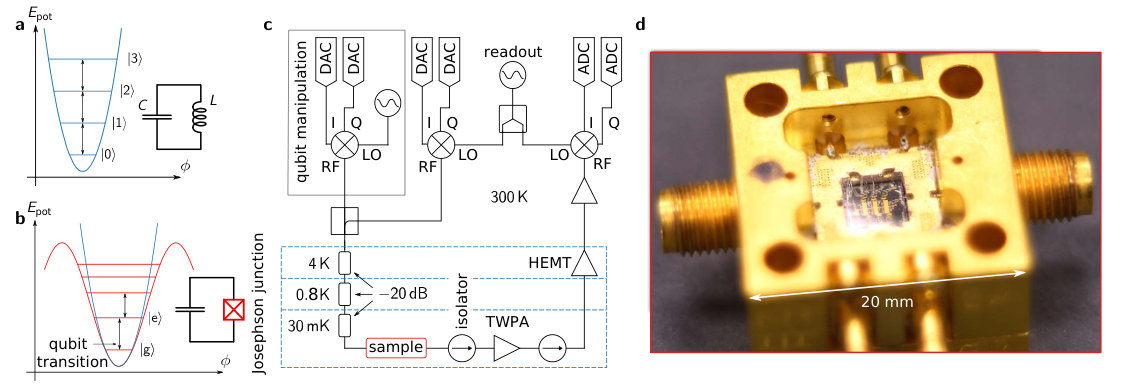 Figure 1
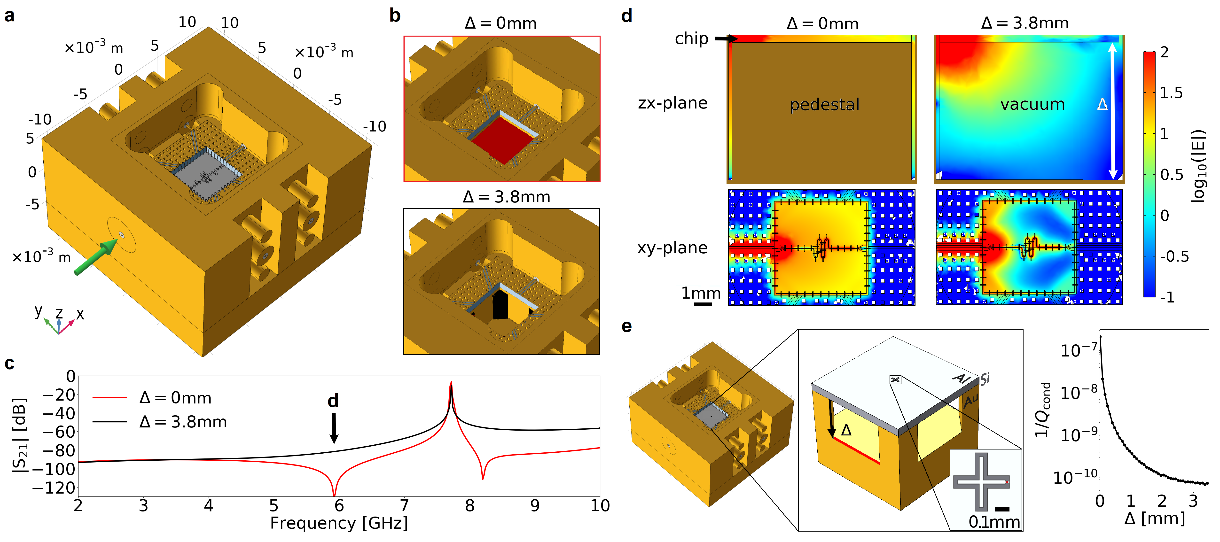 Figure 2
Peer Reviews
No public reviews on file for this paper yet. If you reviewed it on a platform where reviews are public (OpenReview, ICLR, NeurIPS, ICML), you can paste yours below so the community can read it here.
Videos
No videos yet. Explain this paper in a talk, walkthrough, or lecture? Add one.
\IEEEilabelindentA\IEEEilabelindent\IEEEilabelindentA\IEEEelabelindent\IEEEdlabelindent
Microwave Packaging for Superconducting Qubits
Benjamin Lienhard1, Jochen Braumüller2, Wayne Woods3, Danna Rosenberg3, Greg Calusine3,
Steven Weber3, Antti Vepsäläinen2, Kevin O’Brien1,2, Terry P. Orlando1,2, Simon Gustavsson2,
William D. Oliver2,3,4,*,
1 Department of Electrical Engineering & Computer Science, Massachusetts Institute of Technology, USA
2Research Laboratory of Electronics, Massachusetts Institute of Technology, USA
3MIT Lincoln Laboratory, USA
4Department of Physics, Massachusetts Institute of Technology, USA
Abstract
Over the past two decades, the performance of superconducting quantum circuits has tremendously improved. The progress of superconducting qubits enabled a new industry branch to emerge from global technology enterprises to quantum computing startups. Here, an overview of superconducting quantum circuit microwave control is presented. Furthermore, we discuss one of the persistent engineering challenges in the field — how to control the electromagnetic environment of increasingly complex superconducting circuits such that they are simultaneously protected and efficiently controllable.
Keywords:
quantum information processing, microwave components, superconducting circuits, finite element simulations
I Introduction
Universal quantum computation aims to perform specific computational problems such as integer factorization [1] — central to cryptography protocols — or database search [2] in a significantly more efficient way than classical computers. The superconducting qubit modality is a leading candidate today for the realization of such a quantum information processor. Over the last 15 years, the fabrication, design, and control of superconducting qubits have considerably improved, resulting in exponential advancements of coherence properties [3]. The increase in qubit performance has enabled the demonstration of several major milestones in the pursuit of scalable quantum computation. Among others, multi-qubit control and entanglement techniques [4, 5], improved quantum gate fidelities [6], and better readout schemes [7, 8] have enabled the demonstration of small-scale quantum algorithms [9, 10]. However, many engineering challenges need to be overcome to realize the full promise of quantum computation. Here, we present a brief overview of superconducting circuits and present simulations of a sample package with the goal to simultaneously achieve efficient qubit control while suppressing qubit energy decay channels.
II Experimental Methods
II-A The Transmon Qubit
The building blocks of superconducting quantum computing hardware are superconducting qubits, solid-state artificial atoms with level transitions in the microwave regime [11]. The transmon qubit [12] has emerged as one of the most popular qubit designs due to its robust fabrication process, demonstrated operation and readout, and reproducible lifetimes and coherence times in the order of tens of microsenconds [3]. It is closely related to a harmonic -oscillator, which features equidistant energy levels, illustrated in Fig. 1(a). Coherent control requires an isolated pair of energy levels that form a computational qubit basis [13], and this motivates the need for anharmonic oscillators. The necessary anharmonicity is provided by the Josephson junction — a lithographically defined tunnel barrier between two superconducting electrodes — that behaves as a non-linear inductor without any significant dissipation [3]. The schematic transmon circuit is depicted in Fig. 1(b).
By varying the relative strengths of the energies associated with the inductance, capacitance, and tunnel elements in the circuit, various architectures of superconducting qubits can be realized [14], each featuring their own unique noise susceptibility and operation regime [11].
The computational qubit basis is spanned by the ground and excited states and , very much like the two states of a classical bit. However, quantum mechanics enables a qubit to be in any superposition state with probability amplitudes and . Due to quantum correlations (another fundamental concept referred to as entanglement), this leads to quantum parallelism and quantum interference, the two fundamental principles substantiating the power of quantum computations.
II-B Microwave Regime
Despite their macroscopic size, superconducting circuits behave quantum coherently when cooled to milli-Kelvin temperatures. This is mainly due to the absence of conductivity losses in the superconductor when cooled below its critical temperature. Superconducting circuits are fabricated with elementary superconductors such as aluminum, niobium or related compounds such as \chNbN with critical temperatures between and . The circuit operation temperature is small compared to the superconducting gap (50\text{,}\mathrm{G}\mathrm{H}\mathrm{z}) which further suppresses the losses induced by residual unpaired electrons (quasi-particles). The sample operation temperature is $T\sim$10\text{\,}\mathrm{m}\mathrm{K}, achieved by 4\chHe/3\chHe-dilution refrigerators, and corresponds to a frequency of 0.2\text{,}\mathrm{G}\mathrm{H}\mathrm{z}$$ (where and are the Boltzmann and Planck constant, respectively), such that frequency transitions in the regime are only weakly thermally populated and the circuit can approximately be considered to remain in its ground-state in the absence of any controls.
II-C Readout and Control of Superconducting Qubits
Today, superconducting qubit state measurements are most commonly performed using a dispersive readout scheme [7, 8]. The readout device is a resonator that is weakly coupled to the qubit at a detuned frequency. Due to a qubit state dependent “dressing” of the readout resonator, the qubit state can be inferred by spectroscopically probing a dispersive shift of 1\text{,}\mathrm{M}\mathrm{H}\mathrm{z}$$ in its resonance frequency. This scheme enables a quantum non-demolition measurement, where the qubit is mapped onto one of its basis states that corresponds to the measurement outcome [3].
After applying a sequence of quantum gate operations or allowing a free qubit evolution, a measurement process is initiated by populating the readout resonator with a microwave pulse. This is achieved by using an on-chip transmission line coupled to the readout resonator which enables the measurement of microwave reflection or transmission.
Qubit excitation and quantum gates are performed by applying microwave drive pulses at or close to the qubit transition frequency. The qubit undergoes coherent oscillations between its two fundamental basis states, referred to as Rabi oscillations, which can be stopped at any point in time to prepare a desired superposition state. Microwave pulses inducing single-qubit rotations have a typical duration of 20\text{,}\mathrm{ns}$$, and are amplitude modulated by a Gaussian envelope to achieve a localized pulse in Fourier space.
II-D Experimental Setup
A typical microwave measurement setup is schematically depicted in Fig. 1(c). Room temperature electronics feed microwave pulses to the cryostat through coaxial cables with a characteristic impedance matched to .Thesignalspassaseriesofattenuatorswhicharethermallyanchoredtothedifferenttemperaturestages,respectively,inordertosequentiallyreducetheroomtemperatureJohnson-Nyquistnoise,whichformsadecoherencechannelforqubits.\par Measurementpulsesthataretransmittedthroughthesamplearepassedthroughmicrowaveisolatorsbeforetheyreachaquantumlimitedamplifiersuchasatravellingwaveparametricamplifier(TWPA)\cite[cite]{[\@@bibref{}{Macklin307}{}{}]}.TheTWPAamplifiesmicrowavesignalsofindividualphotonsbyabout$$20\text{\,}\mathrm{d}\mathrm{B}$$inabroadbandof∼2\text{\,}\mathrm{G}\mathrm{H}\mathrm{z}$$.Itworksclosetoaregimewhereonlytheminimumamountofnoisedictatedbyquantummechanicsisaddedtotheamplifiedsignal,knownasquantumlimitedamplification.Suchsensitiveamplificationenablesasingle-shotreadoutofasetofqubitsandfacilitatestheimplementationofreal-timequantumfeedback\cite[cite]{[\@@bibref{}{Riste2013a}{}{}]}.Theisolatorspreventleakageofthepumptone,requiredtooperatetheTWPA,backtothesample.Afterpassingalow-noisehighelectronmobilityamplifier(HEMT)attheoutputs,thermalizedto$$4\text{\,}\mathrm{K}$$,thesignalisfurtheramplifiedatroomtemperaturebeforebeingprocessedinroomtemperaturemicrowaveelectronics.\par
II-E Sample Design and Fabrication Techniques
Superconducting quantum circuits are fabricated using commercially available low-loss silicon or sapphire substrates. Primary fabrication processes include thin film evaporation or sputtering of superconducting materials, structured by optical or electron-beam lithography. The dielectric for the Josephson junction tunnel barrier is formed by a controlled in-situ oxidation. The properties and mutual couplings of circuit elements can be individually tailored and fabricated in a reproducible manner due to their macroscopic physical sizes (millimeter-scale) [13].
III Microwave Package Engineering
Superconducting quantum chips are mounted into a sample package which is thermally attached to the cold stage of a dilution refrigerator. It defines the immediate electromagnetic environment of the qubits and connects the quantum circuit to the coaxial control lines.
The primary purpose of a package is to simultaneously shield the quantum circuit from the environment while enabling its efficient control and thermalization. The package can either act as a 3D cavity with an engineered mode spectrum and a high-quality resonance mode used for qubit readout [18], or merely provide an electromagnetic environment with suppressed spurious modes in the frequency spectrum of interest.
The material and geometric design of the sample package need to be chosen such that qubit energy loss channels are suppressed. The qubit can spontaneously dissipate energy to dielectric defects on the surface and interfaces of the sample or by coupling to unwanted package modes. Furthermore, normal metals introduce conductivity loss, which grows with increasing electrical resistance. While conductivity loss in superconducting packages is suppressed, their thermal conductivity is in general strongly reduced, which can result in improper sample thermalization.
Typical package materials are aluminum (: superconducting; : limited; oxide), copper (: high; : high; oxide), or gold-plated copper (: high; : high; limited oxide). The relations between electrical conductivity and thermal conductivity are and . Fig. 1(d) shows the gold-plated copper package used in the simulations presented here. The copper core ensures high thermal conductivity whereas the gold-plating suppresses the formation of a surface oxide layer.
Metallic waveguides for quantum circuit control are imprinted on a dielectric circuit board (interposer [19]) and matched to a characteristic impedance of ∼7.7\text{\,}\mathrm{G}\mathrm{H}\mathrm{z}$$andnotransmissionawayfromresonance.Whenmeasuredinsidethesamplepackage,thetransmissionspectrumoftheresonatorchipisconvolutedwithabroadpackagemodecenteredat∼19\text{\,}\mathrm{G}\mathrm{H}\mathrm{z}$$,mediatinganon-zerobaselinetransmission.\par Fig.~{}\ref{fig:fig2}(b)showsschematicdrawingsoftwosamplepackageversions,onewiththechipsittingonasolidpedestal(red),andonewherethechipissupportedbyfourcornerposts(black)withthepedestaldrilledouttoadistanceofΔ=3.8\text{\,}\mathrm{mm}$$\cite[cite]{[\@@bibref{}{Bronn2018,Wenner2011}{}{}]}.Theresponseoftheon-chipresonatorisvisibleinbothsimulatedtransmissionmagnitudespectra—S_21—(redandblacklinesinFig.~{}\ref{fig:fig2}(c)).Thesimulationofthepackagewithpedestal(red)revealspronouncedpackagemodesintherelevantfrequencyrangewhichprovidesapotentialqubitlosschannel.Theyaresuppressedintheversion(black)withthepedestaldrilledout,indicatinganelectromagneticsampleenvironmentwithoutspuriousmodesinthefrequencyrangeofinterest.Fig.~{}\ref{fig:fig2}(d)showstheelectricfieldmagnitudedistributionatoneoftheboxmodesat$$5.9\text{\,}\mathrm{G}\mathrm{H}\mathrm{z}$$.Forthepackagewithsolidpedestal,theelectricfieldisstronglyenhancedinsideandinthevicinityofthechip.\par Normalmetalnearthesampleformsalosschannelduetofiniteconductivity.TheconductivitylossQ_cond^-1ΔΔ=0\text{\,}\mathrm{m}\mathrm{m}$$,itsaturatesatΔ∼3\text{\,}\mathrm{m}\mathrm{m}$$andissuppressedbyaboutthreeordersofmagnitude.TheextractedconductivitylossforapackagewithsolidpedestalisQ_cond=4.5\text{\times}{10}^{6}\text{\,}$$.SomeofthehighestexperimentallyachievedqubitlifetimesofT_1≈150\text{\,}\mathrm{\SIUnitSymbolMicro}\mathrm{s}$$\cite[cite]{[\@@bibref{}{Oliver2013}{}{}]}correspondtoaqualityfactorofQ≈4.5\text{\times}{10}^{6}\text{\,}$$implyingthatconductivitylosscannotbeneglectedforlong-livedqubits.\par\par\par\par
IV Conclusion
Superconducting circuits are operated in the microwave regime, which enables a high degree of control and provides a rich toolbox of experimental techniques. In return, quantum circuits likewise couple to unwanted microwave modes, making it necessary to provide an engineered electromagnetic environment free of spurious modes in the frequency range of interest, ensured by the sample package. Microwave simulations of the presented sample package indicate that a solid support pedestal below the sample introduces spurious package modes which form a decoherence channel for qubits. In addition, simulations show that the conductivity loss due to a solid pedestal limits the lifetime of long-lived qubits. The conductivity loss can be mitigated by about three orders of magnitude in the studied package by removing the support pedestal.
Acknowledgment
This research is funded by the Office of the Director of National Intelligence (ODNI), Intelligence Advanced Research Projects Activity (IARPA), and by the Assistant Secretary of Defense for Research & Engineering under Air Force Contract No. FA8721-05-C-0002.
The reference list from the paper itself. Each links out to its DOI / PubMed record.
- 1[1] P. W. Shor, “Algorithms for quantum computation: discrete logarithms and factoring,” in Proceedings 35th Annual Symposium on Foundations of Computer Science , Nov 1994, pp. 124–134.
- 2[2] L. K. Grover, “A fast quantum mechanical algorithm for database search,” Proceedings, 28th Annual ACM Symposium on the Theory of Computing , p. 212, may 1996.
- 3[3] W. D. Oliver and P. B. Welander, “Materials in superconducting qubits,” MRS Bulletin , vol. 38, pp. 816–825, oct 2013.
- 4[4] M. Steffen, M. Ansmann, R. C., N. Bialczak, E. L. Katz, R. Mc Dermott, M. Neeley, E. M. Weig, A. N. Cleland, and J. M. Martinis, “Measurement of the entanglement of two superconducting qubits via state tomography,” Science , vol. 313, no. 5792, pp. 1423–1425, 2006.
- 5[5] R. Barends, J. Kelly, A. Megrant, A. Veitia, D. Sank, E. Jeffrey, T. C. White, J. Mutus, A. G. Fowler, B. Campbell, Y. Chen, B. Chiaro, A. Dunsworth, C. Neill, P. O’Malley, P. Roushan, A. Vainsencher, J. Wenner, A. N. Korotkov, A. N. Cleland, and J. M. Martinis, “Superconducting quantum circuits at the surface code threshold for fault tolerance,” Nature , vol. 508, no. 7497, pp. 500–503, 2014.
- 6[6] S. Gustavsson, O. Zwier, J. Bylander, F. Yan, F. Yoshihara, Y. Nakamura, T. P. Orlando, and W. D. Oliver, “Improving quantum gate fidelities by using a qubit to measure microwave pulse distortions,” Phys. Rev. Lett. , vol. 110, no. 4, jan 2013.
- 7[7] A. Blais, R.-S. Huang, A. Wallraff, S. M. Girvin, and R. J. Schoelkopf, “Cavity quantum electrodynamics for superconducting electrical circuits: An architecture for quantum computation,” Phys. Rev. A , vol. 69, no. 6, p. 062320, Jun 2004.
- 8[8] A. Wallraff, D. I. Schuster, A. Blais, L. Frunzio, R.-S. Huang, J. Majer, S. Kumar, S. M. Girvin, and R. J. Schoelkopf, “Strong coupling of a single photon to a superconducting qubit using circuit quantum electrodynamics,” Nature , vol. 431, no. 7005, pp. 162–167, Sep 2004.