Data Conversion in Area-Constrained Applications: the Wireless Network-on-Chip Case
Sergi Abadal, and Eduard Alarc\'on

TL;DR
This paper analyzes the role of data converters, specifically ADCs, in wireless intra-chip communications within Network-on-Chip systems, showing they are feasible despite current limitations.
Contribution
It provides a comprehensive analysis of ADC requirements and performance trends, addressing a previously overlooked aspect of wireless intra-chip communication.
Findings
ADCs are not a major obstacle for wireless intra-chip communication.
Current ADC designs do not fully meet the demands of this application.
Wireless intra-chip communication is viable with existing ADC technology.
Abstract
Network-on-Chip (NoC) is currently the paradigm of choice to interconnect the different components of System-on-Chips (SoCs) or Chip Multiprocessors (CMPs). As the levels of integration continue to grow, however, current NoCs face significant scalability limitations and have prompted research in novel interconnect technologies. Among these, wireless intra-chip communications have been under intense scrutiny due to their low latency broadcast and architectural flexibility. Thus far, the practicality of the idea has been studied from the RF front-end and the network interface perspectives, whereas little to no attention has been placed on another essential component: the data converters. This article aims to fill this gap by providing a comprehensive analysis of the requirements of the scenario, as well as of the current performance and cost trends of Analog-to-Digital Converters (ADCs).…
Click any figure to enlarge with its caption.
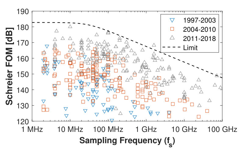 Figure 1
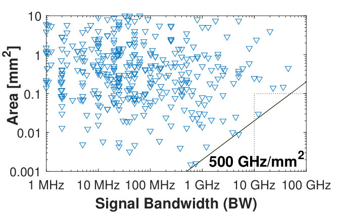 Figure 2
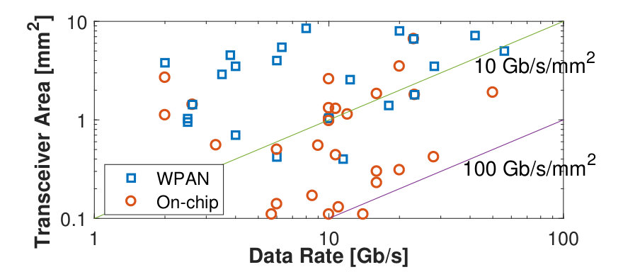 Figure 3
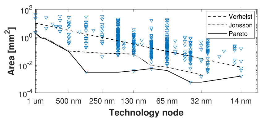 Figure 4
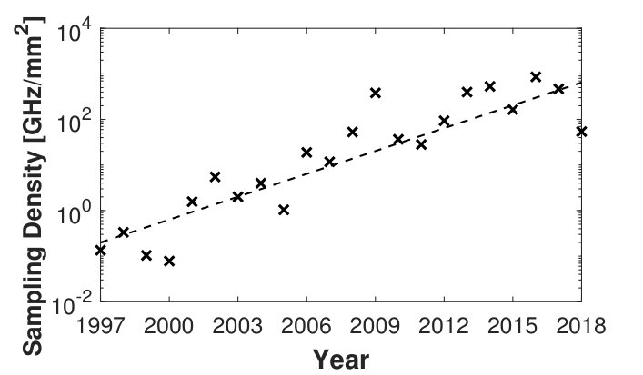 Figure 5
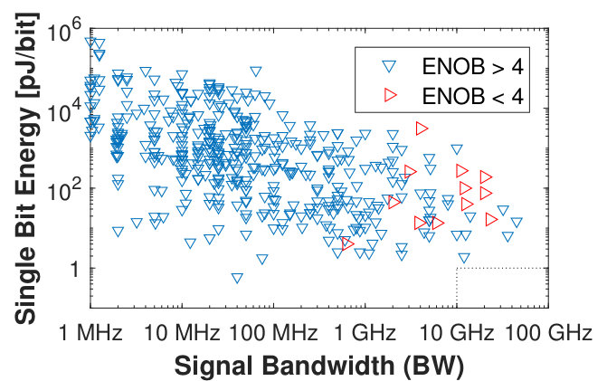 Figure 6
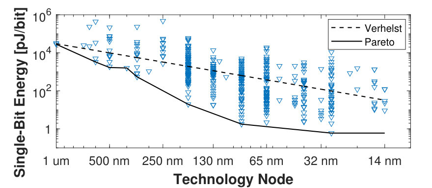 Figure 7
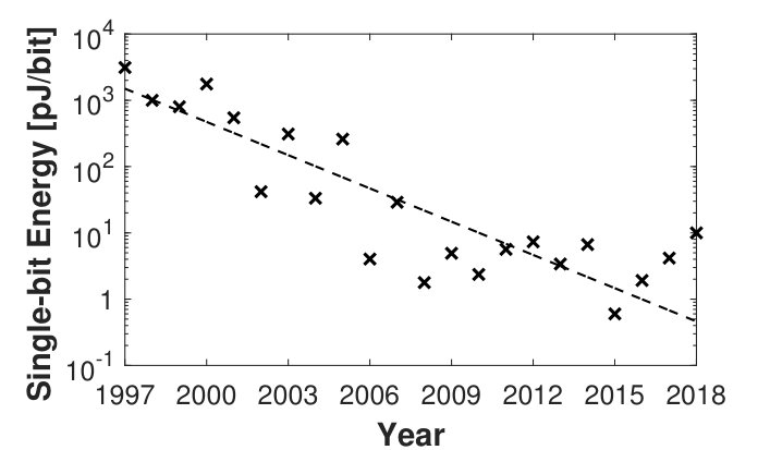 Figure 8
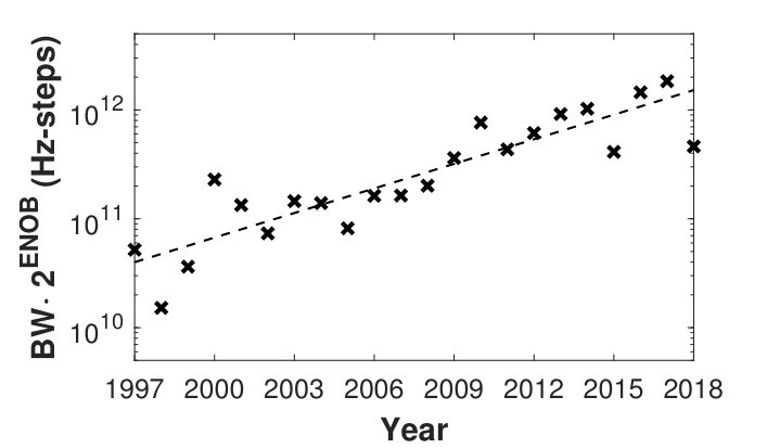 Figure 9
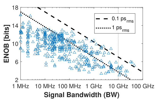 Figure 10
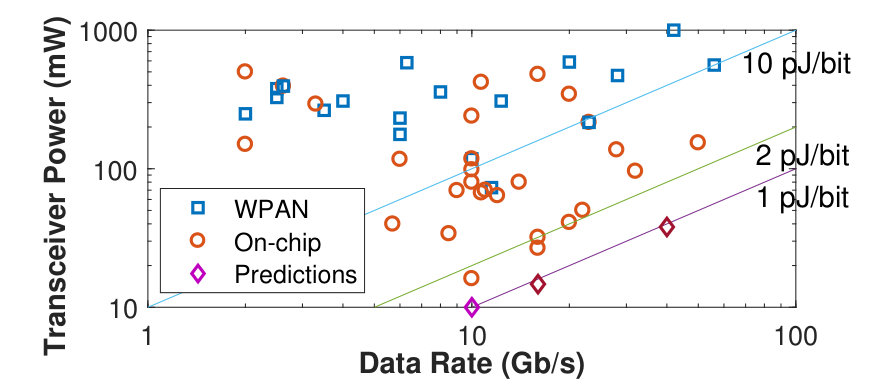 Figure 11
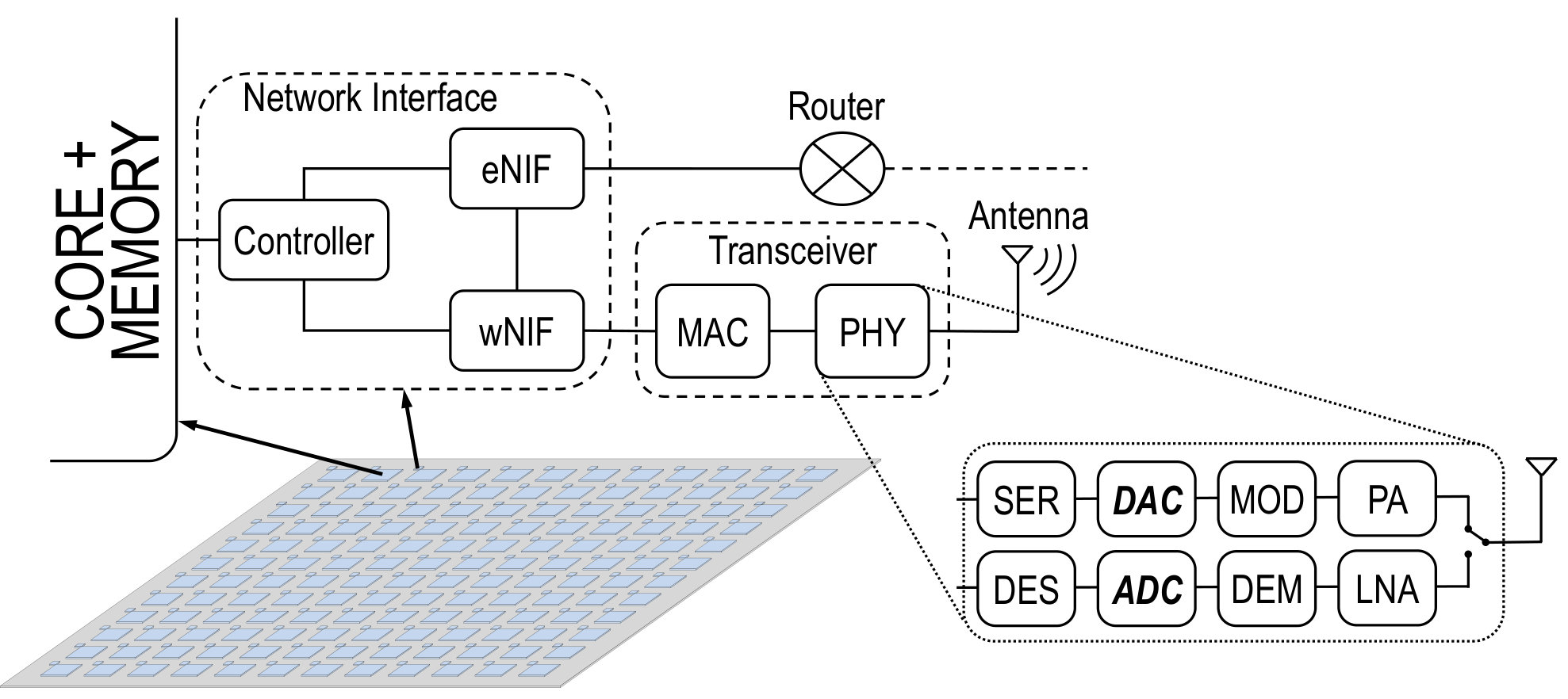 Figure 12
| Metric | Value |
|---|---|
| Transmission Range | 0.1–10 cm |
| Node Density | 10–1000 nodes/cm2 |
| Network Throughput | 10–100 Gb/s |
| Latency | 1–100 ns |
| Bit Error Rate (BER) | 10-15 |
| Transceiver Energy | 1–10 pJ/bit |
| Transceiver Area | 0.01–1 mm2 |
| Metric | Value |
|---|---|
| Signal bandwidth | 10 GHz |
| Nyquist frequency | 20 GHz |
| Oversampling | Null or moderate |
| ENOB | 4 bits |
| Area | 0.1 mm2 |
| Energy | 1 pJ/bit |
Peer Reviews
No public reviews on file for this paper yet. If you reviewed it on a platform where reviews are public (OpenReview, ICLR, NeurIPS, ICML), you can paste yours below so the community can read it here.
Videos
No videos yet. Explain this paper in a talk, walkthrough, or lecture? Add one.
NoC Network-on-Chip WNoC Wireless Network-on-Chip EM Electromagnetic SiO2
Silicon Dioxide AIN Aluminum nitride SiP System-in-Package SDM Software-defined metamaterial RZ Return-to-Zero MAC Medium Access Control THz Terahertz RC Resistive-Capacitive ENOB Effective Number of Bits mm-Wave millimeter-wave OOK On-Off Keying PLL Phase-Locked Loop DAC Digital-to-Analog Converter ADC Analog-to-Digital Converter SAR Successive Approximation Register CDMA Code Division Multiple Access OFDM Orthogonal Frequency Division Multiplexing
Data Conversion in Area-Constrained Applications: the Wireless Network-on-Chip Case
††thanks: This work has been supported in part by the European Commission under grant H2020-FETOPEN-736876 (VISORSURF) and the Spanish MINECO under contract TEC2017-90034-C2-1-R (ALLIANCE).
Sergi Abadal
*Computer Architecture Department
Universitat Politècnica de Catalunya
*Barcelona, Spain
Eduard Alarcón
*Electrical Engineering Department
Universitat Politècnica de Catalunya
*Barcelona, Spain
Abstract
Network-on-Chip (NoC) is currently the paradigm of choice to interconnect the different components of System-on-Chips (SoCs) or Chip Multiprocessors (CMPs). As the levels of integration continue to grow, however, current NoCs face significant scalability limitations and have prompted research in novel interconnect technologies. Among these, wireless intra-chip communications have been under intense scrutiny due to their low latency broadcast and architectural flexibility. Thus far, the practicality of the idea has been studied from the RF front-end and the network interface perspectives, whereas little to no attention has been placed on another essential component: the data converters. This article aims to fill this gap by providing a comprehensive analysis of the requirements of the scenario, as well as of the current performance and cost trends of Analog-to-Digital Converters. Based on Murmann's data, we demonstrate that ADCs will not be a roadblock for the realization of wireless intra-chip communications although current designs do not meet their demands fully.
Index Terms:
Wireless Network-on-Chip; High-Speed Data Conversion; DAC; ADC
I Introduction
Network-on-Chip (NoC) has become the paradigm of choice to interconnect cores and memory within a chip. However, recent years have seen a significant increase in the core density and, within this context, it becomes increasingly difficult to meet the on-chip communication requirements with conventional NoCs alone [1]. Their limited scalability is gradually turning communication, not computation, into the performance bottleneck in parallel processing. New solutions are thus required to avoid slowing down progress in the manycore era [2].
Advances in integrated millimeter-wave (mm-Wave) antennas [3, 4] and transceivers [5, 6] have led to the proposal of Wireless Network-on-Chip (WNoC) as a potential alternative to conventional NoC fabrics [7]. In a WNoC, a set of cores is augmented with transceivers and antennas capable of modulating and radiating the information. RF signals propagate through the computing package and can be demodulated by all tuned-in receivers. The main advantage of this approach is that distant cores can communicate with low latency as propagation occurs nearly at the speed of light. In fact, communication is naturally broadcast. Further, the wireless approach provides an architectural flexibility very hard to achieve with wired alternatives.
Due to its potential, WNoCs have been investigated extensively from different standpoints [7, 8, 9]. At the circuit level, most efforts have focused on the design of the analog front end [6] or aspects around it, e.g., power gating [10]. In contrast, and despite being a critical function in any wireless system, data conversion has been generally overlooked or taken for granted. However, at speeds over 10 Gb/s and given the evident resource limitations of nowadays chips, such an assumption is far from trivial even for simple modulations. Advanced options such as Code Division Multiple Access (CDMA) [11] or Orthogonal Frequency Division Multiplexing (OFDM) [12] may be simply out of question in this scenario.
In this paper, we aim to provide a feasibility analysis of data conversion in the WNoC scenario. We first estimate the data conversion demands of the WNoC paradigm by the order of magnitude. Then, we use historical figures from actual converter implementations [13, 14] to update existing performance and energy efficiency predictions, as illustrated in Figure 1. Area scaling trends, which have been given much less attention in the literature [15, 16], are also studied in depth here in light of the chip real state restrictions of the on-chip scenario. With this, we are able to assess whether data conversion will be a roadblock in the realization of the WNoC or not, and under which conditions.
In a broader sense, the analysis would be applicable to other wireless applications with evident resource constraints such as Wireless Nanosensor Networks (WNSNs) [17] or Software-Defined Metamaterials (SDMs) [18]. In any case, and to the best of the author's knowledge, this is the first gap analysis relative to data conversion in emerging area-constrained applications.
The remainder of this paper is organized as follows. Section II reviews the main wireless channel and physical considerations of the WNoC case, to then derive a rough quantification of the requirements for data converters. Section III discusses how close are current designs from being able to accommodate the predicted WNoC requirements, whereas Section IV extrapolates future behavior from on-going performance and cost trends. Finally, Section V concludes the paper.
II Wireless Network-on-Chip: System Considerations
Figure 2 exemplifies the WNoC paradigm, basically comprising a co-integration of antennas and transceivers with cores in complement of the wired Network-on-Chip (NoC). As an asymptotic case, let us assume that wireless communication capabilities are given at the core level. However, note that other works may assume a reduced number of wireless interfaces through clustering or co-integration with the routers [19]. In either case, WNoCs are only considered in large manycores (i.e., tens or hundreds of cores), where communications can become a performance bottleneck.
In this context, the network interface performs address translation, load balancing, and admission control; whereas the Medium Access Control (MAC) module performs the usual actions to ensure that all nodes can access the shared medium without collisions. At the physical layer, four functions common to any wireless system interfaced to a digital architecture are performed: serialization, data conversion, modulation, and power amplification. Next, we describe several design considerations that have a potential impact on the data conversion process.
General Considerations. Table I provides a rough quantification of the communication requirements in a WNoC, substantiated by the following. As mentioned above, communications are crucial in manycores as they can become the system bottleneck if not served well. For this reason, latency and throughput objectives are set to very ambitious levels for wireless communications, with latencies in the nanosecond scale and throughputs in the order of tens of Gb/s, to compete with chip-wide wired NoC options. Additionally, the error rates are generally assumed to be similar to that of Resistive-Capacitive (RC) wires.
Besides high performance, WNoCs must also seek cost efficiency both in terms of area and power. Area constraints are evident given that the dimensions of a chip, typically 2020 mm2, do not scale up with the number of cores [20]. Multiprocessor systems are also energy-aware, if not energy-limited, because the available total power does not scale with the number of cores either, mainly due to heat dissipation issues [20]. Therefore, manycore systems account for a strict power budget so that the Thermal Design Point (TDP), varying from tens to a few hundreds of Watts, is always respected.
Assuming a 100-core processor in a 450 mm2 chip with the TDP of a Xeon Phi (210 W), we will thus have that each core can only take 4.5 mm2 and at most 2.1 W of sustained power including the processor, memory, and communication sub-systems. Optimistically assuming the same budget for the three sub-systems, the NoC (including the wireless part, if any) should not exceed 1.5 mm2 and not take more of 700 mW per core. Assuming again an equitable distribution of resources and neglecting network interface and MAC overheads, we would estimate the WNoC to have a budget of around 0.75 mm2 and 350 mW per core (3.5 pJ/bit at 100 Gb/s or around 35 pJ/bit at 10 Gb/s). Let this estimation serve as reasonable limits for the cost of a WNoC, noting that they would be increased or reduced depending on the actual distribution of resources and the number of cores.
Transceiver cost. Most of the overhead of the WNoC is expected to come from the analog front-end at the physical layer. To estimate it, one can take base on existing designs optimized for this scenario [6], which report performance and costs compliant with the above estimations. Another route is to include these designs in a wider exploration of the state of the art, which may allow us to also obtain trends. In this respect, Figure 3 shows the area and power of a set of transceiver designs for multi-Gb/s short-range wireless communications reported in the period of 2010–2018. Note that the antenna is not included in such analysis.
The main outcome of Figure 3 is the confirmation of that (1) the throughput objectives are well achievable, and (2) most of the area and power budgets for WNoC will be taken by the transceiver and the antenna. Therefore, there is not much room to spare for the data converters and the serializer circuits. For the purpose of this article, let us assume that at most 10% of the whole transceiver area and power will be devoted to data conversion. In other words:
- •
Conversion circuits should occupy less than 0.1 mm2.
- •
Conversion should consume less than 1 pJ/bit.
Modulation. WNoC uses mm-Wave frequencies and points to the Terahertz (THz) band so that the antennas become commensurate with the cores in manycore settings. This pushes the requirements of the components of the transceiver limiting, together with the area and power constraints themselves, the complexity of the underlying modulation. As a result, most works in WNoC assume simple modulation schemes such as On-Off Keying (OOK) and non-coherent detection [21]. Modulations requiring detection or phase or precise synchronization are avoided whenever possible, as Phase-Locked Loop (PLL) circuits are extremely power-hungry. Simplicity, together with the stringent error rate requirements, are also the main reasons of advocating for modulations with low spectral efficiency. Equalization and other advanced signal processing methods are also out of question for the same reasons.
Simplicity in the modulation has several consequences at the data conversion stage, such as:
- •
Depending on the transmitting circuit topology and modulation, Digital-to-Analog Converters may be completely bypassed.
- •
At the ADC, the sampling frequency will be pushed to speeds over tens of GS/s to comply with the throughput requirements.
- •
At the ADC, the required Effective Number of Bits (ENOB) will be quite low as very few bits per sample are required (potentially down to one).
Wireless Channel. Unlike in other wireless scenarios, communications in WNoC take place in an enclosed and static environment [22]. This has different implications on the design of the physical and MAC layers of the protocol stack. For instance, the enclosed nature of the chip package leads to low path loss exponents [23], but is also expected to lead to long delay spreads. Fortunately, the static environment could allow the development of opportunistic solutions at the receiver, perhaps employing Return-to-Zero (RZ) techniques or adaptive decision circuits. Being static, the chip environment would also allow the detection of collisions through unconventional approaches, such as the comparison of the received RF power with the source address of the packet [24].
The main consequences of the above considerations on the data conversion are the following:
- •
Moderate oversampling may be needed to meet the data rate requirements.
- •
Additional bits per sample may be also used to improve performance.
III Gap Analysis
Table II shows a summary of the ADC requirements in WNoC derived from the order-of-magnitude estimations made in Section II. Here, we discuss current figures of state-of-the-art ADCs to assess whether current designs can meet expected WNoC requirements. To this end, we take base on the widely recognized dataset by Murmann, which is considered an exhaustive and representative survey of ADC designs for the last 20 years [25]. At the time of this writing, this dataset contains more than 500 entries coming from the flagship conferences in Solid-State Circuits (IEEE ISSCC) and Very Large Scale Integration Circuits (IEEE VLSIC). We analyze performance, area, and power consumption.
III-A Performance
To evaluate performance, we focus on the signal bandwidth . Since we assume the use of low order modulations, the data rate (in Gb/s) tends to be equal to (in GHz). The ADC needs to provide sampling at the Nyquist rate at least, or at higher sampling rates for a given oversampling ratio , so that
[TABLE]
Figure 4(a) shows a reinterpretation of the conventional aperture graph, plotting ENOB as a function of the signal bandwidth in our case. It is observed that recent ADCs achieve the required 10 GHz, with the greatest bandwidth being 45 GHz with an impressive Nyquist rate of 90 GS/s [26]. However, this and subsequent designs at 72 and 64 GS/s could not provide valid ENOB measurements at such high bandwidths. Duan et al., instead, are capable of proving 23 GHz of signal bandwidth at Nyquist rate of 46 GS/s with an ENOB of around 4 bits [27].
Additionally, Figure 4(a) illustrates the upper performance bounds of ADCs limited by jitter, which helps quantify the maximum admissible noise level at the clocks. Although several designs already pushed the 0.1 ps limit and femtosecond values are possible with photonic alternatives [28], ADCs for WNoC do not need to move past those barriers thanks to their relatively low ENOB requirement.
III-B Energy Consumption
To evaluate energy consumption, let us assume that all bits coming from the ADC are used for the decoding of symbols modulated at 1 b/s/Hz, as per simplicity requirements at the transceiver. In line with the limited bit depth requirements of WNoC, extra ADC bits would be wasted. Taking this into consideration, we define the single-bit energy as
[TABLE]
where is the power consumption at the ADC. The results are expressed in pJ/bit and aim to convey a measure of the energy consumed by the ADC per each modulated bit, analogous to the bit energy at the transceiver.
Figure 4(b) represents the single-bit energy as a function of the signal bandwidth, distinguishing between low and high ENOB designs. A first observation is that none of the reported ADCs is capable of providing the required efficiency. The closest is the design by Xu et al. again, which consumes 23 mW providing 12 GHz of bandwidth and therefore should be at least halved to reach the WNoC requirements. Another striking result is that low ENOB designs, which would be theoretically less power-hungry than the high ENOB ones, are very sparse and do not present better efficiencies overall. However, we speculate that the low ENOB requirements of the scenario could help minimize the power consumption.
III-C Area Overhead
In data converters, area has been always accounted for, but never seen as a primary concern. In chip-scale communications, however, the chip real estate is limited and ADCs should minimize their active area. However, high speeds require either complex circuits or a considerable number stages in time-interleaved architectures, complicating the task of delivering compact yet fast designs.
As observed in Figure 4(c), only a 2017 design by Xu et al. [29] is capable of barely meeting the requirements of the WNoC scenario thanks to its 0.03 mm2 and 12 GHz of bandwidth (Nyquist rate of 24 GS/s) implemented in 28-nm CMOS. A few proposals, including this one, have an ADC area so that they achieve a sampling density
[TABLE]
of around 500 GHz/mm2. This is about one order of magnitude larger than the bandwidth density of the transceiver (Fig. 3). It is expected that as high-speed ADCs mature and technologies below 32-nm CMOS become widespread, new designs will be able to surpass this barrier and enter the desired target area, as we will see next.
IV Discussion: Future Trends
The results obtained in Section III demonstrate that latest ADCs are at the verge to achieving the performance and efficiency demanded by WNoC, but also that improvements are needed especially in terms of energy consumption. Here, we provide an analysis of the on-going scaling trends with the aim to anticipate the feasibility of the data conversion in our target scenario.
IV-A Temporal Evolution and Limits
Performance. Murmann has formulated several scaling trends in several publications by analyzing the designs that push the envelope. For instance, in 2015 he stated that the speed–resolution product () doubles every four years [14] and, as observed in Figure 5(a), the trend continues nowadays. Given that the maximum achievable ENOB does not vary much among generations, it is reasonable to affirm that ADCs with higher speeds will continue to appear in the following years and that 100-Gb/s systems could be a reality at some point.
Energy Consumption. Another trend assessed by Murmann in [14] relates to the Schreier's figure of merit, which expresses the energy efficiency of an ADC through
[TABLE]
where is the signal-to-noise-distortion ratio. As observed in Figure 1, designs reach a practical limit which has been extended over the years vertically at low frequencies and to the right at high frequencies. In the latter case, which better applies to our scenario, the trend is that the sampling frequency for which we can achieve a given level of doubles every 1.8 years.
The evolution of the Schreier's FOM provides the intuition that the energy consumption can be reduced in a similar pace, as we show in Figure 5(c), which plots the best reported each year. Murmann's tendency, also drawn, provides a good approximation of what we can expect in future years.
Here, it is worth noting that our discussion is far from the fundamental limit on energy consumption. Such limit is given by the minimum energy required to drive a sampling capacitor using an ideal (Class-B) amplifier [14]
[TABLE]
where is the Boltzmann constant and is the temperature, and is the signal-to-noise ratio. For the low ENOB requirements that we have, this formulation sets the fundamental limit more than 3 orders of magnitude below our most stringent target of 0.1 pJ/bit.
Area. Although no specific area trends have been formulated in the related work, we speculate that the tendency above could also be applied here. To confirm this, we evaluate the sampling density with Equation (3) and plot the best value per year. The results shown in Figure 5(b) suggests that, indeed, the sampling density also may be doubling every 1.8 years.
IV-B Impact of Technology Downscaling
The scaling trends demonstrated are product of the downscaling of technology, as well as of circuit optimizations that are realized as new technologies mature. The impact on energy and area is in principle clear, as transistors become smaller, faster, and can be driven with lower voltages. However, side-effects such as leakage or parasitics that appear when pushing the technology to the limit may dilute those advantages. In any case, some works have inspected the impact of technology downscaling. Here, we update the analysis of [15, 16] with the 2018 version of Murmann's data.
In terms of energy, the analysis from [16] predicted an average improvement of where is the technology feature size. Figure 6(a) confirms that thus tendency is a good approximation of average behavior. Note, however, that some ADC architectures benefit more from technology scaling. For instance, Successive Approximation Register (SAR) ADCs obtain up to as stated in [16] and recently confirmed in [30], turning them into a great choice for high-speed efficient conversion. The work by Xu et al., arguably the best candidate for WNoC, is actually a SAR ADC.
In terms of area, the works by Jonsson [15] and Verhelst [16] concluded that average behavior scales as and , respectively. They are both represented in Figure 6(b), and at first sight the answer by Verhelst seems to better fit the data in average.
The Pareto optimality analysis seems to imply, that by reaching sub-20nm technologies, we can expect a slight saturation of the area and energy benefits when downscaling. This may be due to tunneling at the transistors and other undesired effects, but also needs confirmation as technology matures and new optimization techniques are worked out.
V Conclusion and Future Perspectives
This paper has provided an estimation of the ADC requirements in the WNoC scenario. Taking base on low-order modulations, high signal bandwidths (well over 10 GHz) and stringent area and energy limitations (below 1 pJ/bit and 0.1 mm2) are expected. Current ADC designs barely meet these demands, but on-going scaling trends suggest that data conversion will not become a bottleneck in WNoCs. We estimate that high-speed ADCs at 0.1 pJ/bit and 0.01 mm2, or even below, can be a reality in 5–10 years unless WNoC-specific designs are attempted. In such case, one-bit quantization and undersampling techniques could be explored with the aim of softening the technical requirements of ADCs and paving the way towards the realization of the WNoC paradigm.
Acknowledgments
The authors thank Alejandro López-Lao for his technical support and discussions during the development of this work.
The reference list from the paper itself. Each links out to its DOI / PubMed record.
- 1[1] D. Bertozzi, G. Dimitrakopoulos, J. Flich, and S. Sonntag, ``The fast evolving landscape of on-chip communication,'' Design Automation for Embedded Systems , vol. 19, no. 1, pp. 59–76, 2015.
- 2[2] J. Kim, K. Choi, and G. Loh, ``Exploiting new interconnect technologies in on-chip communication,'' IEEE Journal on Emerging and Selected Topics in Circuits and Systems , vol. 2, no. 2, pp. 124–136, 2012.
- 3[3] O. Markish, B. Sheinman, O. Katz, D. Corcos, and D. Elad, ``On-chip mm Wave Antennas and Transceivers,'' in Proceedings of the No CS '15 , 2015, p. Art. 11.
- 4[4] H. M. Cheema and A. Shamim, ``The last barrier: On-chip antennas,'' IEEE Microwave Magazine , vol. 14, no. 1, pp. 79–91, 2013.
- 5[5] S. Laha, S. Kaya, D. W. Matolak, W. Rayess, D. Di Tomaso, and A. Kodi, ``A New Frontier in Ultralow Power Wireless Links: Network-on-Chip and Chip-to-Chip Interconnects,'' IEEE Transactions on Computer-Aided Design of Integrated Circuits and Systems , vol. 34, no. 2, pp. 186–198, 2015.
- 6[6] S. Subramaniam, T. Shinde, P. Deshmukh, S. Shamim, M. Indovina, and A. Ganguly, ``A 0.36p J/bit, 17Gbps OOK Receiver in 45-nm CMOS for Inter and Intra-Chip Wireless Interconnects,'' in Proceedings of the SOCC '17 , 2017.
- 7[7] D. Matolak, A. Kodi, S. Kaya, D. Di Tomaso, S. Laha, and W. Rayess, ``Wireless networks-on-chips: architecture, wireless channel, and devices,'' IEEE Wireless Communications , vol. 19, no. 5, 2012.
- 8[8] R. G. Kim, W. Choi, G. Liu, E. Mhandesi, P. P. Pande, D. Marculescu, and R. Marculescu, ``Wireless No C for VFI-Enabled Multicore Chip Design: Performance Evaluation and Design Trade-offs,'' IEEE Transactions on Computers , vol. 65, no. 4, pp. 1323–36, 2015.