Wurtzite Phonons and the Mobility of a GaN/AlN 2D Hole Gas
Samuel James Bader, Reet Chaudhuri, Martin Schubert, Han Wui Then,, Huili Grace Xing, Debdeep Jena

TL;DR
This paper analyzes phonon spectra in GaN/AlN heterostructures and models their impact on 2D hole gas mobility, proposing strain engineering to improve p-channel device performance in wide-bandgap electronics.
Contribution
It provides a detailed phonon spectrum analysis and models phonon-hole interactions, introducing strain engineering as a method to enhance 2D hole mobility in GaN/AlN heterostructures.
Findings
Identified key phonon modes affecting hole mobility.
Quantified temperature dependence of mobility.
Suggested strain engineering to improve device performance.
Abstract
To make complementary GaN electronics more than a pipe dream, it is essential to understand the low mobility of 2D hole gases in III-Nitride heterostructures. This work derives both the acoustic and optical phonon spectra present in one of the most prominent p-channel heterostructures (the all-binary GaN/AlN stack) and computes the interactions of these spectra with the 2D hole gas, capturing the temperature dependence of its intrinsic mobility. Finally, the effects of strain on the electronic structure of the confined 2D hole gas are examined and a means is proposed to engineer the strain to improve the 2D hole mobility for enhanced p-channel device performance, with the goal of enabling wide-bandgap CMOS.
Click any figure to enlarge with its caption.
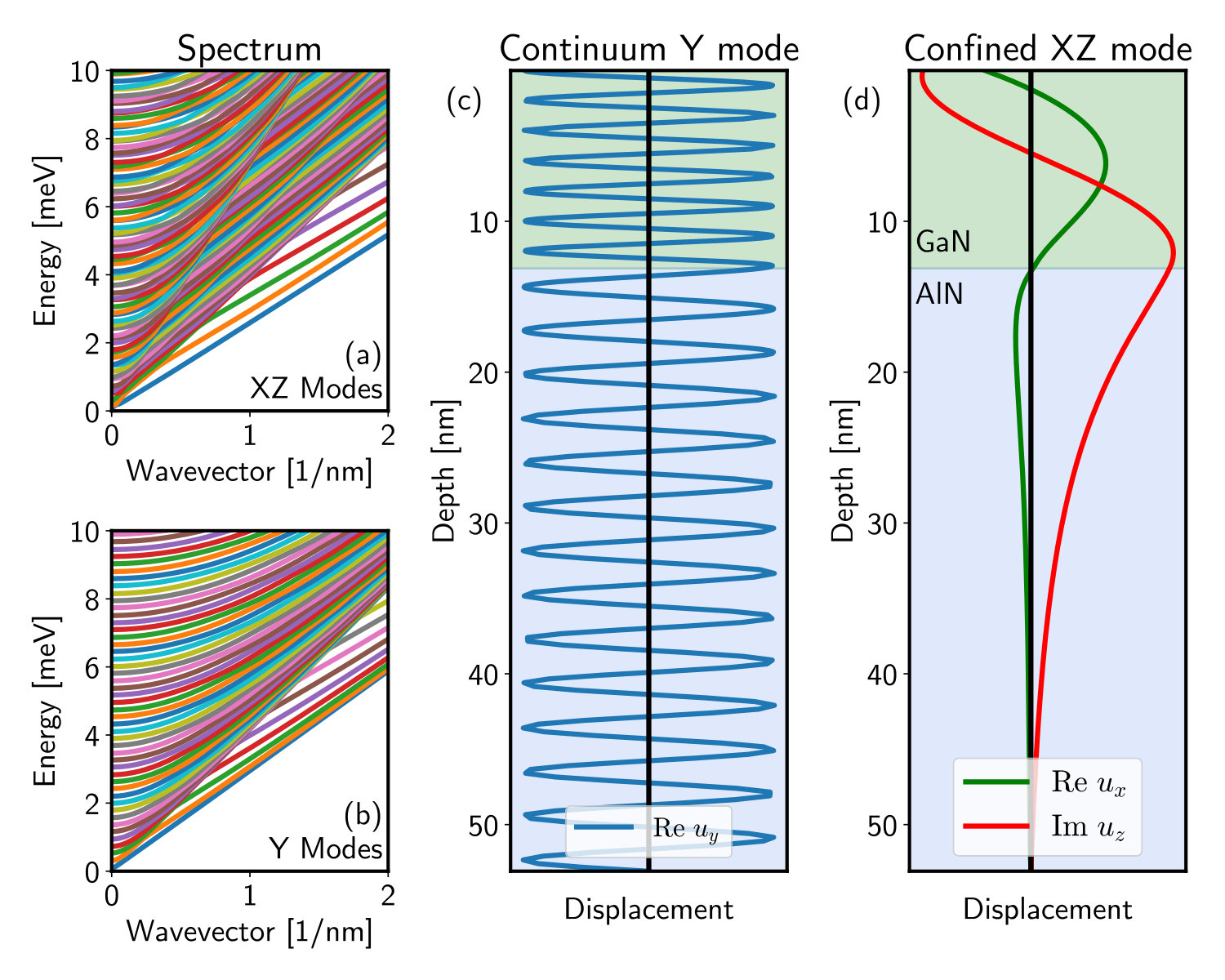 Figure 1
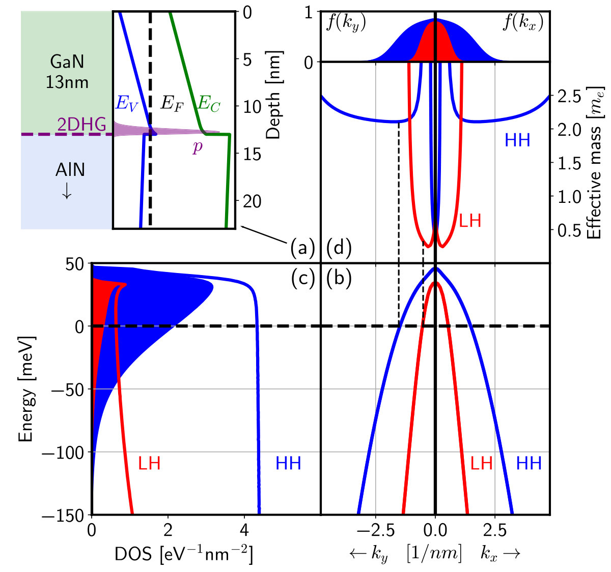 Figure 2
 Figure 3
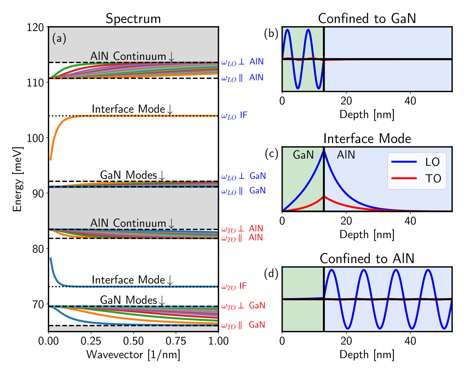 Figure 4
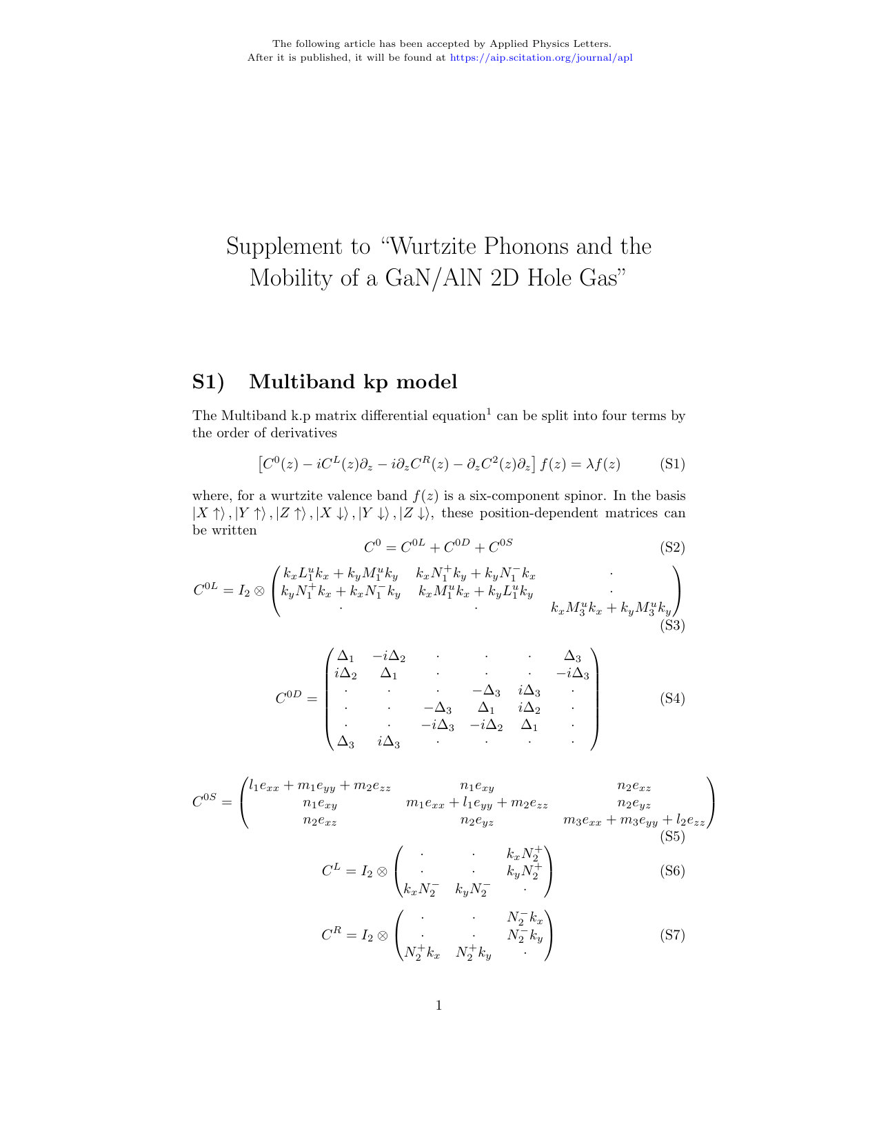 Figure 5
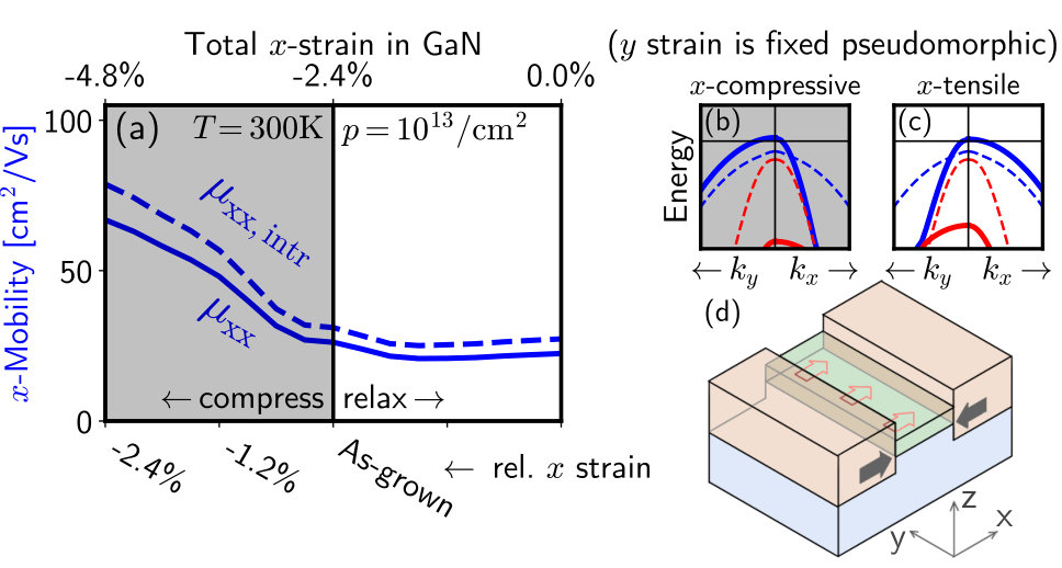 Figure 6
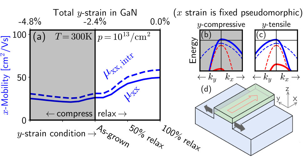 Figure 7
Peer Reviews
No public reviews on file for this paper yet. If you reviewed it on a platform where reviews are public (OpenReview, ICLR, NeurIPS, ICML), you can paste yours below so the community can read it here.
Videos
No videos yet. Explain this paper in a talk, walkthrough, or lecture? Add one.
\SetWatermarkText
The following article has been accepted by Applied Physics Letters.
After it is published, it will be found at https://aip.scitation.org/journal/apl
\SetWatermarkAngle
0 \SetWatermarkColorred \SetWatermarkLightness0 \SetWatermarkVerCenter0.5in \SetWatermarkFontSize7pt
Wurtzite Phonons and the Mobility of a GaN/AlN 2D Hole Gas
Samuel James Bader
[email protected] [ Cornell University School of Applied & Engineering Physics, Ithaca, NY USA 14853
Reet Chaudhuri
Cornell University School of Electrical & Computer Engineering, Ithaca, NY USA 14853
Martin Schubert
X Development LLC, 100 Mayfield Ave, Mountain View, CA USA 94043
Han Wui Then
Intel Corporation, 2501 NE Century Blvd, Hillsboro, OR USA 97124
Huili Grace Xing
Cornell University School of Electrical & Computer Engineering, Ithaca, NY USA 14853
Cornell University Dept. of Materials Science & Engineering, Ithaca, NY USA 14853
Kavli Institute at Cornell, Ithaca, NY USA 14853
Debdeep Jena
Cornell University School of Electrical & Computer Engineering, Ithaca, NY USA 14853
Cornell University Dept. of Materials Science & Engineering, Ithaca, NY USA 14853
Kavli Institute at Cornell, Ithaca, NY USA 14853
Abstract
To make complementary GaN electronics more than a pipe dream, it is essential to understand the low mobility of 2D hole gases in III-Nitride heterostructures. This work derives both the acoustic and optical phonon spectra present in one of the most prominent p-channel heterostructures (the all-binary GaN/AlN stack) and computes the interactions of these spectra with the 2D hole gas, capturing the temperature dependence of its intrinsic mobility. Finally, the effects of strain on the electronic structure of the confined 2D hole gas are examined and a means is proposed to engineer the strain to improve the 2D hole mobility for enhanced p-channel device performance, with the goal of enabling wide-bandgap CMOS.
Decades after the celebrated invention of Mg p-doping Nakamura et al. (1992) in Gallium Nitride (GaN) and the subsequent development of GaN-based LEDs, the manipulation of holes in GaN remains a fundamental challenge. Consequently, despite the expected dominance of GaN High Electron Mobility Transistors (HEMTs) in the coming generation of power electronics Huang (2017) and communications systemsYuk, Branner, and Cui (2017), there is no complementary p-channel device which can be readily integrated. This incompleteness restricts the possible circuit topologies and system designs acheivable in GaN electronics, but arises quite straightforwardly from the physics of the GaN valence band. These bands, both heavy and deep in energy, have proven difficult to contact with typical metal workfunctions Song, Ha, and Seong (2010), difficult to dope with high efficiency Kozodoy et al. (2000), and difficult to flow current through with high conductivity. Nonetheless, the commercial interest in generating complementary GaN-based circuits Chu et al. (2016) and scientific interest in studying highly-degenerate hole physics Chaudhuri et al. have prompted great recent progress in p-channel devices Bader et al. (2018).
Of the varied structures Shatalov et al. (2002); Zimmermann et al. (2004); Li et al. (2013); Hahn et al. (2013); Chu et al. (2016); Zhang et al. (2016); Nomoto et al. (2017); Nakajima et al. (2018); Krishna et al. (2019) which have been proposed as a platform for p-channel III-Nitride electronics, the single GaN/AlN heterojunction field-effect transistor has received recent attention for its high sheet conductance Chaudhuri et al. and excellent device performance Bader et al. (2018). In this structure, depicted in Fig 1(a), the all-binary materials provide a straightforwardly repeatable growth with no possible parasitic electron channels, a tremendous hole-inducing polarization-charge for low sheet-resistance, and maximal bandgaps for extreme voltage-handling capability. Given the recent reports of temperature-dependent transport studies in this heterostructure Chaudhuri et al. , and recent first-principles suggestions of possible enhancements to hole mobility in bulk p-GaN Ponce, Jena, and Giustino , this work presents a model to explain the measured mobility of the 2D hole gas (2DHG) at the GaN/AlN interface, and evaluates the potential of strain-engineering approaches to alter the bandstructure in a favorable way. First, the valence band structure including confinement and multi-band mixing effects are computed. Then the spectra of both acoustic and optical phonons in the heterostructure are determined and the mobility limitation due to these mechanisms is derived. Finally, the effects of strain on the band structure and mobility are presented.
The multi-band k.p (MBKP) approach, based on Burt Exact Envelope Function Theory Foreman (1993); Burt (1994), describes the electronic states of heterostructures wherein multiple subbands may be intermixed by non-uniform potentials and material interfaces. MBKP has been extended to wurtzite heterostructures by various authors Mireles and Ulloa (1999); Chuang and Chang (1996) and is available in certain commercial packages Birner (2011). The PyNitride software package Bader employed here self-consistently Tan et al. (1990) solves the 6x6 MBKP equation of the wurtzite valence band (see Supplement) simultaneously with the Poisson equation, accounting for the large fixed interface polarization charge. Figure 1(a) depicts a highly confined 2D hole gas at the GaN/AlN interface. The hole gas represents contributions mainly from the first quantized subband of both the heavy hole (HH) and light hole (LH) bands (including spin, this is four subbands). The transverse dispersion is shown in Fig 1(b). By density, as clear from Fig 1(c), the HH band dominates, though as shown in Fig 1(d), the LH band has lighter in-plane mass near the Fermi energy, so it contributes significantly to transport. To evaluate transport, we proceed to describe the phonons.
The Dielectric Continuum modelStroscio and Dutta (2004) describes polar optical phonons (POPs) in arbitrary heterostructures. As POP scattering is the main limitation on electron mobility in quality GaN, numerous authors have invested significant theoretical effort into the elaboration of POP spectra in various wurtzite heterostructures Shi (2003); Medeiros et al. (2005); Liao, Dutta, and Stroscio (2010); Komirenko et al. (1999); Zhu, Ban, and Ha (2012). A structure as simple as this, in fact, can be solved analytically. For a uniaxial crystal, the effect of polar optical phonons can be incorporated into two frequency () dependent, directional dielectric functions, and :
[TABLE]
where those longitudinal () and transverse () POP frequencies and high-frequency dielectric constant can be determined experimentally for the materials in play (see tabulation in Komirenko Komirenko et al. (1999)). For a mode with in-plane wavevector , the POP problem reduces to solving a frequency-dependent Poisson eigenvalue equation:
[TABLE]
for the potential . At every characteristic frequency appearing in Eq 1, a dielectric constant changes sign, which changes the character of the involved modes (locally decaying vs oscillating). Altogether, there are three classes of modes depending on the energy range: (1) oscillating in GaN, decaying in AlN, (2) oscillating in AlN, decaying in GaN, and (3) decaying bidirectionally from a GaN/AlN interface. For each class, both transverse and longitudinal polarizations are possible. The spectrum and example modes are depicted in Fig 3 and the solution is elaborated in the Supplementary Materials.
The Elastic Continuum model Stroscio and Dutta (2004) aptly describes acoustic phonons in arbitrary heterostructures. Given the centrality of optical phonons in electron-based devices, the literature on acoustic phonons in wurtzite heterostructures Pokatilov, Nika, and Balandin (2003, 2004); Balandin, Nika, and Pokatilov (2004); Balandin, Pokatilov, and Nika (2007) is significantly less comprehensive. The basic approach is to link a continuum Newton’s law with a material stress-strain relation:
[TABLE]
where is the local displacement vector, is the density, is the stress tensor, is the stiffness tensor, and is the strain tensor . Due to symmetry constraints on the stiffness tensor, the in-plane shear component is uncoupled (“Y” modes) while longitudinal and out-of-plane components constitute two coupled differential equations (“XZ” modes). These are solved by the Finite Element Method. For both types of modes, there are two characters possible depending on the energy range. At energies above , where is the relevant AlN sound velocity, modes are able to propagate in the AlN, and are thus of a continuum sort. Below this energy, any modes which exist must decay into the AlN, so are GaN-confined modes. The spectrum and example modes are revealed in Fig 3, and the solution methodology is elaborated in the Supplementary Materials.
We now turn to the interactions of the phonons and carriers. First, both types of phonon modes are normalizedStroscio and Dutta (2004) by the quantization condition . Once the oscillations are normalized, the Hamiltonian term for each mode can be generated. For optical phonons, this is just . For acoustic phonons, the deformation potential is a six-by-six matrix function of position: at each position it recruits the valence deformation matrix of the local material and also the local strain from a given acoustic mode. There is also a (coherently-combined) piezo term where is foundPokatilov, Nika, and Balandin (2004) by solving the Poisson equation given the piezoelectric charge induced by the mode (see Supplement). Finally, to account for the low-temperature mobility, which is around 200cm2/Vs in these structures to date, some extrinsic limitation must be included. The exact cause (e.g. interface roughness, dislocation, impurity, etc) is irrelevant to this study, since all these elastic mechanisms are temperature-independent and have similar dependence on effective masses. So the exact cause is not deduced here, but rather a generic scatterer with constant scalar matrix element is applied to set the low-temperature mobility to 200cm2/Vs. This matrix element is the only “tuning parameter.”
To calculate the perturbed carrier distribution, we employ the linear Boltzmann Transport Equation (LBTE):
[TABLE]
where is the in-plane electric field, is the equilbrium occupation function, is a small change in occupation to be solved for, and the transition rate is given by
[TABLE]
where represents absorption/emission respectively, is the state with in-plane wavevector , of subband , is the perturbation due to mode with wavevector , and / are the electronic/phonon energies. Once this is discretized on a k-space mesh, the LBTE is solved as a linear matrix equation for the change in occupation under applied field, from which the mobility is extracted. The results, Fig 4, compare agreeably to experiment over a wide temperature range, and verify Poncé’s predictionPonce, Jena, and Giustino that acoustic phonons dominate scattering at room temperature.
Now we discuss what can be done to improve the mobility. In a recent first-principles study of the mobility of bulk p-type GaN, Poncé et al Ponce, Jena, and Giustino suggested the application of significant tensile in-plane strain (or compressive c-axis strain) to raise the split-off band (SO) above the heavy-hole and light-hole bands. The lighter mass of the split-off band would allow for a drastically increased hole mobility. Such a proposal, while potentially revolutionary for bulk p-GaN, is difficult to apply to the particular heterostructure discussed here-in, since the GaN-pseudomorphic-to-AlN is already compressively strained by 2.4% as-grown, and that large strain would have to be overcome first before applying further tensile strain. Moreover, applying tensile strain dramatically changes the interface between GaN and AlN, significantly reducing the valence band offset (VBO) and thus the confining potential. [The role of strain in the asymmetry of the GaN/AlN and AlN/GaN VBO is well-known Vurgaftman and Meyer (2003).]
This raises the question of whether reasonable strain can improve the mobility of holes in this heterostructure, without access to the deep SO band. Based on the theory of Suzuki and Oenoyama Suzuki and Uenoyama (1996) in the context of lasers, two converse techniques may be suggested employing strain along only one in-plane axis. Dasgupta et al Dasgupta, Radosavljevic, and Then (2017) considered the application of compressive strain along the direction of current flow. Conversely, Gupta et al Gupta et al. (2018) tested the application of tensile strain perpendicular to current flow. Figures 6 and 6 consider what effects these two proposals have, not on bulk p-GaN as with previous authors, but rather on the heterojunction band structure. To take full advantage of the changing band structure near the band edge, the charge density is lowered [by thinning the well layer to 8nm] and kept constant at by variable applied bias even as the strain is changed. These adjustments to thickness and charge match closely the actual 2DHG environment in p-channel FETs Bader et al. (2018). In parts (b) and (c) of these figures, uniaxial in-plane strain is seen to split the topmost two-bands. Depending on the sign and orientation of the strain, the topmost band may become light or heavy in the current flow direction ().
In the case of tensile -strain, Fig 6(c), or compressive -strain, Fig 6(b), the topmost band is heavy along , so, even though the available scattering DOS is reduced by the band-splitting, the net mobility remains low. However, in the case of compressive -strain, Fig 6(b), or tensile strain, Fig 6(c), the topmost band is light along and interband scattering is diminished. As such, these strain conditions result in an enhance mobility. The mobility improvement due to -compressive strain is more pronounced than -tensile strain because of the aforementioned effect which tensile strain has on the VBO. However, these two enhancement mechanisms are not mutually exclusive: a fin relaxation and a compressive regrowth would complement each other via the Poisson effect to reduce the total amount of stress which each mechanism would have to apply.
Of course, any enhancements will still be limited by whatever extrinsic mechanisms are at play, so Figs 6 & 6 include two mobility curves: (1) a (solid blue) prediction which assumes the extrinsic scattering element is similar to the present data and (2) a (dashed blue) intrinsic calculation using only phonon mechanisms, corresponding to space for further improvements in growth.
In conclusion, this work has combined solutions for both the optical and acoustic phonon spectra in a GaN/AlN heterostructure with a multiband description of the hole gas to model the hole mobility. The model qualitatively matches experimental observations and can be used to estimate what sort of intrinsic mobility enhancements are possible by strain engineering, suggesting that a unixial compression is the best approach for optimizing the GaN/AlN hole gas. A high-mobility 2DHG could join the celebrated GaN 2DEG to realize a future of energy-efficient complementary GaN-based circuits.
Supplementary Material
See the Supplementary Material for mathematical and numerical simulation details.
Acknowledgements.
Work supported by Intel Corp, by AFOSR Grant FA9550-17-1-0048, and by NSF Grants 1710298/1534303. Authors appreciate discussions with Samuel Poncé, Feliciano Giustino, Tomás Palacios, Nadim Chowdhury, Paul Fischer and Sansaptak Dasgupta.
The reference list from the paper itself. Each links out to its DOI / PubMed record.
- 1Nakamura et al. (1992) S. Nakamura, T. Mukai, M. Senoh, and N. Iwasa, “Thermal Annealing Effects on P-Type Mg-Doped Ga N Films,” Japanese J. App. Phys. 31 , L 139 (1992) . · doi ↗
- 2Huang (2017) A. Q. Huang, “Wide bandgap (WBG) power devices and their impacts on power delivery systems,” Technical Digest - Intl. Electron Devices Meeting, IEDM , 20.1.1.1.4 (2017) . · doi ↗
- 3Yuk, Branner, and Cui (2017) K. Yuk, G. R. Branner, and C. Cui, “Future directions for Ga N in 5G and satellite communications,” Midwest Symposium on Circuits and Systems 2017 , 803 (2017) . · doi ↗
- 4Song, Ha, and Seong (2010) J. O. Song, J. S. Ha, and T. Y. Seong, “Ohmic-contact technology for Ga N-based light-emitting diodes: Role of p-type contact,” IEEE Transactions on Electron Devices 57 , 42 (2010) . · doi ↗
- 5Kozodoy et al. (2000) P. Kozodoy, H. Xing, S. P. Den Baars, U. K. Mishra, A. Saxler, R. Perrin, S. Elhamri, and W. C. Mitchel, “Heavy doping effects in Mg-doped Ga N,” J. App. Phys. 87 , 1832 (2000) . · doi ↗
- 6Chu et al. (2016) R. Chu, Y. Cao, M. Chen, R. Li, and D. Zehnder, “An Experimental Demonstration of Ga N CMOS Technology,” IEEE Elec. Dev. Lett. 37 , 269 (2016) . · doi ↗
- 7(7) R. Chaudhuri, S. J. Bader, Z. Chen, D. A. Muller, H. G. Xing, and D. Jena, “A polarization-induced 2D hole gas in undoped gallium nitride quantum wells,” Unpublished (in review) ar Xiv:1807.08836 .
- 8Bader et al. (2018) S. J. Bader, R. Chaudhuri, K. Nomoto, A. Hickman, Z. Chen, H. W. Then, D. A. Muller, H. G. Xing, and D. Jena, “Gate-recessed E-mode p-channel HFET with high on-current based on Ga N/Al N 2D hole gas,” IEEE Elec. Dev. Lett. 39 , 1848 (2018) . · doi ↗