Topologically protected wave packets and quantum rings in silicene
B. Szafran, B. Rzeszotarski, A. Mre\'nca-Kolasi\'nska

TL;DR
This paper investigates topologically protected chiral wave packets in silicene, demonstrating their stable propagation, valley transitions, and quantum interference effects in a proposed quantum ring structure.
Contribution
It introduces a detailed atomistic and analytical study of wave packet dynamics and interference in silicene, including the design of a quantum ring with observable Aharonov-Bohm oscillations.
Findings
Wave packets move with constant velocity and shape preservation.
Backscattering occurs during valley transitions.
Aharonov-Bohm oscillations are observed in conductance.
Abstract
We study chiral wave packets moving along the zero-line of a symmetry breaking potential of vertical electric field in buckled silicene using an atomistic tight-binding approach with initial conditions set by an analytical solution of the Dirac equation. We demonstrate that the wave packet moves with a constant untrembling velocity and with a presevered shape along the zero line. Backscattering by the edge of the crystal is observed that appears with the transition of the packet from to valley or vice versa. We propose a potential profile with branching of the flip line that splits the wave packet and produces interference of the split parts that acts as a quantum ring. The transition time exhibits Aharonov-Bohm oscillations in the external magnetic field that are translated to conductance oscillations when the intervalley scattering is present within the ring.
Click any figure to enlarge with its caption.
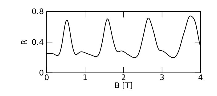 Figure 1
 Figure 2
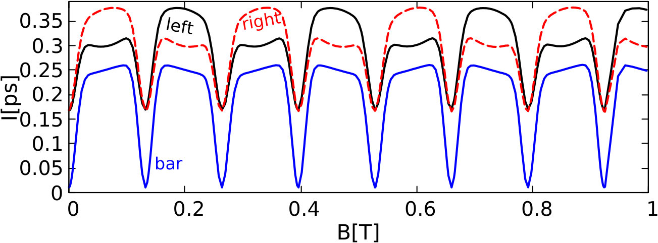 Figure 3
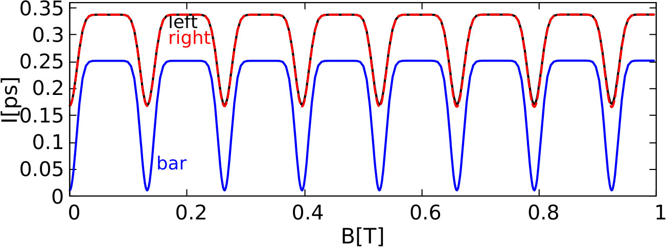 Figure 4
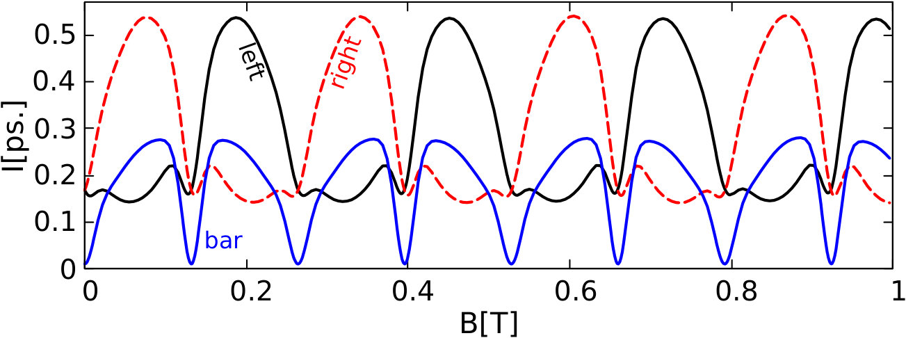 Figure 5
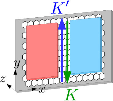 Figure 6
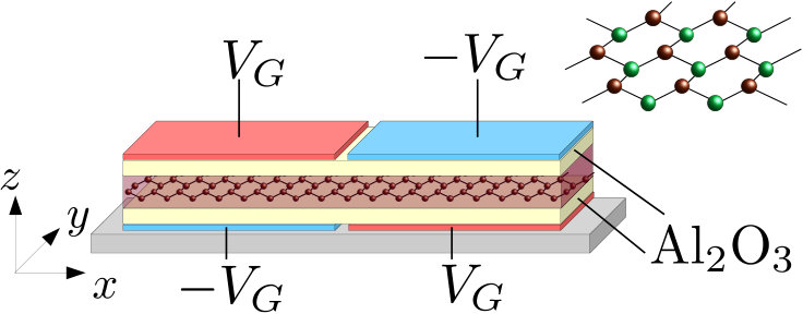 Figure 7
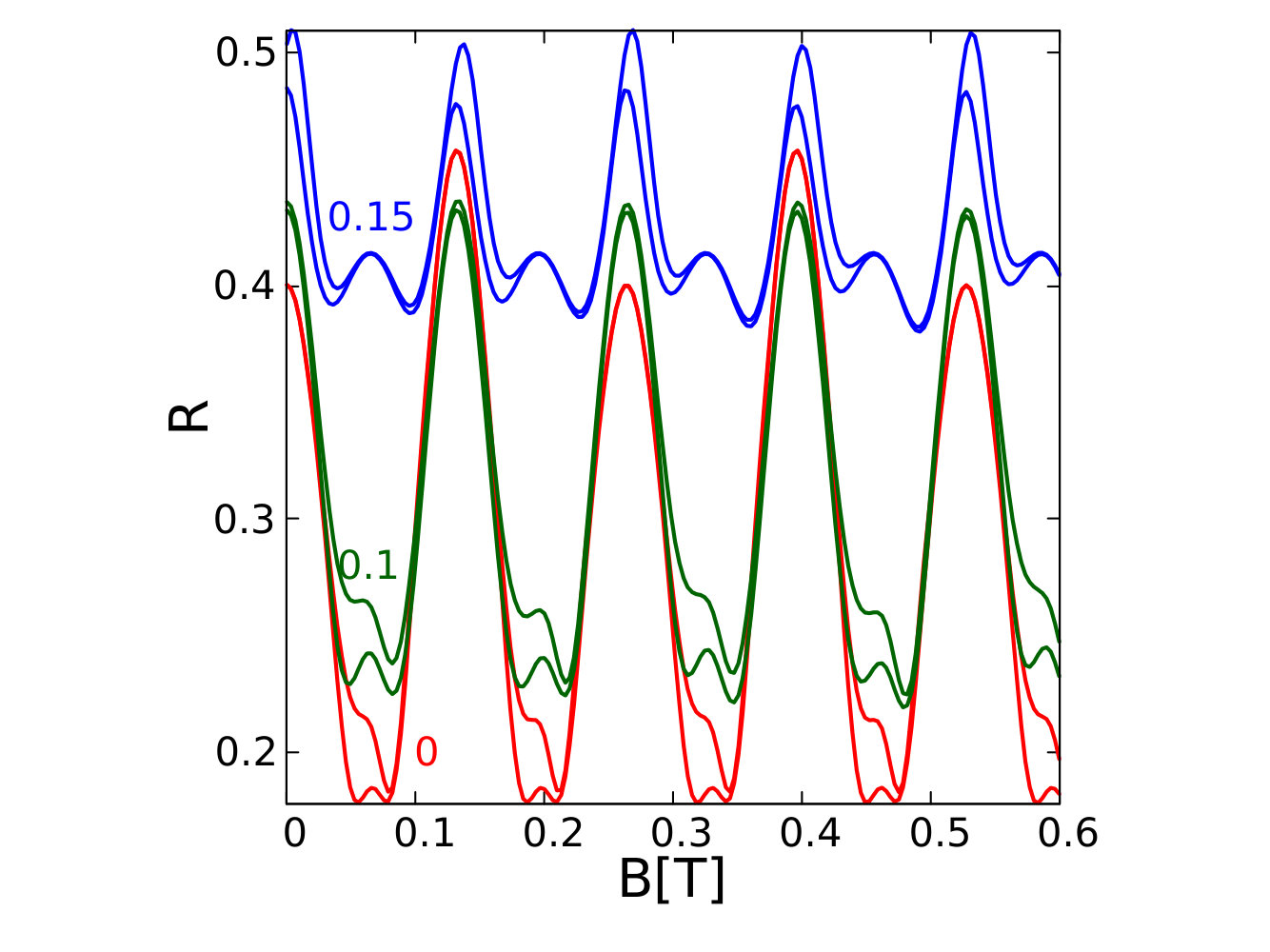 Figure 8
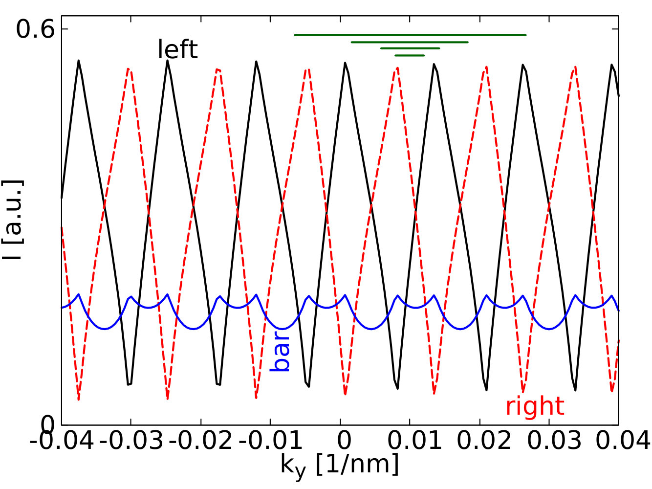 Figure 9
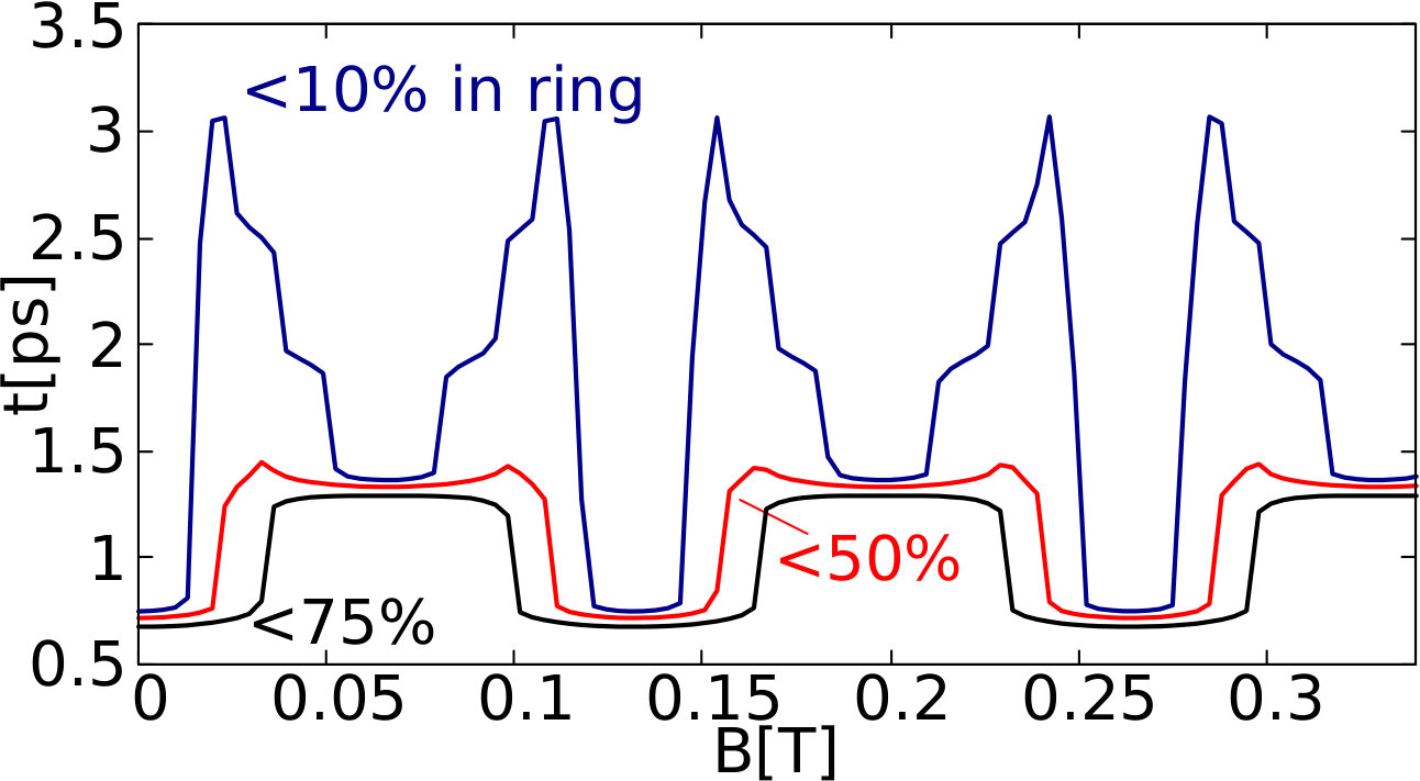 Figure 10
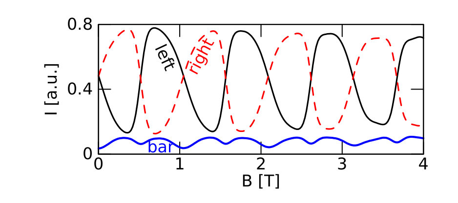 Figure 11
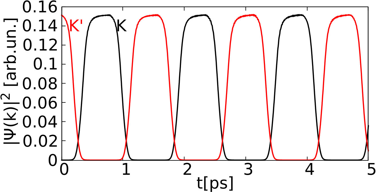 Figure 12
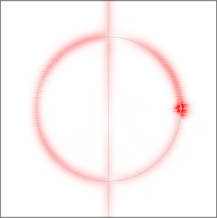 Figure 13
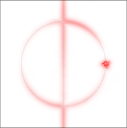 Figure 14
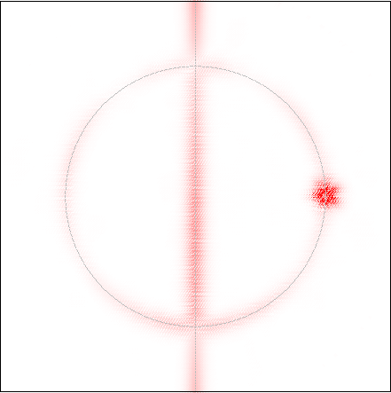 Figure 15
 Figure 16
 Figure 17
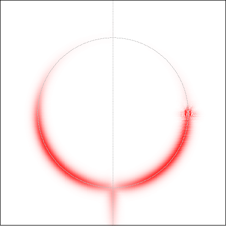 Figure 18
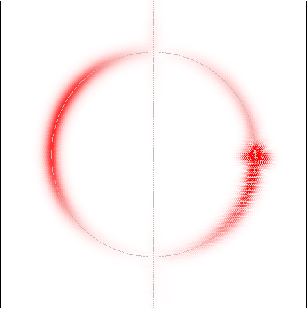 Figure 19
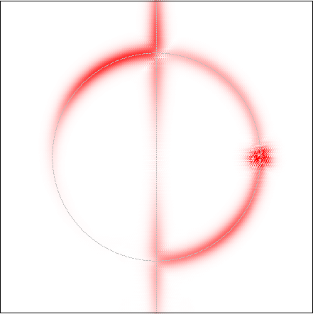 Figure 20
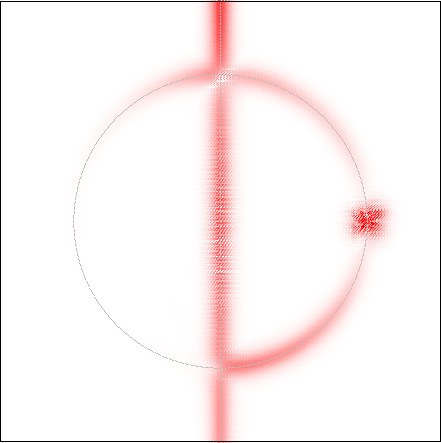 Figure 21
 Figure 22
 Figure 23
 Figure 24
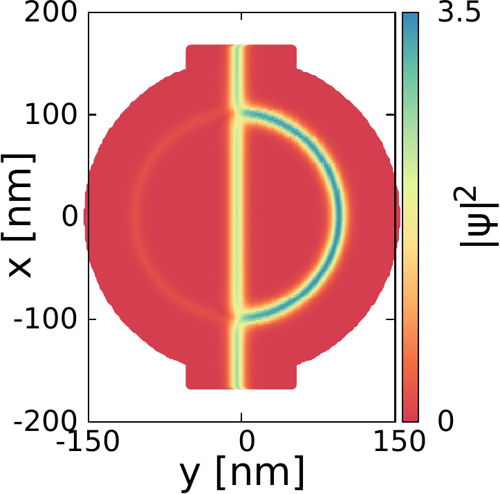 Figure 25
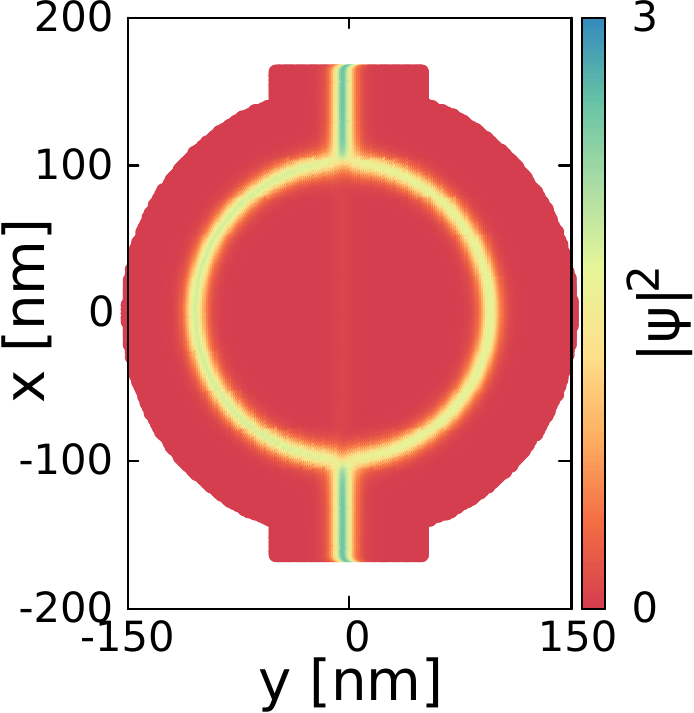 Figure 26
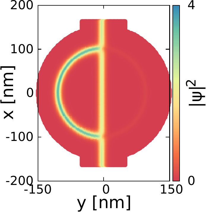 Figure 27
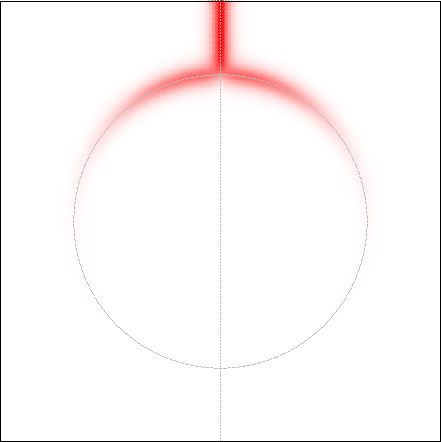 Figure 28
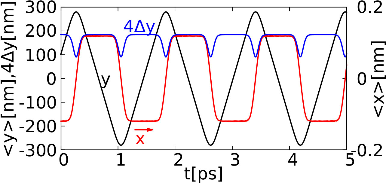 Figure 29
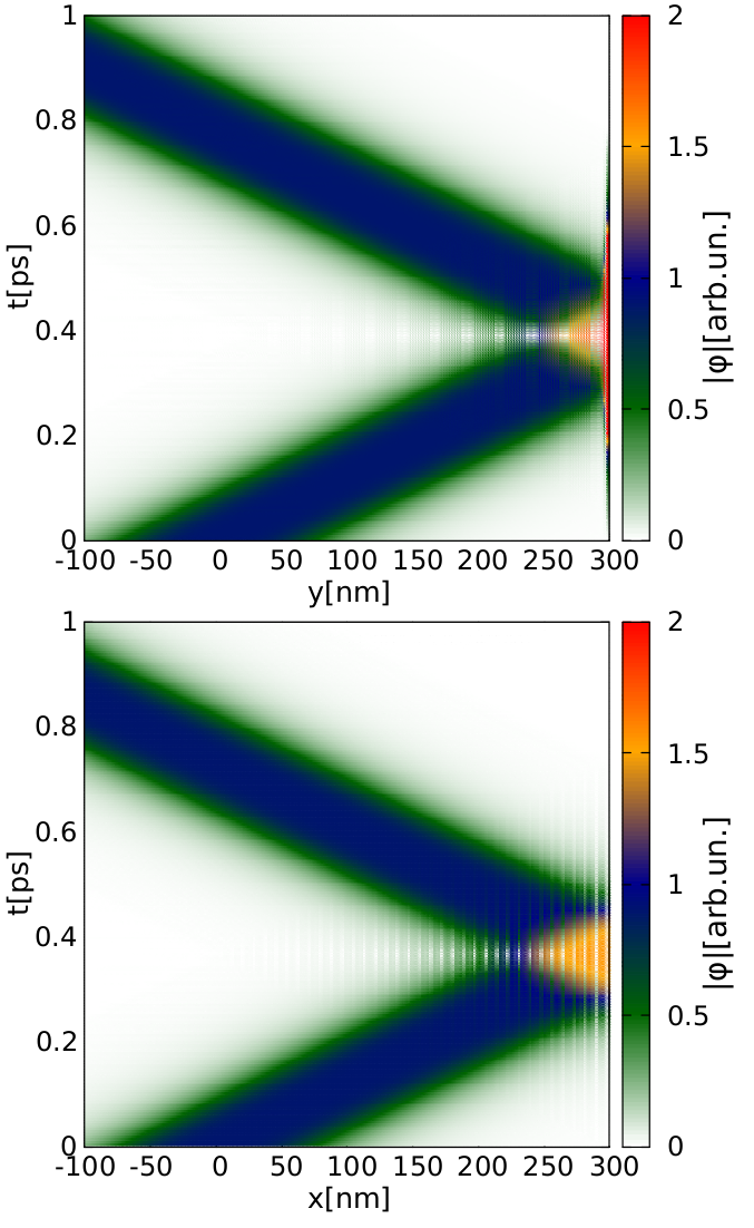 Figure 30
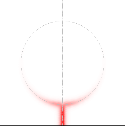 Figure 31
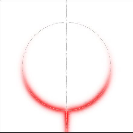 Figure 32
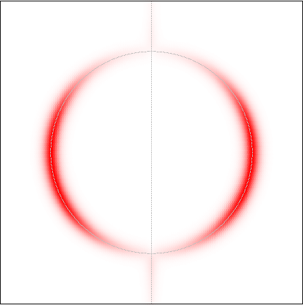 Figure 33
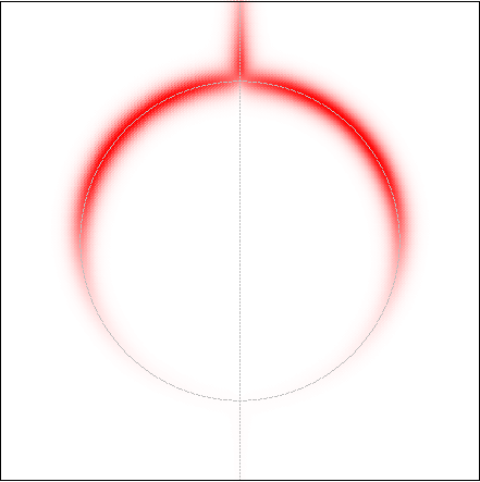 Figure 34
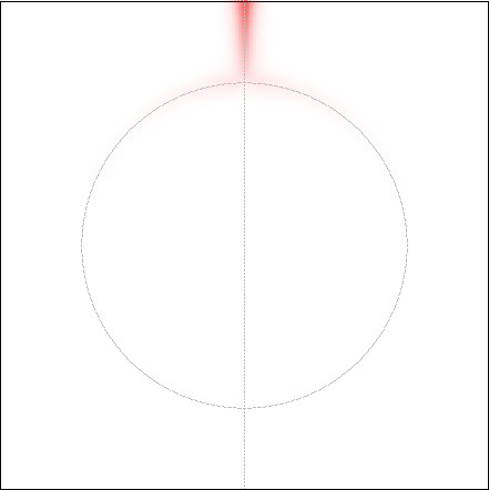 Figure 35
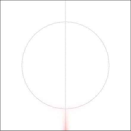 Figure 36
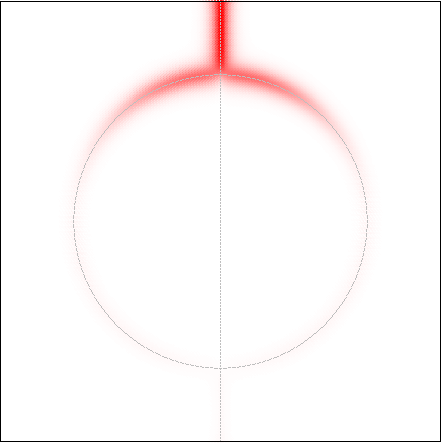 Figure 37
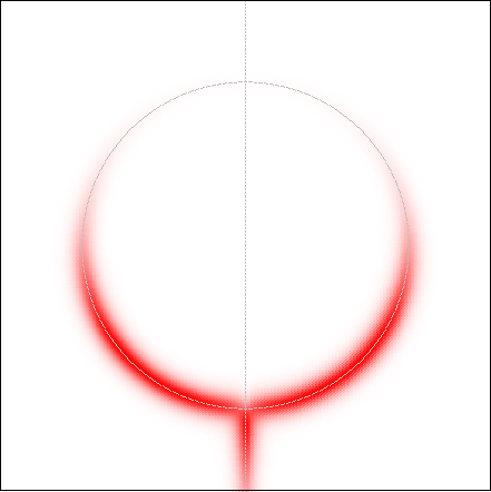 Figure 38
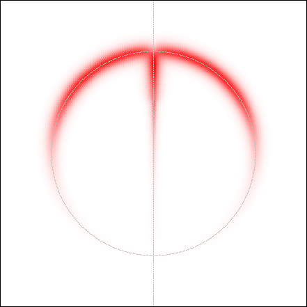 Figure 39
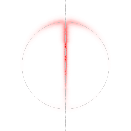 Figure 40
Peer Reviews
No public reviews on file for this paper yet. If you reviewed it on a platform where reviews are public (OpenReview, ICLR, NeurIPS, ICML), you can paste yours below so the community can read it here.
Videos
No videos yet. Explain this paper in a talk, walkthrough, or lecture? Add one.
Topologically protected wave packets and quantum rings in silicene
Bartłomiej Szafran, Bartłomiej Rzeszotarski, and Alina Mreńca-Kolasińska
AGH University of Science and Technology, Faculty of Physics and Applied Computer Science,
al. Mickiewicza 30, 30-059 Kraków, Poland
Abstract
We study chiral wave packets moving along the zero-line of a symmetry breaking potential of vertical electric field in buckled silicene using an atomistic tight-binding approach with initial conditions set by an analytical solution of the Dirac equation. We demonstrate that the wave packet moves with a constant untrembling velocity and with a preserved shape along the zero line. Backscattering by the edge of the crystal is observed that appears with the transition of the packet from to valley or vice versa. We propose a potential profile that splits the wave packet and next produces interference of the split parts that acts as a quantum ring. The transition time exhibits Aharonov-Bohm oscillations in the external magnetic field that are translated to conductance oscillations when the intervalley scattering is present within the ring. We study wave packet dynamics as function of the width of the packet to the limit of plane waves. In the stationary limit the conductance oscillation period is doubled and the scattering density oscillates between the left and right arms of the ring as function of the magnetic field. We demonstrate that this effect is also found in a quantum ring defined by the zero lines in bilayer graphene.
I Introduction
In monolayer honeycomb materials, including graphene gra , Xenes Molle17 (silicene Aufray10 ; Liu11 , germanene cha ; Liu11 , stanene sta ), transition metal dichalcogenides tmdc , or bismuthene Reis17 , the Fermi level appears in two non-equivalent valleys of the Brillouin zone. In graphene ribbons nrbr with zigzag edges there is a strict correspondence between the valley state and the direction of the current flow zz1 ; zz2 ; zz3 . The valley protects the chiral chiral electron transport from backscattering by long range potential disorder, which led to the valley electronics rycerz ; ryre or application of the valley degree of freedom to information processing ryre ; vq1 ; vq2 .
In bilayer morpugo and staggered monolayer graphene niu a topological confinement inside the sample, far from the edges, was found morpugo ; niu along a zero line of inversion-symmetry-breaking potential. For bilayer graphene bgr this potential is introduced by an electric field perpendicular to the layers morpugo . The bias opens the energy gap in the band structure bgr ; wry . For an inhomogeneous electric field that is inverted at the zero line in space, topologically protected chiral currents have been found morpugo confined in space to a region of the electric field flip. The flip line provides a one-dimensional confinement or quantum-wire-type channels macdo ; peet ; muktu ; muktu2 . The one-dimensional confinement of currents is also found in the quantum Hall conditions at the n-p junctions np induced by electric fields. In contrast to the currents localized at the n-p interface rick ; tay ; snejk , the confinement in zero-line channels does not require external magnetic field morpugo . Note, that formation of an energy gap was also found in epitaxial monolayer graphene due to the sublattice symmetry breaking by the substrate sic . However, the gap of this origin cannot be easily inverted for the topological confinement.
A perpendicular electric field opens the energy gap for the buckled Xenes monolayers Molle17 ; ni ; Drummond12 , and an inversion of the field induces topological confinement similarly as in bilayer graphene Ezawa12a . In contrast to bilayer graphene, (i) in Xenes the chiral energy level that passes from the valence to the conduction band is a linear function of . In Xenes a (ii) single topological state per current direction is present instead of two as in bilayer graphene. As a consequence of (i) and (ii) the wave packet formed at zero line in a Xenes should be stable against excitations and should travel with a constant shape due to independence of the velocity on the wave vector.
In this paper we study the dynamics of the chiral wave packets along the zero lines of the electric field in silicene Molle17 ; rivi ; chow ; Ezawa ; s1 ; s2 ; s3 , which is the most advanced Xenes material, with a successful application for the field effect transistor Tao15 . The chiral wave packets move with the Fermi velocity and the motion of the topological packets is free from Zitterbewegung ci2 ; citer ; frolo ; naturd which is characteristic to the solution of the Dirac equation and was found also for Weyl fermions in graphene citer ; rome ; frolo . Moreover, the topological electron packets move with a constant shape, similarly to solitons, that in other conditions require interaction with the environment – see the electron solitons self-focused with interaction to the metal gates in heterostructures bed or the Trojan wave packets formed by carefully prepared electromagnetic field tro1 ; tro2 .
We show that the chiral electron packets can be transferred from one valley to the other by backscattering from the edge of the crystal and we find that the packet appears in the opposite valley in a restored shape. Potential profiles that act as beam splitters and quantum rings qr are proposed. An interference of the split parts of the wave packet can be controlled by external magnetic field threading the quantum ring. The ring stores the wave packet for a time that is a periodic function with the period the flux quantum. The Aharonov-Bohm ab conductance oscillations are also demonstrated for the system with an intervalley scattering present. The topological rings are a new form of quantum rings for Dirac electrons, with respect to previously considered systems with structural confinement structure0 ; structure ; structure2 ; structure3 ; structure4 , mass confinement massconf ; massconf2 ; massconf3 or the confinement at circular n-p junctions in the quantum Hall conditions amk .
In the long wave packet limit, i.e. when the width of the packet is comparable with the diameter of the ring, the interference within the ring is translated into an imbalance of the scattering density in the left and right arms of the ring that becomes a periodic function with doubled Aharonov-Bohm period. The result is also found in the stationary transport for silicene and bilayer graphene.
This paper is organized as follows. In Section II we provide an analytic solution to the Dirac equation for the topologically protected currents at the inversion of the electric field (II.A). In section II.B the solution of the continuum approximation (II.A) is translated to atomistic tight-binding description which naturally accounts for the intervalley scattering, and the time stepping procedure is explained. In the Section III we test the stability of the wave packet against the intervalley transition (III.A) and describe the Aharonov-Bohm ab oscillations of the electron storage time by the ring (III.B). Section III.C describes the conductance oscillations for intervalley scattering within the ring. The long wave packet limit is disussed in III.D, and the limit is confronted with the standard calculation based on the stationary electron scattering in Section III.E. Section III.F shows the results of the Landauer approach for quantum rings defined by the zero lines in bilayer graphene. Section IV contains the summary.
II Theory
II.1 Chiral currents confined by the energy gap inversion
The chiral currents at the band inversion in silicene similar to the ones in bilayer graphene morpugo were found in Ref. Ezawa12a . For buckled monolayers as well as for bilayer systems the energy gap can be tailored in space using multiple split gates with inverted polarization. The idea of the local manipulation of the energy gap by dual split gates was proposed for topological confinement morpugo and pseudospin electronics in bilayer systems re2a ; re2b ; re2c .
Here, we consider a buckled silicene monolayer sandwiched in between top and bottom gates [Fig. 1(a,b)]. The gates are split, so that the electric field changes orientation along the axis (i.e. for ). We model the potential at the A sublattice using an arctangent function
[TABLE]
We assume that the silicene is embedded symmetrically between the gates, so that on the B sublattice we have [Fig.1(c)]. The potential bias between the sublattices opens an energy gap in the band structure ni ; Drummond12 . For potential of Eq. (1) the energy gap is inverted at by the flip of the electric field orientation.
For the wave function components defined on sublattices the low-energy approximation to the atomistic tight-binding Hamiltonian reads Ezawa12a
[TABLE]
where is the valley index ( for the valley and -1 for the valley), , and are the Pauli matrices in the sublattice space, , the Fermi velocity is determined by the nearest distance between Si atoms Å and the tight-binding hopping parameter eV Liu11 ; Ezawa . In Eq. (2) meV is the intrinsic spin-orbit coupling constant Liu11 ; Ezawa . The intrinsic spin-orbit coupling is diagonal in the basis of eigenstates of the component of the spin and is treated as a quantum number.
With potential given by Eq. (1) the Hamiltonian commutes with the operator. The common eigenfunctions of the energy and momentum component can be put in form . The Hamiltonian eigenfunctions fulfill the system of equations
[TABLE]
where the prime stands for derivative. We plug in Eqs. (3,4) a relation , i.e. a guess based on a numerical solution that allows us to derive an analytical solution for states localized near the zero-line area. A sum of the resulting equations relates the potential and the wave function
[TABLE]
For the specific form of potential given by Eq. (1) the (unnormalized) wave function is found by a standard integration technique
[TABLE]
The term in the exponent for low introduces a Gaussian-like dependence to the wave function and keeps it localized near the band inversion area [Fig. 1(c)]. The average value of for , 2, 4, 12, and 20 nm is 2.45, 2.87, 3.55, 5.45 and 6.83 nm, respectively. In presence of the spin-orbit coupling the wave function is not ideally symmetric with respect to the center of the gap inversion line: the term including the spin-orbit coupling shifts the wave function at left (right) of the inversion line for negative (positive) product of valley index and the eigenvalue. For the applied parameters these shifts are not very strong – see the blue and red lines in Fig. 1(c). In the calculations below we set .
The energy of the states localized at the gap inversion can be calculated by adding Eqs. (3) and (4) still with the relation , which gives
[TABLE]
The entire dispersion relation calculated numerically with a finite difference approach sweep is given in Fig. 1(d). The linear band energy is independent of the or which only affect the transverse wave function localization at the energy gap inversion line. Above the energy gap a continuous spectrum is found with a parabolic threshold as a function of . Near the zero energy only the localized reflectionless currents flow, and for meV, the gap is wide enough to make the currents stable at room temperature. For the Fermi wave vector nm*-1* ( meV) the continuum appears still 100 meV above the linear band.
The sign of the electron velocity within the linear band depends on the valley index. Hence, the transport at the inversion line is chiral, i.e. the electron states of the valley () go up (down) along the electric field flip line [Fig. 1(b)]. Generally, in the states localized along the field flip the current in the () valley flows with the negative (positive) potential at the A sublattice at the left-hand side.
II.2 Chiral solitons in the atomistic tight-binding
II.2.1 Atomistic Hamiltonian
Since the electron velocity in the linear chiral band is independent of the wave packet localized at the flip of the electric field should move with an unchanged shape along the line. The description of the electron wave packets stabilized by the valley degree of freedom calls for an approach that takes into account the intervalley scattering. A natural choice is the atomistic tight-binding approach. The positions of the ions of the A sublattice are generated with the crystal lattice vectors and , where Å is the silicene lattice constant, and , are integers. The B sublattice ions are generated by , with the vertical shift of the sublattices Å. The coordinates of the center of the valleys in the reciprocal space are rivi . The valleys for (-1) are referred to as ().
We use the Hamiltonian Liu ; Ezawa ; chow
[TABLE]
where stands for the nearest neighbor ions, for the next-nearest-neighbor ions. For the potential we take or . The sign is plus (minus) for the next nearest neighbor hopping path via the common neighbor ion that turns counterclockwise (clockwise). In Eq. (8) is the Peierls phase , where is the vector potential, and is the value of the magnetic field that is oriented perpendicular to the silicene plane. The last term in Eq. (8) is the spin Zeeman term with the Landé factor , and Bohr magneton .
II.2.2 Initial condition and the time-stepping
In the calculations to follow for the initial condition we use the solution of the continuum Hamiltonian [Eq. (2)] and localize the packet along the band inversion using an envelope of form , with nm and that sets the center of the packet. We set the valley momentum with a plane wave and the or coordinates. Accordingly, for the atoms of the A sublattice we set as the initial condition
[TABLE]
where is the wave vector of the packet calculated with respect to the valley center, and is given by Eq. (6). For the atoms on the sublattice we take
[TABLE]
where . We set unless stated otherwise.
We solve the Schrödinger equation on the atomic lattice , using the time step of atomic units or ps. The wave function at the first step is calculated with the implicit Crank-Nicolson scheme The subsequent time steps are calculated with the explicit Askar-Cakmack scheme . In presence of the external magnetic field the eigenstates of (3,4) need to be calculated numerically sweep . However, for the discussed range of the magnetic field ( T) and the applied narrow flip area ( nm) no significant difference between the numerical eigenstates and formula of Eq. (6) used for the initial condition were found in the wave packet evolution.
III Results
III.1 Wave packet motion
We first consider a square flake nm nm nm nm with a zigzag edge at nm and and armchair edge at nm. The packet is set in the valley () to make it move upwards (to increasing values – see Fig. 1(b)). Figure 2(a) shows the cross section of the packet along the line. The packet indeed moves up in a stable form until it reaches the zigzag edge of the flake.
The same result – as long as the packets does not reach the edge – is obtained for the solution of the time dynamics with the continuum Hamiltonian [by Eq.(2)]. The absence of Zitterbewegung ci2 ; citer ; frolo ; naturd for the wave packet that follows the Dirac equation calls for a comment. The velocity operator is obtained as citer . For the Dirac equation this operator does not commute with the Hamiltonian which is usually invoked in the interpretation of the trembling motion citer . However, the wave function localized at the zero-line that follows the specific form used in Section II.A happens to be an eigenfunction of the operator, with the eigenvalue . By, the Ehrenfest theorem for we have .
III.2 Backscattering by the flake edge
The zigzag edge of the crystal supports edge localized states. The incident packet couples to these states and in Fig. 2(a) we find formation of a high peak of the absolute value of the wave function (see the red region at the right edge of the plot for 0.4 ps). The packet is backscattered and moves to the left with a shape restored to its original form, only in the opposite direction.
The average position , , and the size of the packet along the junction is plotted in Fig. 3(a). The system is the same as in Fig. 2(a) only the packet is started at nm. In Fig. 3(b) we additionally plot the square of the absolute value of the Fourier transform of the wave packet calculated for and valleys,
[TABLE]
for (i.e. the valley) and ( valley). We find that as the packet reaches the edge of the flake it is scattered to the other valley that makes it travel in the opposite direction. In Fig. 3(a) we can also see that the average oscillates with a small magnitude which results from the valley flips at the backscattering by the edge which changes the sign of the exponent with in the wave function ( is set to 1).
We find that the restoration of the soliton upon scattering is observed for both the armchair and the zigzag termination of the flake. For backscattering by the armchair edge we flipped the potential by angle. The packet which is still started in the valley moves toward larger values until it reaches the edge [Fig. 2(b)]. Here no peak of the wave function at the edge is observed since the armchair termination does not support the edge localized states Wakabayashi2010 .
III.3 Quantum ring
A form of a quantum ring with the chiral waveguides for the electron flow can be defined with an engineering of the electric field. For that purpose one needs a local inversion of the electric field which requires additional top and bottom gates in the system. Here we consider a circular area of radius , and set the model potential at the sublattice to
[TABLE]
where nm is the circle radius with the center at the origin and is the distance from the origin. The potential at the sublattice is plotted in Fig. 4. As above we take . Fig. 4 shows also the direction of the flow for currents in the valley – with the negative (positive) potential at left (right) side of the current flow. When the line of meets the ring at nm the current can go to either the left or the right arm of the ring. This potential profile introduces a beam splitter for the electron wave packet in this way. The central bar of the ring is inaccessible for the current going up.
In quantum rings qr Aharonov-Bohm ab oscillations of coherent conductance are observed that in the Landauer-Büttiker labu approach are explained as due to variation of the electron transfer probability across the ring with phase shifts accumulated from the vector potential of the magnetic field. In the present system the electron backscattering from the ring is prohibited by the topological protection of the valley current, so the transfer probability of the soliton packet is 1 for any magnetic field. However, we find that the time that the electron spends within the ring changes due to the phase shifts introduced by the vector potential.
In this section and in the rest of the paper we neglect the intrinsic spin-orbit coupling () that introduces a weak asymmetry in the electron injection to the ring due to the spin-valley dependent shift off the zero line [cf. Fig. 3(a) and Eq. (6)]. The calculations for the quantum ring require long leads to prevent return of the packet to the scattering area upon reflection from the edge of the crystal. For long wave packets the entire computational box is taken long up to 6 m. Systems these long are treated with the scaling method of Ref. scaling for which the crystal constant is scaled as with the hopping parameter . In Hamiltonian (8) replaces , and replaces while the Si ions are generated in the computational box. We use the scaling factor or in the calculations for silicene below.
Figure 5(a) shows the snapshots of the simulation of the packet transfer across the ring for . For the packet is started 350 nm below the center of the ring of radius 100 nm. The snapshots taken at 0.204 ps and 0.325 ps show that the packet is split into two parts at the entrance to the ring. In both the left and right arms of the ring the current moves up leaving the negative potential at the A sublattice at the left-hand side [see Fig. 4]. The split packets meet at the exit of the ring [ ps and ps] with the same phase and the packet of its original size is restored [ ps].
Figure 6(a) shows the parts of the packet before ("b4", black lines) the ring, within ("in", blue lines), as well as the transferred part ("passed", red lines) as a function of time. The results for that correspond to Fig. 5(a) are plotted with the solid lines. For ps the entire packet is transferred above the ring.
In Fig. 5(b) we plotted the snapshots of the simulation for T which corresponds to half the flux quantum threading the ring with nm. The parts of the packet that meet at the exit ( ps) acquire a relative phase due to the Aharonov-Bohm effect. A node of the wave function is formed at the exit to the upper channel. A nondestructive interference is observed within the area below the exit from the ring, which directs the packet to the internal bar within the ring (ps), i.e. to the only path where the current can go for the exit to the upper channel blocked by the Aharonov-Bohm effect. The bar is transparent for the current going down [Fig.4]. The packet is split again to the left and right arms of the ring at ps. After the second round the parts of the packet meet in phase at the exit and the packet smoothly leaves the ring [ ps, ps].
In Fig. 6(a) the results for half the flux quantum are plotted with the dotted line. The packet is transferred to the exit with a delay but completely and in a single move. For comparison in Fig. 6(a) the results for the magnetic field of T which corresponds to are plotted with the dashed lines. Here a part of the packet passes to the exit as fast as for , but due to a phase difference at the exit a part of the packet stays inside the ring and leaves it in portions at subsequent rounds, which produces the steps in the dashed lines in Fig. 6(a).
In Fig. 6(b) we plotted the moments in time for which less than 75%, less than 50% and less than 10% stays within the ring as a function of the external magnetic field. The plot is periodic with the Aharonov-Bohm period of T. The ring is emptied the fastest for the integer and half quanta. The result of Fig. 6(a) for T corresponds to a local maximum of the time for which more than 10% of the packet stays within the ring. Finally Fig. 6(c) shows the part of the packet contained within the ring for a fixed moment in time as a function of the magnetic field. For ps and ps the ring-confined part is locally maximal for the magnetic field corresponding to odd multiples of half the flux quantum T. For longer times these maxima are turned into minima due to compensation of the phase difference after the second round of electron circulation [Fig. 5(b)] within the ring.
III.4 Intervalley scattering and conductance oscillations
For the potential profile plotted in Fig. 4 the transfer probability can fall below 1 only provided that a intervalley transition is present within the ring. The intervalley scattering is introduced by potential variation that is short on the atomistic scale. For the modeling we introduced a point potential defect of a Lorentzian form
[TABLE]
where , and eV and nm. In the scaling approach scaling the smooth potential that changes slowly on the atomic scale, in particular the one given by Eq. (1) and (12) stays invariant with . For the abrupt short-range defect potential we found that scaling of with is necessary to keep the same effectiveness of the intervalley scattering. The defect potential enters with the same sign to potential on both sublattices, as on sublattice A and on sublattice B.
In presence of the defect, the results start to change significantly with . The backscattering probability as a function of the external field is given in Fig. 7 for , /nm and /nm. For each value of two lines are plotted, which are the minimal and maximal bound for the backscattering probability. The difference between the two is determined by the part of the electron packet that stays within the ring at the end of the simulation (6.1 ps). as a function of is approximately periodic with the flux quantum.The behavior of the electron packet is displayed in Fig. 8 for and /nm. The packet is incident in the valley. For ps we spot the scattering center near . A part of the packet passes across the defect moving still in valley, and a larger part is backscattered and move in the direction which is only allowed for the valley. For ps the current reaches the entrance to the ring, a part of it is backscattered to the input channel, and another goes up along the bar. The electron packets of opposite valley meet within the bar for ps and 0.87 ps. For ps we can see recycling of currents for both the valleys: the valley current cannot pass to the output channel and the one to the input channel. The opposite valley currents meet again, this time in the arms of the ring for ps. For ps the packet distribution is similar to ps, only a smaller portion of the electron packet is still present within the ring.
III.5 The limit of long wave packets
The wave packet dynamics in the limit of a large size of the packet should approach the conditions of the stationary electron flow. In order to study the limit of a plane incident wave we consider a Gaussian envelope of the packet, i.e. in the initial condition given by Eqs. (9) and (10) we set . The Fourier transform of the packet produces the probability density with the standard deviation of in the wave vector space.
We solve the time evolution and integrate the parts of the packet in the left and right arms of the ring and in the center bar over time as the packet transfers the ring. In Fig. 9 we plot the results for increasing length of the packet in the initial condition. The results for nm and nm are nearly identical. The packet passess equally through the left and right arms of the ring. The integrals in Fig. 9(a) and Fig. 9(b) are periodic functions of the magnetic field with the quantum of the flux threading the ring of radius nm, i.e. T, as above. However, an asymmetry of the electron transfer across the arms appears for nm [Fig. 9(c)] and becomes very strong for nm [Fig. 9(d)]. Moreover, as the result of this asymmetry, the period of the integrals doubles. For explanation of this effect the solution of the stationary scattering problem of the next subsection is helpful.
III.6 Stationary electron flow
We solve the standard stationary quantum scattering problem for the Fermi level electron using the wave function matching technique wfm for the atomistic tight binding Hamiltonian. We set meV for which the Fermi wave vector is displaced by /nm from the Dirac point.The integral over the scattering density in space is plotted in Fig. 10(a). The result corresponds very well with Fig. 9(d), only the features are more abrupt in the stationary case, which is due to the presence of a finite range of in the wave packet dynamics.
Figures 10(b,c,d) show the scattering density for 0.12, 0.13 and 0.14 T, respectively. For 0.13 T [Fig.10(c)] the parts of the electron density passing through both the arms of the ring meet in phase at the exit to the ring, and the electron wave function does not enter the central bar. However, for slightly different magnetic field [Fig.10(b,d)] a phase difference appears, the part of the wave function is injected to the central bar from above, and the interference within the ring promotes right or left arm of the ring. In the extreme conditions of Figs. 10(b,d) the electron circulates around a *half * of the entire ring, which is the origin of the period doubling on the magnetic field scale, as the area for the magnetic field flux is halved.
In the time-dependent dynamics for short packets the injection to both the arms of the ring is nearly ideally symmetric. Figure 10(e) gives the integrals for the stationary flow for T as a function of . The scattering density switches very fast from the left to the right arm of the ring. The horizontal bars at the top of the Figure show the segments of from , for and 240 nm (from top to bottom). Only for large the asymmetry survives averaging over range contained within the packet, hence the symmetric transfer for shorter packets.
Figure 10(f) shows the backscattering probability for the ring with the defect given by Eq. (13). The conductance has the period of T – corresponding to the flux quantum threading half of the ring in consistence with the period of the scattering density integrals of Fig. 10(a).
III.7 Quantum rings defined by zero lines in bilayer graphene
Qualitatively similar results for the transfer across the quantum rings defined by the zero lines of the symmetry breaking electric field are found for the bilayer graphene.
For bilayer graphene we use the atomistic tight-binding Hamiltonian spanned by orbitals,
[TABLE]
where is the external potential at the -th site at position , and in the first term we sum over the nearest neighbors. We use the tight-binding parametrization of Bernal stacked layers Partoens , with eV for the nearest neighbors within the same layer. For the interlayer coupling, we take eV for the A-B dimers, eV for skew interlayer hoppings Partoens between atoms of the same sublattice (A-A or B-B type), and eV for skew interlayer hopping between atoms of different sublattices.
For simulation of the ring, we assume potential of the form given by Eq. (12) on the upper sublattice and an opposite potential on the lower sublattice [see Fig. 11(a)]. We set eV, nm as above, but the radius of the ring is taken equal to nm. The magnetic field period corresponding to the flux quantum threading the circle of this radius is T.
The dispersion relation for armchair nanoribbon is displayed in Fig. 11(b). For calculations we take the the Fermi energy is eV. For bilayer graphene we have two energy bands instead of the single one moving up the ribbon towards the ring. The integrals of the scattering density are plotted in Fig. 11(c) and display the periodicity with doubled period of T, as in silicene.
In order to produce the backscattering we removed an atom of the upper graphene layer from the center of the right arm. We selected an atom that does not form a vertical dimer with the lower layer. The backscattering probability – the sum of probabilities for each of the incident subbands – is given in Fig. 11(d) and display the periodicity corresponding to the flux through half the ring, as found above for silicene.
IV Summary
We studied the dynamics of electron wave packets in buckled silicene in inhomogeneous vertical electric field that breaks the symmetry between the sublattices using an atomistic tight-binding approach. We have demonstrated that the line of the electric field flip in silicene supports a smooth untrembling motion of unspreading wave packets that are topologically protected from backscattering. We proposed a form of a quantum ring that uses branching of the zero line to split the wave packets and to make them interfere again. The ring stores the packet for a finite time that can be controlled with the external magnetic field. For short wave packets the time spent by the electron in the left and right arms of the ring is a periodic function of the flux with the period of the flux quantum threading the ring. We found that for long packets, close to the plane waves, the electron transport across the rings becomes asymmetrical with an imbalance of the electron transfer across the left and right halves of the ring. In consequence the magnetic period is doubled. This result is reproduced by stationary scattering calculations. We demonstrated that the same effect is found for rings defined in bilayer graphene. The point defects produce backscattering probability that has a period of the flux quantum threading ring for short packets. For long packets and in the stationary transport the period of the backscattering probability is doubled.
Acknowledgments
The results of Section III.F were obtained by B.R. (stationary transport silicene) that is supported by by the Polish Government budget for science 2017–2021 within the Diamentowy Grant project (Grant No. 0045/DIA/2017/46). The results of Section III.G were calculated by A.M.-K. (stationary transport bilayer graphene) that is supported by National Science Centre (NCN) according to decision DEC-2015/17/B/ST3/01161. The rest of the results were provided by B.S. that is supported by the National Science Centre (NCN) according to decision DEC-2016/23/B/ST3/00821. B.R. acknowledges the support of EU PhD Project POWER.03.02.00- 00-I004/16. The calculations were performed on PL-Grid Infrastructure at ACK Cyfronet AGH.
The reference list from the paper itself. Each links out to its DOI / PubMed record.
- 1(1) A. H. Castro Neto, F. Guinea, N. M. R. Peres, K. S. Novoselov, and A. K. Geim, Rev. Mod. Phys. 81 , 109 (2009).
- 2(2) A. Molle, J. Goldberger, M. Houssa, Y. Xu, S.-C. Zhang, and D. Akinwande Nature Materials 16 , 163 (2017).
- 3(3) B. Aufray, A. Kara, S. Vizzini, H. Oughaddou, C. Léandri, B. Ealet, and G. Le Lay,Appl. Phys. Lett. 96 , 183102 (2010).
- 4(4) Cheng-Cheng Liu, Wanxiang Feng, and Yugui Yao Phys. Rev. Lett. 107 , 076802 (2011).
- 5(5) S. Cahangirov, M. Topsakal, E. Akturk, H. Sahin, and S. Ciraci, Phys. Rev. Lett. 102 , 236804 (2009).
- 6(6) Y. Xu, B. Yan, H-J. Zhang, J. Wang, G. Xu, P. Tang, W. Duan, and S.-C Zhang, Phys. Rev. Lett. 111 , 136804 (2013).
- 7(7) K.F. Mak, C. Lee, J. Hone, J. Shan, and T.F. Heinz, Phys. Rev. Letters. 105 , 13685 (2010).
- 8(8) F. Reis, G. Li, L. Dudy, M. Bauernfeind, S. Glass, W. Hanke, R. Thomale, J. Schaefer, R. Claessen, Science 357 , 287 (2017).