Upconverted electroluminescence via Auger scattering of interlayer excitons in van der Waals heterostructures
J. Binder, J. Howarth, F. Withers, M. R. Molas, T. Taniguchi, K., Watanabe, C. Faugeras, A. Wysmolek, M. Danovich, V. I. Fal'ko, A. K. Geim, K., S. Novoselov, M. Potemski, A. Kozikov

TL;DR
This paper demonstrates that in van der Waals heterostructures, high-density interlayer excitons can undergo Auger processes leading to upconverted electroluminescence, revealing new pathways for light emission control.
Contribution
It introduces the observation of upconverted electroluminescence via Auger scattering in WSe₂/MoS₂ heterostructures, highlighting the role of non-radiative processes at high exciton densities.
Findings
Interlayer excitons are tunable by electric field.
Auger processes enable energy upconversion in electroluminescence.
Suppression of radiative recombination enhances Auger effects.
Abstract
The intriguing physics of carrier-carrier interactions, which likewise affect the operation of light emitting devices, stimulate the research on semiconductor structures at high densities of excited carriers, a limit reachable at large pumping rates or in systems with long-lived electron-hole pairs. By electrically injecting carriers into WSe/MoS type-II heterostructures which are indirect in real and k-space, we establish a large population of typical optically silent interlayer excitons. Here, we reveal their emission spectra and show that the emission energy is tunable by an applied electric field. When the population is further increased by suppressing the radiative recombination rate with the introduction of an hBN spacer between WSe and MoS, Auger-type and exciton-exciton annihilation processes become important. These processes are traced by the observation of an…
Click any figure to enlarge with its caption.
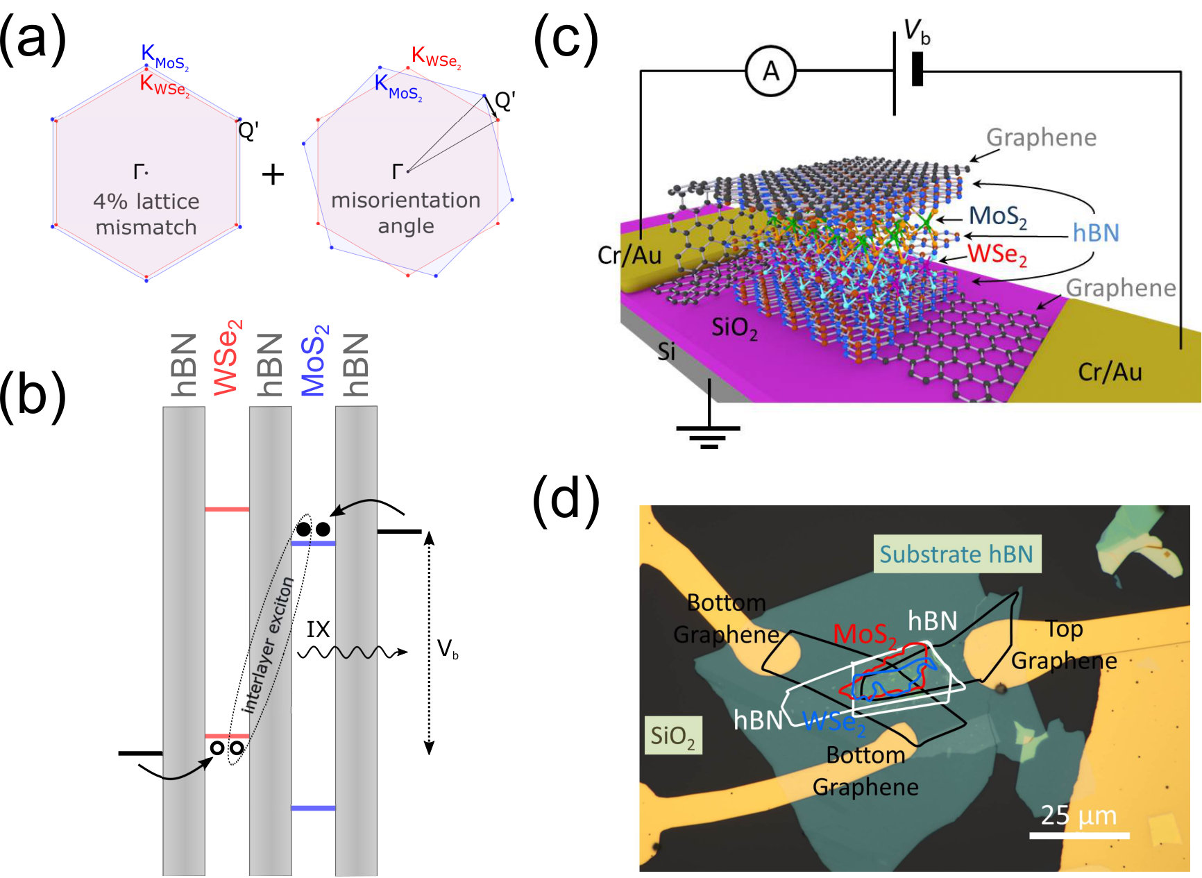 Figure 1
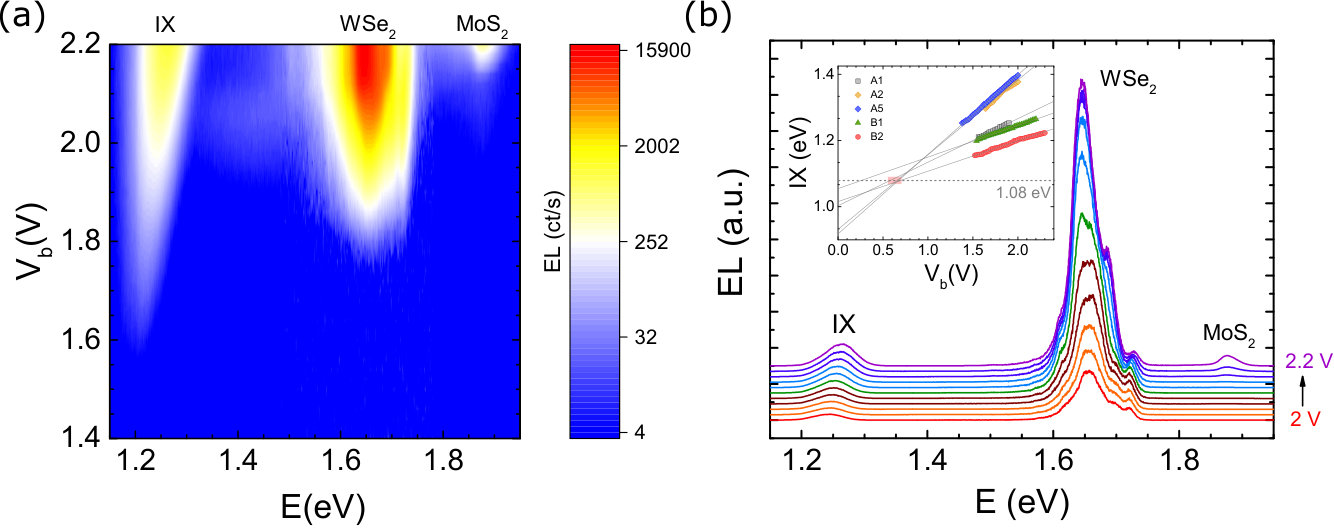 Figure 2
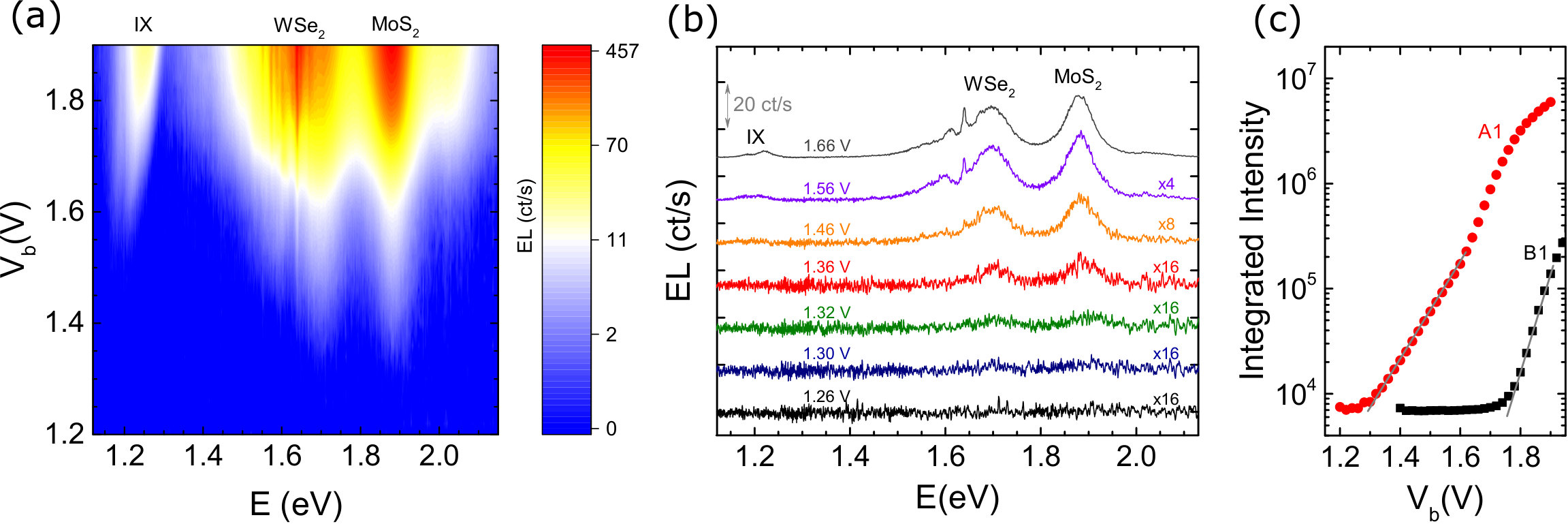 Figure 3
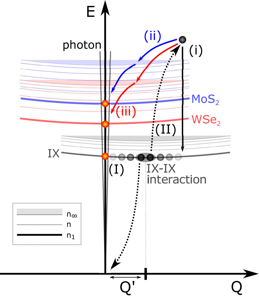 Figure 4
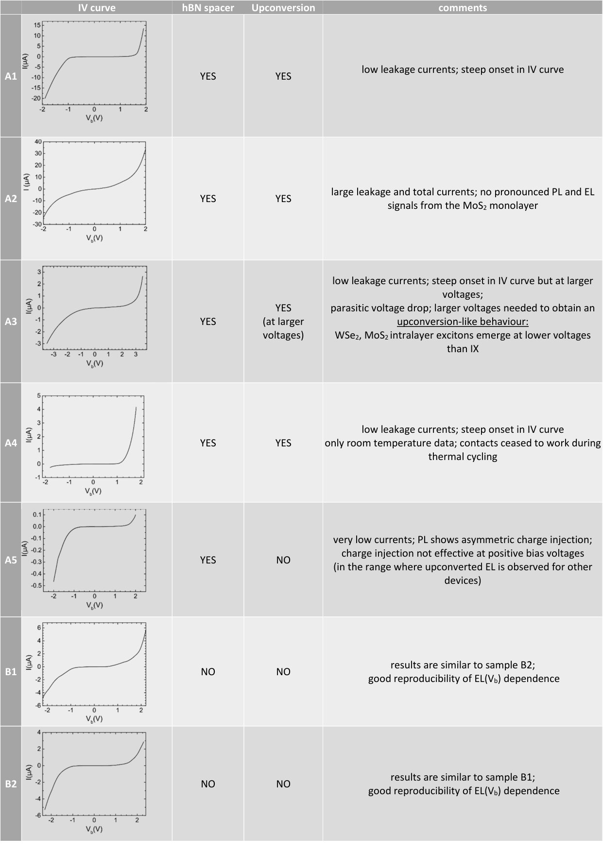 Figure 5
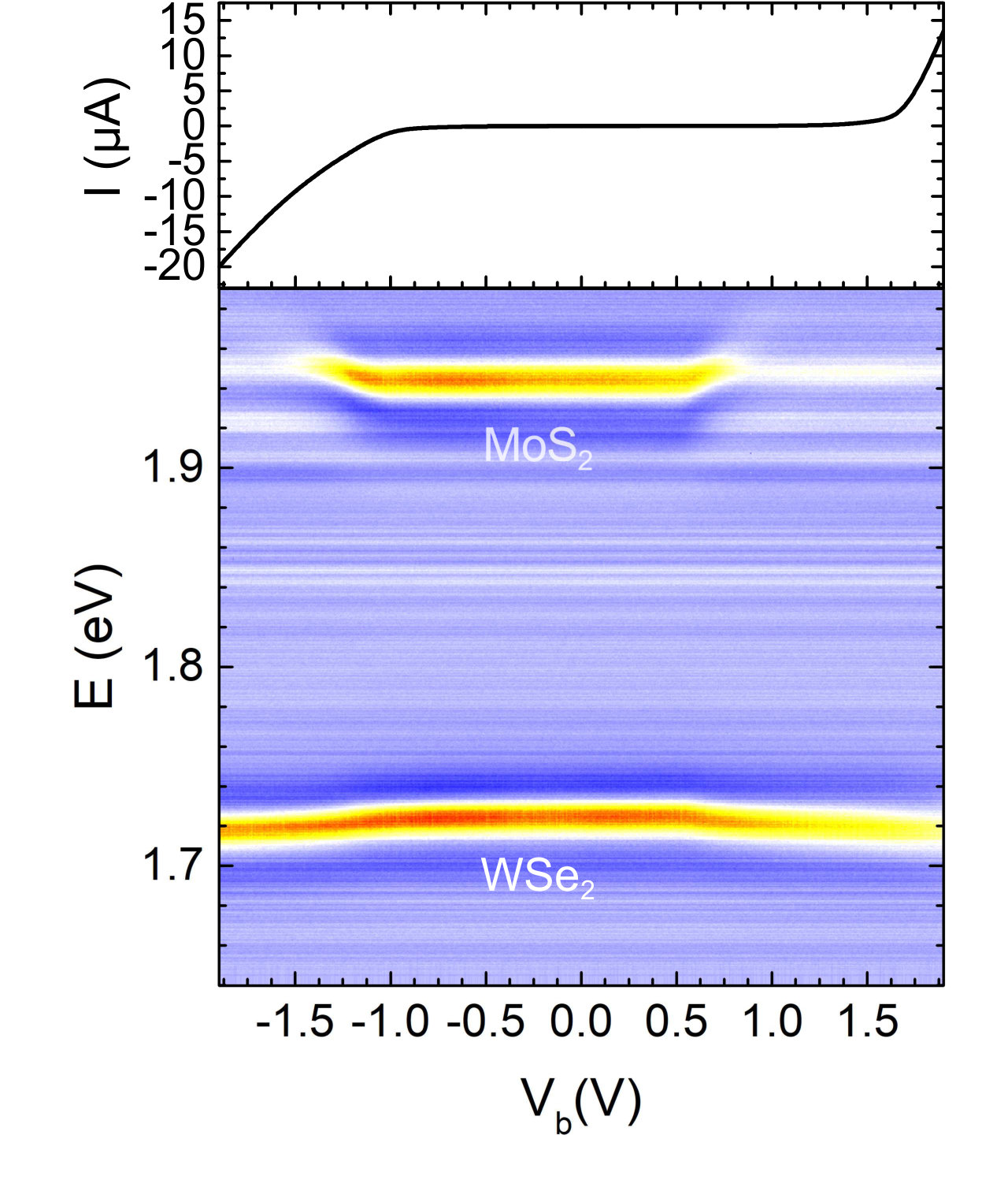 Figure 6
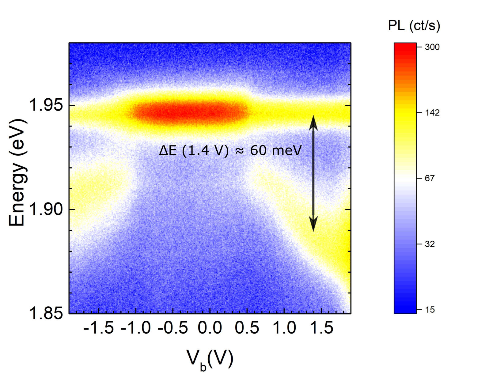 Figure 7
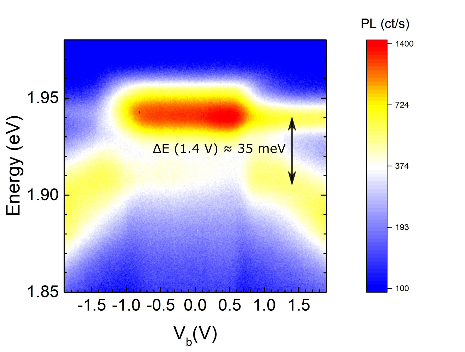 Figure 8
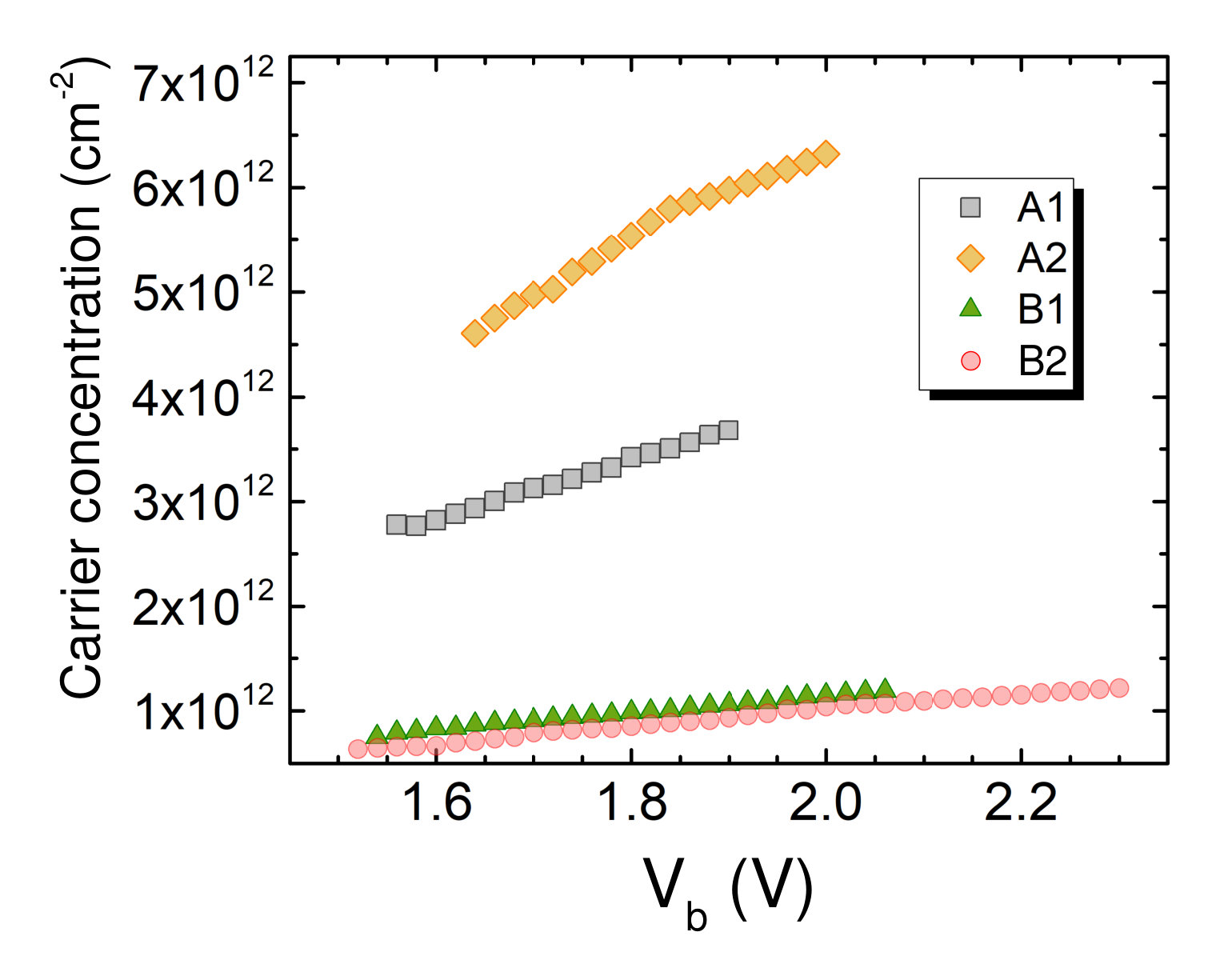 Figure 9
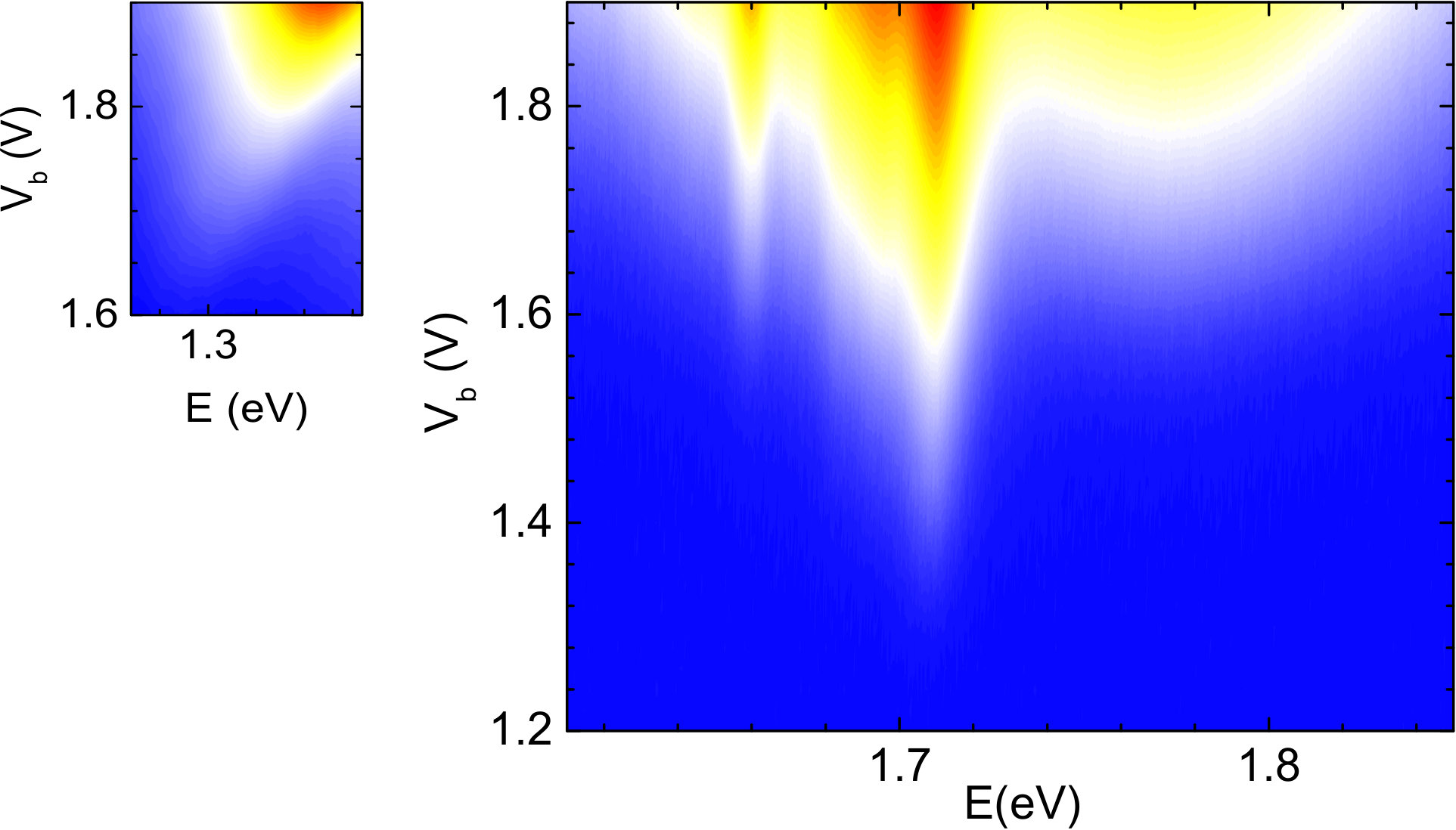 Figure 10
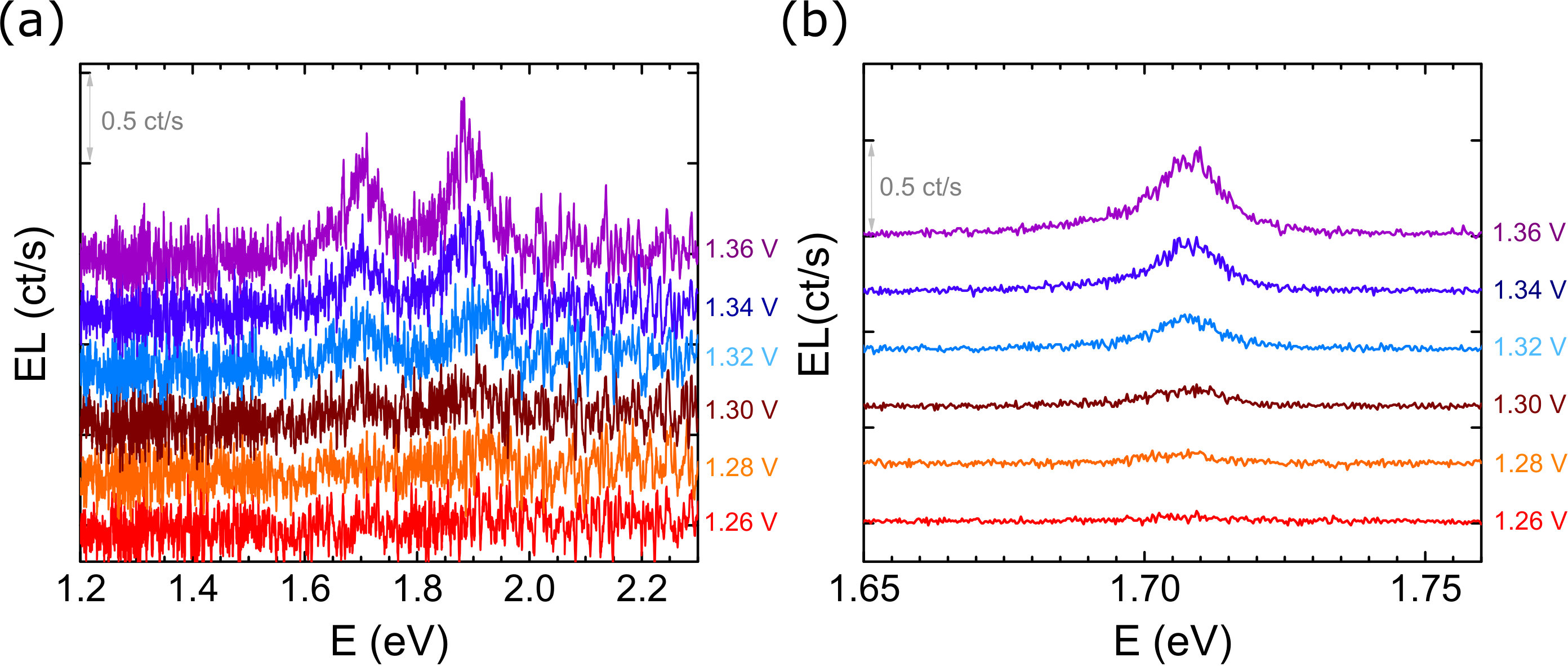 Figure 11
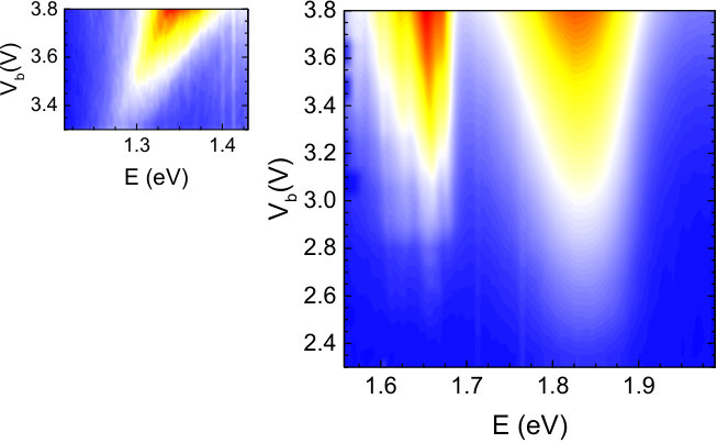 Figure 12
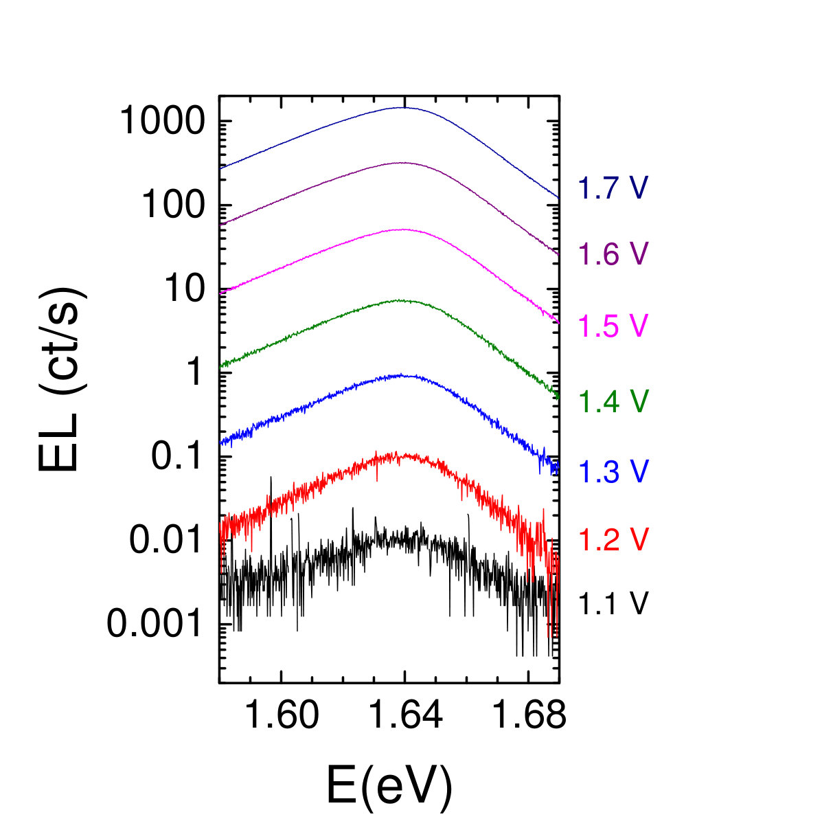 Figure 13
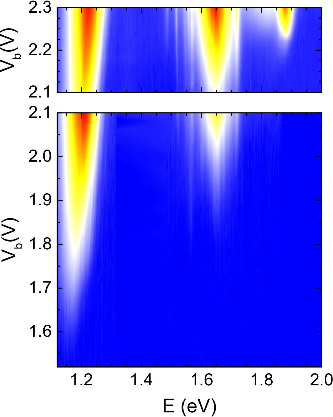 Figure 14
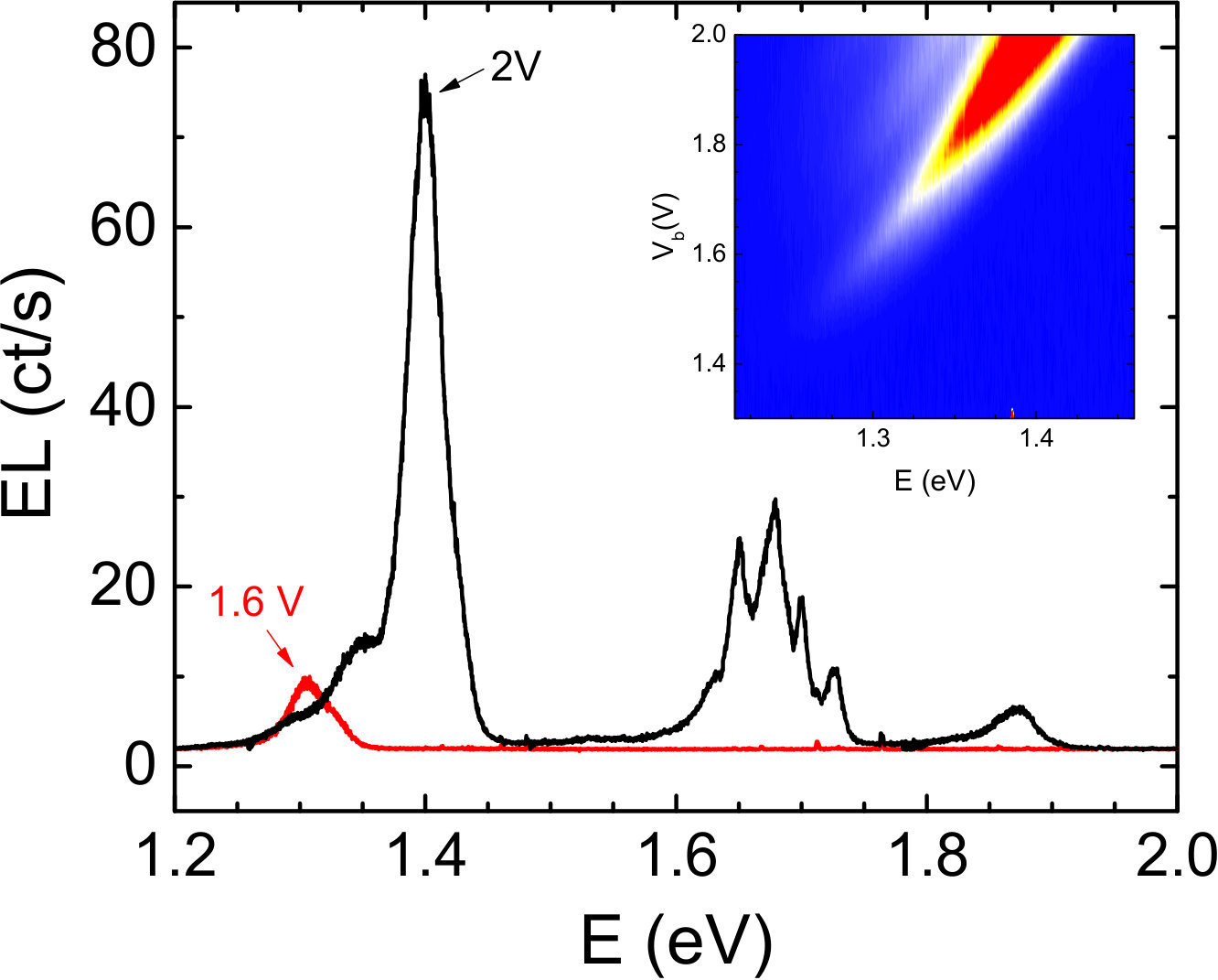 Figure 15
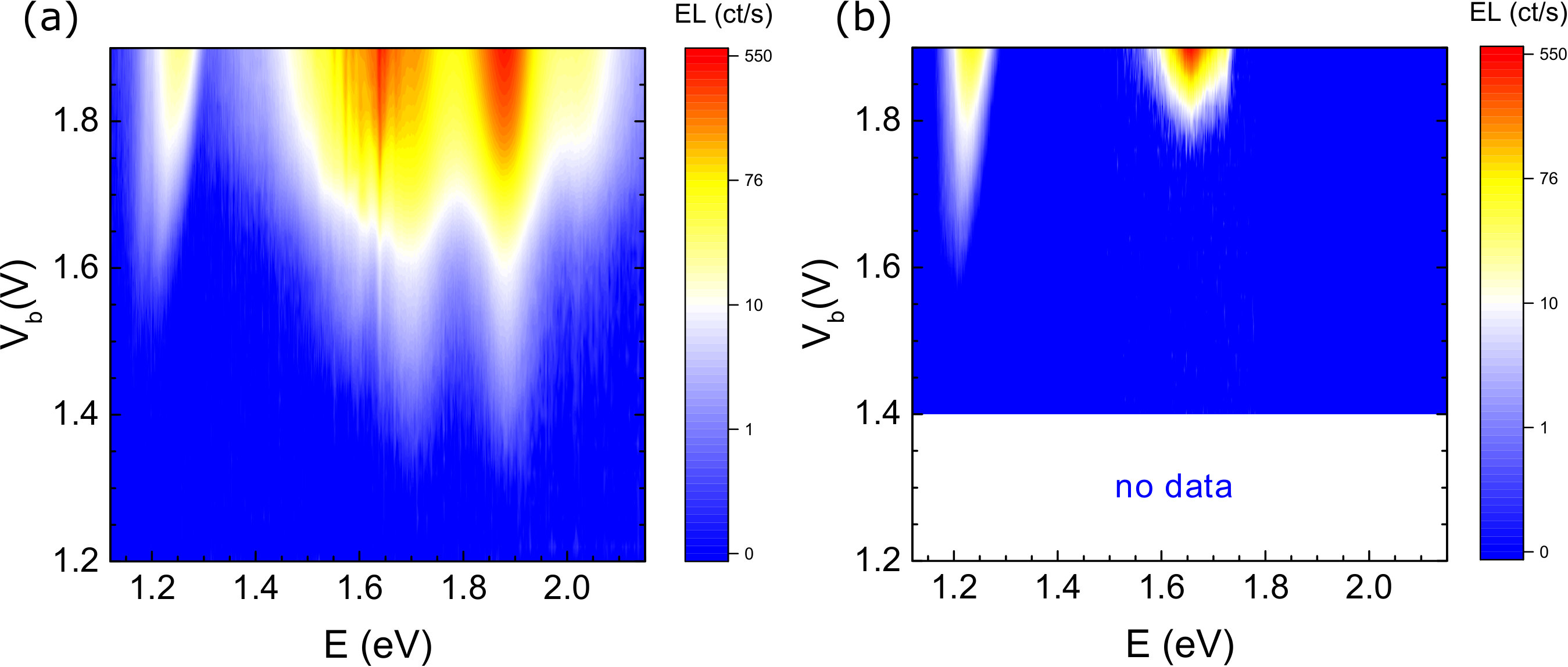 Figure 16
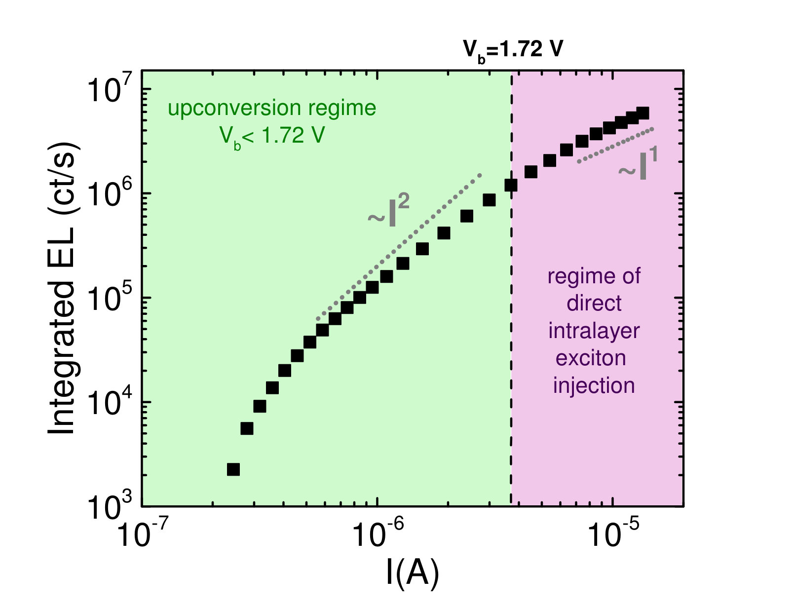 Figure 17
Peer Reviews
No public reviews on file for this paper yet. If you reviewed it on a platform where reviews are public (OpenReview, ICLR, NeurIPS, ICML), you can paste yours below so the community can read it here.
Videos
No videos yet. Explain this paper in a talk, walkthrough, or lecture? Add one.
††thanks: corresponding author††thanks: corresponding author
Upconverted electroluminescence via Auger scattering of interlayer excitons in van der Waals heterostructures
J. Binder
Laboratoire National des Champs Magnetiques Intenses, CNRS-UGA-UPS-INSA-EMFL, 25 Rue des Martyrs, 38042 Grenoble, France
Faculty of Physics, University of Warsaw, ul. Pasteura 5, 02-093 Warsaw, Poland
J. Howarth
School of Physics and Astronomy, University of Manchester, Oxford Road, Manchester M13 9PL, UK
National Graphene Institute, University of Manchester, Oxford Road, Manchester, M13 9PL, UK
F. Withers
Centre for Graphene Science, College of Engineering, Mathematics and Physical Sciences, University of Exeter, Exeter EX4 4QF, UK
M. R. Molas
Laboratoire National des Champs Magnetiques Intenses, CNRS-UGA-UPS-INSA-EMFL, 25 Rue des Martyrs, 38042 Grenoble, France
Faculty of Physics, University of Warsaw, ul. Pasteura 5, 02-093 Warsaw, Poland
T. Taniguchi
K. Watanabe
National Institute for Materials Science, 1-1 Namiki, Tsukuba 305-0044, Japan
C. Faugeras
Laboratoire National des Champs Magnetiques Intenses, CNRS-UGA-UPS-INSA-EMFL, 25 Rue des Martyrs, 38042 Grenoble, France
A. Wysmolek
Faculty of Physics, University of Warsaw, ul. Pasteura 5, 02-093 Warsaw, Poland
M. Danovich
School of Physics and Astronomy, University of Manchester, Oxford Road, Manchester M13 9PL, UK
National Graphene Institute, University of Manchester, Oxford Road, Manchester, M13 9PL, UK
V. I. Fal’ko
School of Physics and Astronomy, University of Manchester, Oxford Road, Manchester M13 9PL, UK
National Graphene Institute, University of Manchester, Oxford Road, Manchester, M13 9PL, UK
Henry Royce Institute for Advanced Materials, M13 9PL, Manchester, UK
A. K. Geim
K. S. Novoselov
School of Physics and Astronomy, University of Manchester, Oxford Road, Manchester M13 9PL, UK
National Graphene Institute, University of Manchester, Oxford Road, Manchester, M13 9PL, UK
M. Potemski
Laboratoire National des Champs Magnetiques Intenses, CNRS-UGA-UPS-INSA-EMFL, 25 Rue des Martyrs, 38042 Grenoble, France
Faculty of Physics, University of Warsaw, ul. Pasteura 5, 02-093 Warsaw, Poland
A. Kozikov
School of Physics and Astronomy, University of Manchester, Oxford Road, Manchester M13 9PL, UK
National Graphene Institute, University of Manchester, Oxford Road, Manchester, M13 9PL, UK
Abstract
The intriguing physics of carrier-carrier interactions, which likewise affect the operation of light emitting devices, stimulate the research on semiconductor structures at high densities of excited carriers, a limit reachable at large pumping rates or in systems with long-lived electron-hole pairs. By electrically injecting carriers into WSe2/MoS2 type-II heterostructures which are indirect in real and k-space, we establish a large population of typical optically silent interlayer excitons. Here, we reveal their emission spectra and show that the emission energy is tunable by an applied electric field. When the population is further increased by suppressing the radiative recombination rate with the introduction of an hBN spacer between WSe2 and MoS2, Auger-type and exciton-exciton annihilation processes become important. These processes are traced by the observation of an up-converted emission demonstrating that excitons gaining energy in non-radiative Auger processes can be recovered and recombine radiatively.
Introduction
Type-II heterostructures made of semiconducting monolayer transition metal dichalcogenides (TMDs) are excellent systems to study indirect interlayer excitons and their properties, in particular at high charge carrier densities. In the regime of large carrier injection many phenomena and processes become important that are negligible at low injection rates Pandey2007 ; Qian2010 ; He2016 . One of those processes is Auger recombination, a non-radiative decay of non-equilibrium carriers, inherent to any semiconducting material. Since for the Auger process to proceed at least three charge carriers are required, the process gains importance with increasing carrier densities. Notably, Auger-type processes become also a factor in limiting the performance of light-emitting diodes (LEDs) at high output powerIveland2013 . The importance of Auger-type exciton-exciton scattering processes was evidenced for direct intralayer excitons in semiconducting TMD monolayers by optical pump probe and time-resolved photoluminescence experiments Sun2014 ; Yuan2015 ; Poellmann2015 ; Yu2016 ; Aivazian2017 ; Kulig2018 . Here, we study indirect interlayer excitons in electroluminescent devices with a particular focus on the high carrier density regime.
In this work we employ constant electric carrier injection, which is the common operating condition for LEDs, to study the Auger recombination and exciton-exciton interactions. For this approach, without strong pumping, one has to render the radiative recombination inefficient to achieve large charge carrier densities. To this end we chose to study van der Waals (vdW) heterostructures with MoS2/WSe2, which are stable semiconducting TMDs that feature a type-II band alignment and a large lattice mismatch (), see Figure 1 (a) and (b). Such heterostructures allow us to study long-lived interlayer excitons (IX) in the energy range of eV, important for silicon photonics and telecommunication, with an emission wavelength that can be tuned by an applied electric field. To even further suppress the radiative recombination across the indirect bandgap we produced devices with a monolayer hBN spacer between the TMDs. In such devices the Auger processes are strongly enhanced, dominating the exciton dynamics. Comparison of the behavior of samples with different spacers allows us to establish the qualitative characteristics of exciton-exciton interaction. Besides Auger processes, there is additional interest in the regime of high carrier densities motivated by recent progress in TMD based excitonic devices Unuchek2018 and theoretical predictions that vdW heterostructures could allow observing effects like the condensation of excitons Wu2015 or high-temperature super-fluidity Fogler2014 .
Another ingredient besides the reduction of radiative recombination needed to establish large IX populations is the possibility to selectively inject electrons only into one and holes only into the other material. We met this prerequisite by using tunneling injection through graphene electrodes in vertical heterostructures. In contrary to optical injection Rivera2015 ; Rivera2016 ; Nagler2017 ; Miller2017 ; Zhu2017 ; Kunstmann2018 ; Unuchek2018 , for which electrons and holes are almost exclusively created in the same and not in different materials, the electrical injection scheme circumvents the competing short-lived direct intralayer recombination, since no charge carriers of different type are present in the same material. The injection process is illustrated in Figure 1 (b) and electroluminescence (EL) becomes the method of choice to characterize the devices. Strikingly, besides the observation of the EL of the IX, we observe a large upconversion effect enabling intralayer emission of WSe2 and MoS2 at voltages well below the voltages corresponding to the respective excitonic bandgaps.
Results
Van der Waals heterostructures for interlayer excitons
A schematic drawing of a typical device is presented in Figure 1 (c). Si/SiO2 is used as the substrate for the vdW heterostructure with the following layer sequence: Gr / 3-5 hBN / 1 WSe2 / 0-1 hBN / 1 MoS2/ 3-5 hBN / Gr. For all devices discussed in the text the outer hBN barriers were three to five layers thick. The middle thin hBN spacer was either one layer thick or completely absent. Based on the presence of this hBN spacer we can divide the devices studied into two groups: with and without a monolayer hBN spacer separating the TMDs. Our study comprised seven devices out of which five were fabricated with and two without a monolayer hBN spacer. The devices with hBN spacer are numbered A1 - A5 and samples without hBN spacer B1, B2. For all these devices the two TMDs were aligned under the optical microscope (estimated accuracy ). An optical microscope image of such a sample is shown in Figure 1 (d). Details about the device fabrication and the basic optical properties can be found in ref. Withers2015, and in the methods section. Figure 1 (b) illustrates the type-II band alignment of a WSe2/MoS2 vdW heterostructure with a monolayer hBN spacer and the tunneling pathways for charge carriers upon application of a voltage between the top and bottom graphene electrodes. The reported values for the band offsets of monolayer WSe2 and MoS2 are in the range of eV Kang2013 ; Gong2013 ; Ponomarev2018 for the conduction band offset, between eV Kang2013 ; Gong2013 ; Chiu2015 for the valence band offset and in the range of eV Kang2013 ; Gong2013 ; Ponomarev2018 for the interlayer bandgap. For the case depicted in the sketch, the voltage is large enough to enable electron injection into the MoS2 conduction band and hole injection into the WSe2 valence band (V V), but the voltage is below the threshold for direct WSe2 and MoS2 electron-hole injection (V V and V, respectively) Binder2017 . This selective injection of a given carrier type into only one material together with the large band offsets results in an extremely large charge build up at the interface and hence facilitates large IX populations.
Tunable electroluminescence of interlayer excitons
First, we discuss the experimental results typical for the devices (B1 and B2) without hBN spacer between the TMDs. Figure 2 (a) shows the evolution of the EL as a function of bias voltage in a broad energy range for sample B1. The EL spectra, Figure 2 (b), show three contributions: an emission originating from MoS2 at around 1.9 eV, a broad band at 1.7 eV related to WSe2 and a third peak at around 1.2-1.3 eV, which we attribute to IX emission. We can pinpoint this peak to originate from IX since we observe a strong blueshift as a function of bias voltage. This blueshift is a consequence of the electric field that builds up in our vertical tunneling structure upon applying the bias voltage, which results in an increase of the distance between the conduction band edge of MoS2 and the valence band edge of WSe2 (see Figure 1 (b)). This behavior was universal for all devices studied showing linear shifts with slopes in the range of 90-200 meV/V (see Figure 2 (b)). The different slopes are the result of the different effective thicknesses of the barriers. The shift of the IX is a measure of the electric field and can be used to estimate the IX density (see Supplementary Note 4). To determine the total IX shift one has to estimate the energy of a presumptive IX without electrically injected carriers. To this end, photoluminescence and reflectance contrast measurements (see Supplementary Note 4) were used to extract the threshold voltages for carrier injection (red shaded area in Figure 2 (b)). The extrapolation of the linear fits to this voltage yields an energy of about 1.08 eV for a presumptive IX without electrically injected carriers, in good agreement with an interface bandgap of 1.08 eV, recently extracted from transport measurements Ponomarev2018 . The IX emission energy in vertical vdW heterostructures is easily tunable, which is an interesting feature for many prospective applications. In contrast, no significant shift of the intralayer transitions as a function of bias voltage can be observed, in agreement with the fact that transitions in the same material are not sensitive to relative band movements caused by the electric field.
For both devices without an hBN spacer (results for device B2 are shown in Supplementary Note 3) the different contributions emerge one after another with increasing bias voltage. The IX emission appears first (V V), as the difference between the conduction band of MoS2 and the valence band of WSe2 constitutes the lowest barrier for electron-hole injection (see Figure 1 (b)). At larger voltages (V V) the WSe2 emission emerges, which is a result of tunneling into the intralayer excitonic states. Finally, at (V V) MoS2 emission becomes observable in accordance to the larger band-gap. It is interesting to note that the voltages for which EL can be observed correspond to the exciton emission energy rather than to the single particle band gap in agreement to what has been observed for vdW heterostructures with a single WSe2 monolayer Binder2017 .
Upconverted emission of intralayer excitons
The situation is different for the devices with a monolayer hBN spacer for which one expects a further reduced radiative recombination. The results are exemplary shown for device A1 in Figure 3 (a) (data for other devices is presented in Supplementary Note 2). Strikingly, one observes emission from both MoS2 and WSe2 at bias voltages as low as 1.3 V. The emitted photons at that voltage have an energy of around 1.7 eV (WSe2) and 1.9 eV (MoS2), which constitutes a remarkable upconversion of 0.6 eV. These measurements reveal electrically driven upconversion for light-emitting devices based on vdW heterostructures.
An additional interesting observation is that the onset of emission is virtually the same for both MoS2 and WSe2. Moreover, we note that the emission from WSe2 and MoS2 emerges at lower applied bias voltages than the emission from the IX in contrast to samples without an hBN spacer (compare to Figure 2 (a)). The EL spectra presented in Figure 3 (b) also clearly show that for the sample with an hBN spacer the contribution of the intralayer excitonic emission of WSe2 and MoS2 is much stronger than the IX emission. These major observations allow drawing the following important conclusions. First, the process seems not to be dependent on the upconversion energy, since it shows equal onsets and intensities for both WSe2 and MoS2. Second, the upconversion process must be almost equally probable for electrons and holes, since in order to observe these intralayer excitons one has to lift holes into the valence band of MoS2 and electrons into the conduction band of WSe2 (compare Figure 1 (b)). Third, although the IX has a lower emission energy of 1.2-1.3 eV compared to around 1.9 eV (1.7 eV) for the intralayer excitons of MoS2 (WSe2), these intralayer excitons emerge at lower applied bias voltages in the EL spectra. Energetic upconversion was reported in literature for different inorganic semiconducting Jones2015 ; Manca2017 ; Seidel1994 ; Baumgartner2008 ; Potemski1991 as well as organic Pandey2007 ; Qian2010 ; He2016 materials. In the case of upconversion beyond the energy-scale of phonons commonly Auger-processes were identified to be responsible for the effects. The observation of substantially different onset voltages for measurable intralayer emission in samples A1 and B1 is highlighted in Figure 3 (c) (see also Supplementary Figure 8). Clearly, the intralayer emission appears in our spectra at bias voltages as low as V V for sample A1, whereas this emission becomes visible at larger voltages V V in sample B1. One must however note that the definition of these onset voltages is somewhat arbitrary, defined by the actual experimental conditions/sensitivity (the background signal). As discussed below and illustrated in Figure 3 (c), one should not expect a complete disappearance of Auger processes in sample B1, but their efficiency being orders of magnitude smaller in sample B1 as compared to sample A1.
Auger processes and upconversion mechanism
Thanks to the purely electrical carrier injection in our devices we can rule out nonlinear effects involving photon absorption. It is therefore intuitive to investigate whether Auger processes can account for the above described observations. Such an Auger process would proceed in the following manner: (i) An electron in MoS2 and a hole in WSe2 form an IX that recombines non-radiatively. (ii) The excess energy is transferred to another electron in the MoS2 conduction band. (iii) Since the transferred energy is larger than the band offset the electron can tunnel into the WSe2 conduction band. (iv) Due to the large number of holes present in the valence band of WSe2, the electron can form a WSe2 intralayer exciton and recombine radiatively, which gives rise to the characteristic light emission for WSe2 monolayers. A similar process would be possible for holes in the valence band of WSe2. With such a process one can account for the energy independence of the process, which is true as long as the energy of the indirect transition is larger than the band offsets. However, the second aspect identified above, i.e. same probability for the upconversion of electrons and holes, is hard to imagine in such a case. For such an Auger process to be efficient there should be a state to which the charge carrier can be excited. Yet in the case of WSe2 there are no bands with an energy distance of the order of the IX energy in the band structure around the K point to which a hole could be excited Danovich2016 . Even if one includes larger momenta it is hard to imagine that such a process would be equally probable as compared to electrons for which such bands should be present. In this picture it is also difficult to explain why upconversion sets in at lower bias voltages than the IX emission. In order to overcome this conceptual discrepancies, we propose an excitonic Auger process instead of the above described single particle considerations in agreement with the exciton-exciton interactions observed in optical pump-probe experiments Sun2014 ; Poellmann2015 ; Yu2016 ; Aivazian2017 ; Kulig2018 .
Figure 4 presents the proposed mechanism responsible for the upconverted EL in the two-particle picture. The grey (red, blue) solid parabola represents the exciton dispersion of the IX (WSe2, MoS2). The dashed lines represent exited states and the shaded filled area stands for the excitonic continuum. Due to the lattice mismatch, the parabola describing the IX is shifted towards higher momenta. If there is an additional misalignment angle this will further increase the distance Q’ (see Figure 1 (a)). As a result of the effective selective injection of carriers the population of IX increases. The distribution function of the population is schematically depicted by the shading of the grey circles. The orange circles stand for excitons that possess almost zero center of mass velocity and hence can recombine radiatively (light cones).
In this picture, the IX have to compensate for the additional momentum Q’ first in order to recombine radiatively. This can be achieved in two ways: (I) by increasing the IX population at larger voltages. Since with increasing bias electrons and holes that form the IX possess larger and larger momenta, a significant amount of the IX population will as well extend more and more towards larger momenta. The momentum range of efficient radiative recombination is determined by the photon dispersion, as indicated in Figure 4. If their momentum roughly equals Q’, the IX can recombine radiatively. Otherwise, the IX remains optically silent and gives rise to an increasing population that enables mechanism (II) through IX-IX collisions. As a result, one IX recombines non-radiatively and transfers the energy and momentum to a second IX (dotted arrows in Figure 4). This IX is excited into the continuum of excitonic states and has now three different decay channels: (i) the IX relaxes back into the IX ground state. This scenario is also called exciton-exciton annihilation. (ii) corresponds to the case where the now almost delocalized exciton relaxes into a state that corresponds to the MoS2 intralayer exciton. Please note that the relaxation process shown here is indirect in real space, i.e. that in the single particle picture this would correspond to a tunneling of the electron into the MoS2 conduction band. Similarly possible is (iii) for which the excited exciton relaxes to a WSe2 exciton state. For both (ii) and (iii), the relaxation continues via intralayer excitonic states until the exciton reaches the bottom of the dispersion relation, where it can recombine radiatively.
Within this picture we can imagine (ii) and (iii) to be equally probable, since there is a plethora of excited excitonic states for both materials, in contrast to the lack of higher energetic hole bands around the K point in the single particle picture. One can also explain the lower voltages for the onset of upconversion compared to the onset for the IX emission. In order to recombine radiatively the IX have to compensate for the momentum Q’ (I), but below this threshold there is already a significant population of optically silent IX present that can give rise to the upconversion (II). This difference in onsets should strongly depend on the misorientation angle that adds to the momentum Q’ due to lattice mismatch. Based on literature values for the effective masses and lattice parameters Kormanyos2015 and by using an estimation of the momentum mismatch of for zero misalignment and for misalignment Yu2015 we can estimate the additional kinetic energy needed to recombine radiatively to be meV and meV, respectively. These energies indicate that such an emission could be temperature activated, but depends sensitively on the misalignment angle. It has been shown theoretically that for such structures one should expect six light cones irrespective of the layer misalignment angle, which are situated at a non-zero center of mass velocity Yu2015 . Consequently, the IX have to posses a large kinetic momentum or have to be scattered by defects or phonons into the light cones to recombine radiatively. Otherwise these IX remain dark as shown in Figure 4. This fact renders the observation of PL of the IX very ineffective Zhu2017 ; Kunstmann2018 ; Ponomarev2018 , but on the other hand offers an ideal platform to study many-body interactions allowing more easily reaching the large IX population regime. In the more widely studied system of MoSe2/WSe2 the lattice mismatch is small () which makes the PL of IX observable allowing to study the properties of the IX more directly Rivera2015 ; Rivera2016 ; Ross2017 ; Nagler2017 ; Miller2017 , but consequently not allowing for large IX populations. For our samples measured at low temperatures no PL of the IX could be observed in agreement with other recent reports Zhu2017 ; Kunstmann2018 ; Ponomarev2018 even with additional applied voltages. Please note that we only consider interlayer excitons where the electron and hole stem from the K points of the respective TMD layers. Recently, interlayer excitons were observed and identified in the photoluminescence of MoS2/WSe2 vdW heterostructuresKunstmann2018 . These interlayer excitons appear at larger energies of about 1.6 eV, which agrees with other reports of interlayer excitons in this material system Fang2014 ; Chiu2014 ; Unuchek2018 . In this work we were able to reveal the emission spectra of interlayer excitons which are not observable in PL. This observation is enabled thanks to our selective electrical injection mechanism, leading to large IX populations.
Discussion
Out of the seven devices studied, three showed upconverted EL emission. An additional device showed similar behavior – e.g. intralayer emission before IX – but at larger voltages suggesting that not the whole applied voltage dropped across the active region of the vdW heterostructure (see more detailed information on every device in Supplementary Note 1). All of these devices feature a monolayer hBN spacer. The two devices without hBN spacer did not show upconversion, as well as one sample with hBN spacer for which, however, charge injection was low and asymmetric. In our picture, we can also account for the behavior of the devices that do not show upconversion. Here, the consecutive appearance of different contributions with increasing bias voltage (compare Figure 2 (a)) is reflected by the increasing energetic positions of bright excitons around zero momentum (see Figure 4) into which the charge carriers can tunnel directly at larger voltages.
Our results suggest that the probability for Auger processes and upconversion versus radiative IX recombination can be effectively tuned by changing the thickness of the middle hBN barrier. The presence of an hBN spacer between the TMDs strongly influences the radiative recombination rate for IX emission in the vicinity of the light cone. By introducing an hBN spacer we increase the distance between the electron and the hole and consequently decrease the wave-function overlap. We can therefore expect the radiative recombination rate to be quenched in the case of devices from group A. Indeed, we observe that the upconverted intralayer emission is more intense than the IX emission (see Figure 3). Devices with an hBN spacer hence favor larger IX densities, since the radiative IX recombination at almost zero momentum becomes less effective.
To experimentally confirm this conjecture we estimated the IX density with two different methods: (i) by analyzing the apparent evolution of the exciton versus trion resonances in the MoS2 layer in photoluminescence (PL) and reflectance contrast (RC) measured as a function of bias voltage and (ii) by applying a simple capacitor model to account for the observed blueshift of the IX peak in the EL measured as a function of applied bias voltage, thus deducing the built-in electron-hole charge. Both methods (see Supplementary Note 4 for details on measurements and analysis) yield IX densities in the range of cm*-2* for sample A1, but distinctly smaller densities, in the range of cm*-2*, for sample B1. With these findings we indeed confirm our expectations that a larger accumulation of interlayer excitons appears in samples with an hBN spacer, favoring the observation of Auger processes in such structures.
However, the presence or absence (strong or weak efficiency) of the Auger processes should also be discussed with respect to an apparent ratio da of the inter exciton distance d to the exciton Bohr radius a. With n cm*-2* for sample A1 and n cm*-2* for sample B1 (see Supplementary Note 4) we obtain d nm and d nm, respectively for samples A1 and B1. To estimate a we note that the Bohr radius of an interlayer exciton is expected to be about a factor of two larger than that of the intralayer exciton Latini2017 . The exciton Bohr radius for intralayer excitons of semiconducting monolayer TMDs is known to be sensitive to the dielectric surrounding and varies in the range of 1 - 1.7 nm Wang2018 ; Stier2018 . Thus, given their hBN encapsulation, we roughly estimate a nm for the interlayer exciton Bohr radius in our structures and conclude that da for sample A1 and a significantly larger value da for sample B1. The conditions met by sample A1 are close to the Mott transition for interlayer excitons, which enables the observation of many body effects in this case Wang2018 . In addition, one may speculate that da can be further reduced in sample A1, as the introduction of an hBN spacer could lead to the reduction of the binding energy of the intralayer exciton in sample A1, as compared to sample B1. However, this reduction was calculated to be rather small Latini2017 , thus charge accumulation seems to be a decisive factor for the observation of the Auger-type processes in our samples.
An expected super-linear (ideally quadratic) behavior of the intensity of the Auger upconverted emission as a function of the IX density is another issue to be considered. It is tempting to trace this behavior by investigating the dependence of the emission intensity versus driving current. However, this dependence may also be super-linear due to trivial effects not related to the Auger process, like leakage currents due to device imperfections or exciton trapping centers, which are also observed in III-V quantum well structures Combescot2017 . For most of our devices we obtain an overestimation of the super-linear behavior of emission intensity as a function of driving current, due to current contributions that are not related to the emission process. Instead, for device A1, showing excellent I-V characteristics, the extracted super-linear trend in the regime of the Auger upconverted emission appears reliable, since in the case of this device the trend becomes practically linear in the direct intralayer injection regime, when the applied voltages exceed the excitonic bandgaps of the TMD monolayers (see Supplementary Figure 9). It is clear that more work on the role and nature of defects and a better control of the interfaces in vdW heterostructures is needed to tackle this issue for all devices.
In conclusion, we studied Auger processes in especially chosen type-II vdW heterostructures that enable large populations of optically silent IX. The double indirect nature of these excitons allows recovering a part of the excited Auger carriers through relaxation in optically active states. These states lie higher in energy than the initial IX, which results in the emission of upconverted photons. The large IX populations established thanks to the purely electrical tunnel injection allowed us to observe EL of otherwise silent IX, which shifts due to the electric field. It is shown that the IX energy can be tuned by up to 200 meV/V. A purely excitonic Auger process is proposed that, in contrary to Auger processes based on the single-particle picture, accounts for the major characteristics of the EL as a function of bias voltage. The results suggest that the efficiency of the upconversion mechanism depends on the hBN layer between the active TMDs. The revealed variable nature of the IX-IX interactions is of key importance for future TMD based optoelectronic device engineering and is important for any attempt aiming towards exciton condensation or super-fluidity in such structures.
Methods
Device Fabrication
All devices were fabricated on doped silicon substrates covered with silicon oxide 90 nm thick. Top graphene flakes were exfoliated on a silicon substrate spin coated with PMGI (polymethylglutarimide) and PMMA (polymethyl methacrylate). After dissolving PMGI, PMMA membranes with graphene were used to pick up other flakes. MoS2 and WSe2 were exfoliated on a silicon oxide substrate (290 nm thick) spin coated with PPC (polypropylene carbonate). Thin boron nitride and bottom graphene were exfoliated on silicon oxide substrates 70 and 90 nm thick, respectively. In some devices, we used substrate hBN about 30 nm thick exfoliated on silica substrates 90 nm thick. Light-emitting diodes were assembled by picking TMDs and hBN flakes one after another with the top graphene flake and transferring the resulting stack on top of bottom graphene. The PMMA membrane was then dissolved in acetone. In some devices, the flakes were picked up by top graphene and peeled onto the substrate hBN. After the assembly, electron-beam lithography was used to define a mask for contacts followed by evaporation of Chromium/Gold (Cr/Au, 3/50nm).
Optoelectronic measurements
The optoelectronic measurements were performed using two different helium flow cryostats (Janis ST-500, Oxford Instruments MicrostatHires) and a helium bath cryostat. All the measurements shown in the main text were taken at liquid helium temperature. The signal was collected using a 0.5 m long spectrometer equipped with liquid nitrogen cooled charge-couple-device (CCD) camera. Electrical measurements were performed using a Keithley 2450 source-measure unit synchronized with the spectrometer. A diode type behavior was observed for all devices.
Data availability
The data supporting the findings of this work are available from the corresponding author upon reasonable request.
Acknowledgments
This work was supported by the EC-FET European Graphene Flagship (no.785219), the ATOMOPTO project (TEAM programme of the Foundation for Polish Science co-financed by the EU within the ERDFund), the European Research Council (Synergy Grant Hetero2D), the Royal Society (UK), the Royal Academy of Engineering (UK), the Engineering and Physical Sciences Research Council (UK) grants EP/N010345/1, EP/S019367/1, EP/P026850/1, the US Army Research Office (W911NF-16-1-0279), the Elemental Strategy Initiative conducted by the MEXT, Japan and the CREST (JPMJCR15F3), JST.
Author Contributions
J.B. carried out the optoelectronic measurements, analyzed and interpreted experimental data, participated in discussions, developed the model and wrote the draft of the manuscript. A.K. produced experimental devices, participated in the measurements, analyzed and interpreted experimental data, contributed to writing the manuscript, J.H. produced experimental devices and participated in the measurements, F.W. produced experimental devices, M. R. M. participated in the measurements, K.W. and T.T. grew high-quality hBN, C.F., A.W., M.D., V.I.F. and A.G. participated in discussions, K.S.N. and M.P. initiated the project, analyzed experimental data, participated in discussions, contributed to writing the manuscript.
Competing Interests
The authors declare no competing interests.
The reference list from the paper itself. Each links out to its DOI / PubMed record.
- 1(1) Pandey, A. K. & Nunzi, J.-M. Upconversion injection in rubrene/perylene-diimide-heterostructure electroluminescent diodes. Appl. Phys. Lett. 90 , 263508 (2007).
- 2(2) Qian, L. et al. Electroluminescence from light-emitting polymer/Zn O nanoparticle heterojunctions at sub-bandgap voltages. Nano Today 5 , 384–389 (2010).
- 3(3) He, S.-J., Wang, D.-K., Jiang, N., Tse, J. S. & Lu, Z.-H. Tunable excitonic processes at organic heterojunctions. Adv. Mater. 28 , 649–654 (2016).
- 4(4) Iveland, J., Martinelli, L., Peretti, J., Speck, J. S. & Weisbuch, C. Direct measurement of Auger electrons emitted from a semiconductor light-emitting diode under electrical injection: identification of the dominant mechanism for efficiency droop. Phys. Rev. Lett. 110 , 177406 (2013).
- 5(5) Sun, D. et al. Observation of rapid exciton–exciton annihilation in monolayer molybdenum disulfide. Nano Lett. 14 , 5625–5629 (2014).
- 6(6) Yuan, L. & Huang, L. Exciton dynamics and annihilation in WS 2 2D semiconductors. Nanoscale 7 , 7402–7408 (2015).
- 7(7) Pöllmann, C. et al. Resonant internal quantum transitions and femtosecond radiative decay of excitons in monolayer W Se 2 . Nat. Mat. 14 , 889 (2015).
- 8(8) Yu, Y. et al. Fundamental limits of exciton-exciton annihilation for light emission in transition metal dichalcogenide monolayers. Phys. Rev. B 93 , 201111 (2016).