Effects of Hexagonal Boron Nitride Encapsulation on the Electronic Structure of Few-layer MoS$_2$
Xu Han, Jiangxiazi Lin, Junwei Liu, Ning Wang, Ding Pan

TL;DR
This study combines theoretical and experimental Raman spectroscopy to show that hBN encapsulation affects the electronic structure of few-layer MoS$_2$, inducing strain and potentially altering its semiconducting properties.
Contribution
It reveals that hBN encapsulation can induce strain in MoS$_2$, affecting its electronic properties, which challenges the assumption that hBN is electronically inert.
Findings
hBN encapsulation causes shifts in Raman modes of MoS$_2$
Encapsulation induces tensile strain in MoS$_2$ layers
Strain may lead to K-Q crossover in conduction band
Abstract
The hexagonal boron nitride (hBN) encapsulation has been widely used in the electronics applications of 2D materials to improve device performance by protecting 2D materials against contamination and degradation. It is often assumed that hBN layers as a dielectric would not affect the electronic structure of encapsulated 2D materials. Here we studied few-layer MoS encapsulated in hBN flakes by using a combination of theoretical and experimental Raman spectroscopy. We found that after the encapsulation the out-of-plane A mode is upshifted, while the in-plane E mode is downshifted. The measured downshift of the E mode does not decrease with increasing the thickness of MoS, which can be attributed to tensile strains in bilayer and trilayer MoS caused by the typical experimental process of the hBN encapsulation. We estimated the strain magnitude and…
Click any figure to enlarge with its caption.
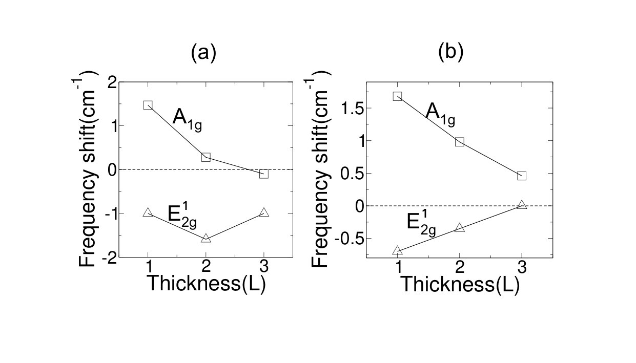 Figure 1
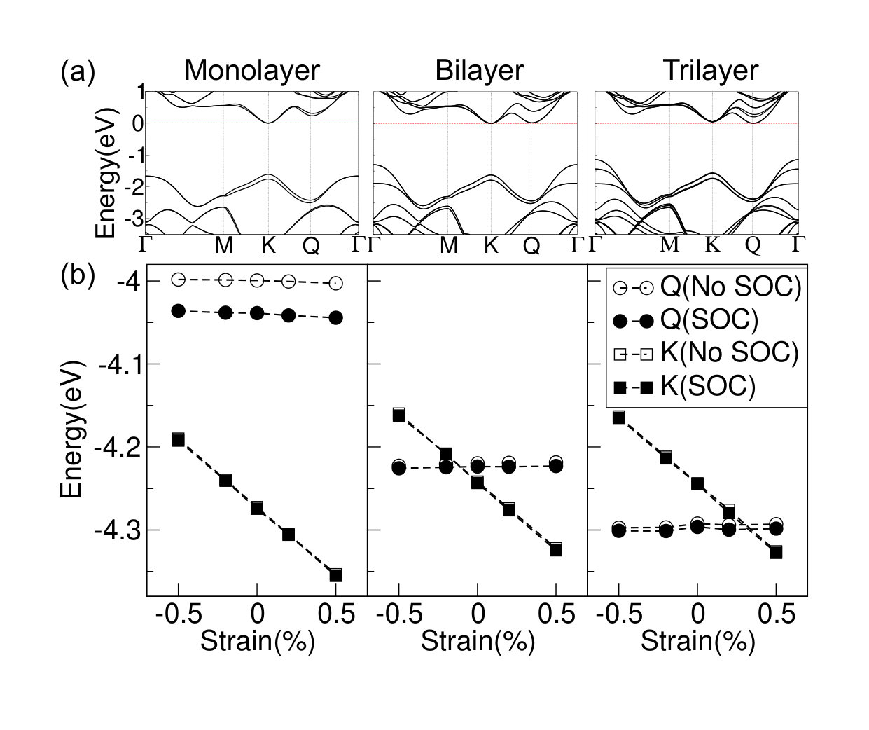 Figure 2
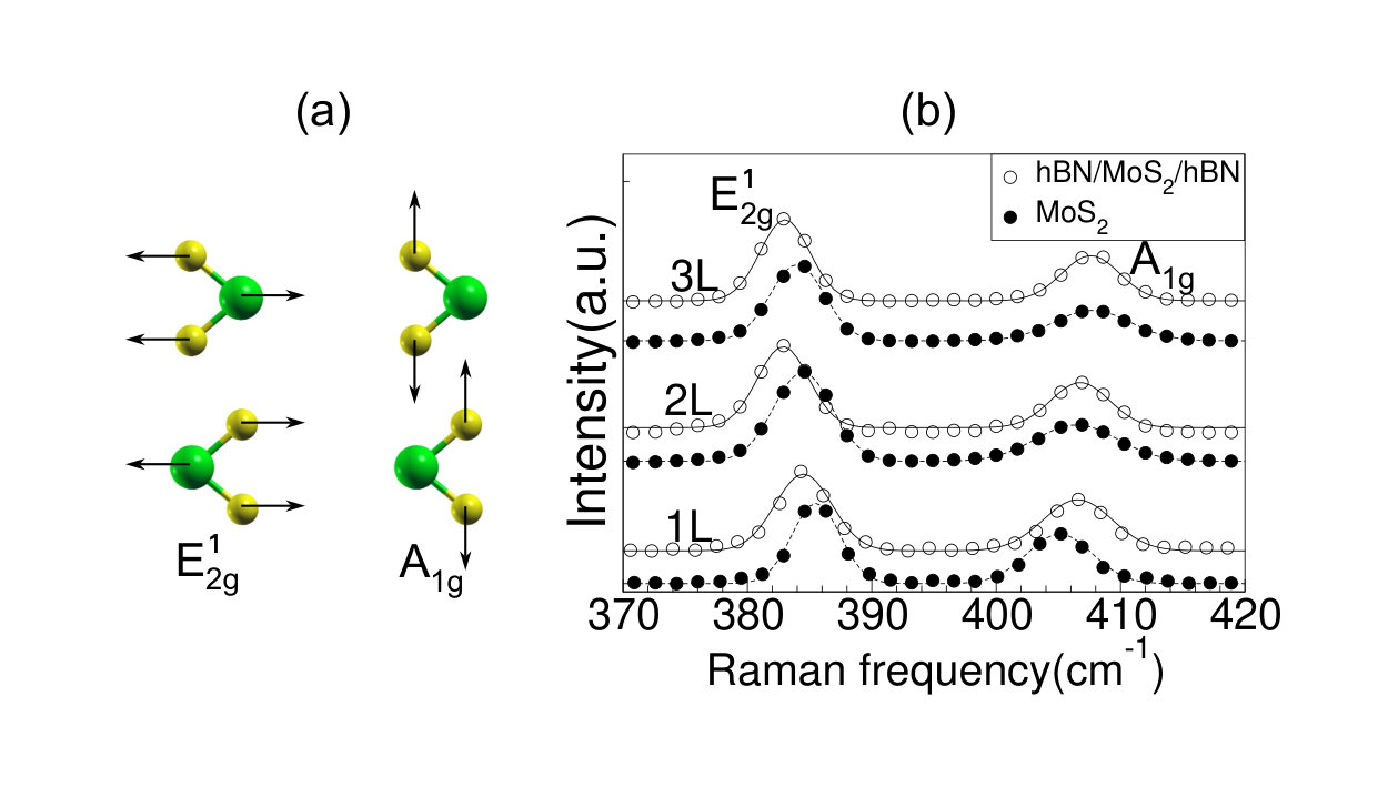 Figure 3
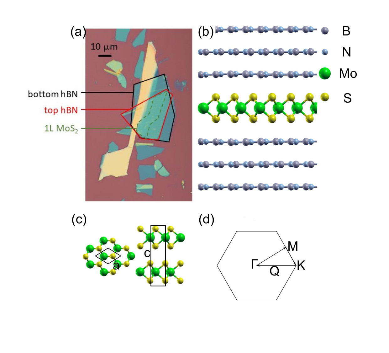 Figure 4
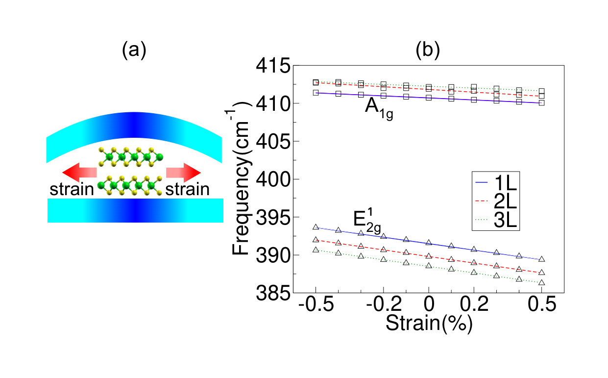 Figure 5
| 1L | 2L | 3L | |
|---|---|---|---|
| strain(%) | 0.06160.0005 | 0.28820.0015 | 0.22310.0015 |
Peer Reviews
No public reviews on file for this paper yet. If you reviewed it on a platform where reviews are public (OpenReview, ICLR, NeurIPS, ICML), you can paste yours below so the community can read it here.
Videos
No videos yet. Explain this paper in a talk, walkthrough, or lecture? Add one.
Effects of Hexagonal Boron Nitride Encapsulation on the Electronic Structure of Few-layer MoS2
Xu Han
Department of Physics, Hong Kong University of Science and Technology, Hong Kong, China
Jiangxiazi Lin
Department of Physics, Hong Kong University of Science and Technology, Hong Kong, China
Junwei Liu
Department of Physics, Hong Kong University of Science and Technology, Hong Kong, China
Ning Wang
Department of Physics, Hong Kong University of Science and Technology, Hong Kong, China
Ding Pan
Department of Physics, Hong Kong University of Science and Technology, Hong Kong, China
Abstract
The hexagonal boron nitride (hBN) encapsulation has been widely used in the electronics applications of 2D materials to improve device performance by protecting 2D materials against contamination and degradation. It is often assumed that hBN layers as a dielectric would not affect the electronic structure of encapsulated 2D materials. Here we studied few-layer MoS2 encapsulated in hBN flakes by using a combination of theoretical and experimental Raman spectroscopy. We found that after the encapsulation the out-of-plane A1g mode is upshifted, while the in-plane E mode is downshifted. The measured downshift of the E mode does not decrease with increasing the thickness of MoS2, which can be attributed to tensile strains in bilayer and trilayer MoS2 caused by the typical experimental process of the hBN encapsulation. We estimated the strain magnitude and found that the induced strain may cause the K-Q crossover in the conduction band of few-layer MoS2, so greatly modifies its electronic properties as an n-type semiconductor. Our study suggests that the hBN encapsulation should be used with caution, as it may affect the electronic properties of encapsulated few-layer 2D materials.
\altaffiliation
These authors contributed equally to this work.
\altaffiliationThese authors contributed equally to this work.
\alsoaffiliationDepartment of Chemistry, Hong Kong University of Science and Technology, Hong Kong, China
1 Introduction
Few-layer MoS2, a widely studied 2D material, has shown great potential for next-generation electronic devices 1, 2, 3. It can be made into an n-type 2, 3 or p-type 4 semiconductor with high carrier mobility, and the possible applications range from transistors 2 to water splitting electroncatalysts 5. Its electronic properties can be effectively tuned by the number of stacking layers as well as strain. Uniaxial, biaxial, and local strains have been applied, and many interesting phenomena were found 6, 7. For example, 2% uniaxial strain leads to a direct to indirect gap transition for monolayer MoS2 and 10% biaxial strain even converts it to a metal 8.
MoS2 thin films are found to be not stable in air, can be contaminated or oxidized at the surface, so in electronics applications, hexagonal boron nitride (hBN) layers are often used as a corrosion resistant coating to protect MoS2 9, 10. The hBN layers can be stable at more than 1000 ∘C in air and oxygen is unable to penetrate through even at high temperatures 11, 12. Moreover, the dangling-bond-free surface of hBN serves as an atomically flat substrate for MoS2, and when the hBN layers are put in between MoS2 and SiO2, they can screen the charge impurities in the SiO2 surface. Thus, the hBN encapsulation greatly improves carrier mobility and channel quality, so that quantum oscillations can be observed 9, 13. The hBN encapsulation is now widely used in device applications of many 2D materials, such as transition metal dichalcogenides 14, phosphorene 15, magic-angle graphene superlattices16.
From monolayer to bulk, the out-of-plane electronic dielectric constant of hBN, , increases from 2.89 to 3.03, while the in-plane changes little (4.964.98), according to the first-principles calculation 17. The band gap of hBN layers is between 5 and 6 eV 18, larger than that of few-layer MoS2. Thus, in 2D electronics applications, hBN layers often work as gate dielectrics for MoS2 9, 10, 18. In the previous studies about interactions between hBN and MoS2, hBN layers were usually treated as substrates, and have been shown to affect the optical properties of MoS2 due to the dielectric screening, such as photoluminescene emission 19, Raman 19, 20, and exciton 21 spectra. However, the effects of the hBN encapsulation on the electronic properties of MoS2 have not been well investigated. It is often assumed that the band structure and transport properties of MoS2 are not affected by the hBN encapsulation 9, 10.
Here, by a combination of theoretical and experimental methods, we studied the Raman spectra of few-layer MoS2 encapsulated in hBN flakes. We found that the typical experimental process of the hBN encapsulation may cause tensile strain in bilayer and trilayer MoS2, while the induced strain in monolayer MoS2 is negligible. The strain due to the hBN encapsulation may change the position of the conduction band minimum of few-layer MoS2, so greatly affects the transport properties of few-layer MoS2 as an n-type semiconductor.
2 Methods
2.1 Experimental methods
We used the well-developed dry transfer technique to stack the hBN/MoS2/hBN heterostructure 22. First, atomically-thin MoS2 flakes were exfoliated from bulk material onto a silicon wafer with a 280 nm SiO2 layer on top. A monolayer flake was identified using optical contrast. Raman spectroscopy was performed subsequently to this flake to confirm the number of MoS2 layers. Then we prepared two thin hBN flakes, one on another SiO2/Si wafer and the other one on a PMMA film. Using an optical microscope, the hBN layers on PMMA was aligned with the MoS2 flake by the natural cleavage edges of flakes and was used to separate MoS2 from the silicon wafer, then the obtained hBN/MoS2 stack was transferred onto the hBN on the SiO2/Si wafer. Finally, the PMMA film was removed by acetone. The encapsulated hBN/MoS2/hBN heterostructure was annealed at 300 ∘C in an argon protected environment for 6 hours to reduce organic residues and impurities. Raman spectroscopy was performed again to the same MoS2 flake now encapsulated by hBN. Experiments for bilayer and trilayer MoS2 followed the same procedures.
All Raman experiments were performed at ambient conditions using the InVia (Renishaw) micro Raman system with a 514.5 nm laser. The laser power was controlled at 0.15 mW and 2.5 mW for the exposed and encapsulated MoS2, respectively, to prevent damage to the sample.
2.2 DFT Calculations
Electronic structure calculations were performed using the plane-wave pseudopotential method implemented in the Quantum ESPRESSO package (version 6.1)23. The SG15 Optimized Norm-Conserving Vanderbilt (ONCV) pseudopotentials (version 1.1) were used24, 25. In the spin-orbital coupling (SOC) calculations, full relativistic pseudopotentials were from Ref 26. The kinetic energy cutoff for plane waves was 60 Ry. The convergence thresholds for energy, force, and stress were 10*-5* Ry, 10*-4* Ry/Bohr, and 50 MPa, respectively. We chose the local density approximation (LDA)27 as the exchange-correlation (xc) functional to calculate Raman frequencies (see below). For the band structure calculations, we used the PBE xc functional 28 with SOC. For multiple layers structures, the interlayer distances were obtained by the van der Waals functional optB88-vdW 29. A Monkhorst-Pack k-point mesh of 10101 was used with the primitive cells of few-layer MoS2 and 221 with the encapsulated MoS2. With periodic boundary conditions, the vacuum between two neighboring images is at least 12 Å.
The hBN/MoS2/hBN heterostructure was made by 55 hBN and 44 MoS2. We used three layers hBN to encapsulate MoS2 (see Fig. 1(b)). The in-plane lattice constant of the supercell was kept the same as that of free-standing MoS2, and we increased the in-plane lattice constant of hBN by 0.8% to fit the supercell.
Raman frequencies were calculated by using the frozen phonon method, where the atomic displacement was 0.05 bohr. Our phonon frequencies are in very good agreement with the results obtained by density functional perturbation theory 30. In the heterostructure calculations, we diagonalized the dynamic matrix at only:
[TABLE]
where is the phonon wave vector of MoS2, is the vibration frequency, and is the identity matrix.
3 Results and Discussion
Fig. 1(a) shows the topview of monolayer MoS2 encapsulated inside two hBN flakes, obtained by optical microscope. In Fig. 2, we compared the experimental Raman spectra of MoS2 encapsulated in hBN flakes and adsorbed on the SiO2/Si substrate. We increased the thickness of MoS2 from one to three layers to see the change of spectra. Two Raman modes, in-plane (E) and out-of-plane (A1g) as shown in Fig. 2(a), can be seen in the measured spectra in Fig. 2(b). For MoS2 adsorbed on SiO2/Si, with increasing the thickness of MoS2, the frequency of the A1g mode increases, while the E mode decreases (See Fig. S1(a)), so the frequency difference () between these two modes becomes larger. This is why the frequency difference can be used to count the number of MoS2 layers in experiment 31, and our finding is consistent with previous studies 31, 32. It has been reported that the stiffening of the out-of-plane mode A1g is attributed to the enhanced interlayer van der Waals (vdW) interactions 31, whereas the downshift of the in-plane mode E is mainly caused by the stronger dielectric screening of the long-range Coulomb interactions 32.
When the MoS2 layers are encapsulated in hBN flakes, the Raman peaks are shifted compared with those obtained from MoS2 on SiO2/Si, as shown in Fig. 3. The Raman frequency of the out-of-plane mode A1g becomes larger except for trilayer MoS2, while the frequency of the in-plane mode E decreases, so the frequency difference becomes larger after the encapsulation. As a result, when we use to count the number of MoS2 layers inside hBN flakes, caution is needed. For example, of monolayer MoS2 in hBN is even larger than that of bilayer MoS2 on SiO2/Si by 0.04 cm*-1*, as shown in Fig. S1 (c). The shift directions of the two modes caused by the hBN encapsulation are the same as the mode shift directions with increasing the thickness of MoS2, so for MoS2 held by hBN, the vdW interactions between MoS2 and hBN layers, and the dielectric screening due to the hBN layers also play important roles in modifying the A1g and E modes, respectively.
With increasing the thickness of MoS2 layers, the frequency shifts caused by the hBN encapsulation should become smaller, because the interface effects become less important and the vibration frequencies are getting close to those of bulk MoS2. In Fig. 3(a), however, the shift of the E mode does not decrease with the thickness of MoS2. Instead, bilayer MoS2 has the largest E mode shift. Unlike the E mode, the frequency shift of the A1g mode decreases with thickness, but in trilayer MoS2 it even decreases to a negative value: -0.1 cm*-1*.
To better understand the Raman frequency shifts caused by the hBN encapsulation, we performed density functional theory calculations (see methods). In Table SI, we compared four exchange-correlation(xc) functionals. The semilocal functional PBE 28 lacks vdW interactions, so it seriously overestimates the interlayer distance in bulk MoS2. When we applied the dispersion correction (PBE-D2)33 or used the vdW functional (optB88-vdW)29, the lattice constant of bulk MoS2 (see Fig. 1(c)) is improved considerably, but the vibration frequencies are still not as good as the ones obtained using the local density approximation (LDA)27. Due to the error cancellation, the LDA describes the interlayer interactions remarkably well, so here we used the LDA to compute Raman spectra of few-layer MoS2, as in many previous studies 32, 34.
The calculated frequency differences () between the modes A1g and E are given in Fig. S1(d). For MoS2 layers adsorbed on SiO2/Si and encapsulated by hBN, the frequency difference increases with increasing the number of layers, which is consistent with the experimental results in Fig. S1(c). In particular, for one to three MoS2 layers on SiO2/Si, the measured and calculated values differ within only 0.4 cm*-1*, indicating that our computational settings are very accurate to calculate vibration frequency differences for few-layer MoS2. The calculated frequency of the A1g mode of MoS2 in hBN is upshifted compared to that of MoS2 on SiO2/Si, while the E peak is downshifted, as show in Fig. 3(b). The shift directions are consistent with those found experimentally; however, the shift magnitudes are different. The experimental downshift of the E mode is larger than the calculated one, especially for bilayer and trilayer MoS2. In particular, the calculated downshift of the E mode decreases with increasing the thickness of MoS2 as expected, but the similar trend can not be found in the measured Raman spectra.
The inconsistency between the experimental and calculated Raman data suggests that some other factors may contribute to the measured Raman frequency shifts. Charge transfer and strain are two common reasons. Because hBN layers have a very low density of charge impurites, the charge transfer amount is negligible 19. Besides, Chakraborty et al. showed that charge transfer affects the A1g mode more than it does E 35, but in our measurements, the shifts of the A1g peak are less obvious than those of E. Thus, we can conclude that charge transfer does not play a major role in our experiments.
We consider the strain induced by the hBN encapsulation is biaxial. The biaxial strain is defined as , where and are the in-plane lattice constants with and without strain, respectively (see Fig. 1(c)). Fig. 4 shows the vibration frequencies of the A1g and E modes decrease with increasing the strain of few-layer MoS2. Apparently, the strain affects the E mode more than A1g, so the shift of the E mode can be used to evaluate the in-plane strain 36, 37. By polynomial fitting, we found that the frequency of the E mode has a linear relation with in the strain range in Fig. 4. For monolayer, bilayer, and trilayer MoS2, the mode changes by -4.23, -4.23, and -4.31 cm*-1* per 1 strain, respectively. From the difference between the measured and calculated downshifts of the E mode, we calculated the possible strains, which are 0.06, 0.29, and 0.22% for monolayer, bilayer, and trilayer MoS2, respectively (see Table I). The tensile strain also causes a tiny downshift of the A1g mode, so the A1g mode frequency of trilayer MoS2 even decreases by -0.1 cm -1 after the encapsulation, though the interlayer vdW forces stiffen the A1g mode.
It is interesting that bilayer and trilayer MoS2 have larger strains than monolayer MoS2. The lattice mismatch between hBN and MoS2 is as large as 21%, and the heterostructure layers are stacked together by vdW interactions, so the induced strain is not caused by the lattice mismatch. A possible reason is that a thicker MoS2 film might cause a larger deformation of hBN when we heated the heterostructure and pressed the top and bottom hBN layers very hard to squeeze out the air; the MoS2 layers were stretched and could not relax fully when held by the deformed hBN. We also measured the Raman spectra of the encapsulated bilayer MoS2 before annealing, and found that the biaxial strain is about 0.067%, much smaller than the strain after annealing, indicating that the experimental annealing process may induce a tensile strain.
Let us see how the electronic structure of MoS2 changes after being encapsulated by hBN. The band gap of hBN layers is between 5 and 6 eV, which is much larger than those of few-layer or bulk MoS2 indicating that the hBN layers are transparent for MoS2. In Fig. S2, we unfolded the band structure of the heterostructure supercell using the Brillouin zone of MoS238 and found that both the valance band top and the conduction band bottom of the heterostructure come from MoS2, so the semiconductor devices made by hBN/MoS2/hBN heterostructures only show the electronic properties of MoS2.
The strain induced by the hBN encapsulation affects the electronic properties of MoS2. Fig. 5 shows the band structures of few-layer MoS2 under strain. For bilayer and trilayer MoS2 in the biaxial strain between -0.5% and +0.5%, the valance band maximum (VBM) is always at the point, whose position moves up with respect to the vacuum level when increasing the biaxial strain. For conduction bands, with increasing the biaxial strain, the K valley position moves down with respect to the vacuum level, whereas the Q point does not change much (see Fig. 5). Particularly, for the trilayer MoS2, the conduction band minimum (CBM) changes from Q to K when the strain is 0.26%, which is comparable to the estimated strain caused by the hBN encapsulation. Thus, it is possible that when increasing the thickness of few-layer MoS2, the CBM should move from K to Q, but the tensile strain due to the hBN encapsulation changes it back to the K point.
Since the K and Q valley electrons are very different, the K-Q crossover changes conduction band properties significantly. In the first Brillouin zone of few-layer MoS2, the valley degeneracy of the K point is twofold, while that of the Q point is sixfold, so the densities of states at these two valley point are different, leading to different Landau level filling factors in quantum oscillation measurements 9, 13. Besides, the effective mass of the Q valley electrons is larger than that of the K valley electrons, as shown in Fig. S4. With increasing the biaxial strain, the effective mass at the Q point increases, while it decreases at the K point, so the hBN encapsulation may amplify the effective mass difference.
4 Conclusion
To summarize, we studied few-layer MoS2 encapsulated in hBN flakes by using a combination of density functional theory and experimental Raman spectroscopy. We found that after the encapsulation the out-of-plane A1g mode is upshifted due to the interlayer vdW interactions between hBN and MoS2, while the in-plane E mode is downshifted, which can be attributed to the dielectric screening of hBN. The measured downshift of the E mode does not decrease with increasing the thickness of MoS2, indicating that the typical experimental process of the hBN encapsulation may induce a tensile strain in bilayer and trilayer MoS2.
The strain due to the experimental process of the hBN encapsulation may cause the Q-K crossover in the conduction band of few-layer MoS2. The Q and K valley electrons have different degeneracy and effective masses, so the hBN encapsulation does not only provide a dielectric surrounding for MoS2, but may also substantially affect the transport properties of few-layer MoS2 as an n-type semiconductor.
The hBN encapsulation has been widely used in many 2D materials applications to improve the device performance and stability. The encapsulation process may also induce the similar tensile strain in those few-layer materials and affect their electronic properties. The combined theoretical and experimental approach introduced here can be used to estimate the magnitude of the strain and to check whether the hBN encapsulation would affect the desired properties of few-layer 2D materials. The induced strain may be also used to further tune the electronic properties of vdW heterostructure devices.
5 Acknowledgement
N. W. acknowledges support from Hong Kong Research Grants Council (Project No. GRF-16300717). J. L. acknowledges support from the Hong Kong Research Grants Council (Project No. ECS-26302118). D. P. acknowledges support from Hong Kong University of Science and Technology by the start-up grant and from the Croucher Foundation through the Croucher Innovation Grant.
{suppinfo}
- •
Table SI: Calculated lattice constants of bulk MoS2 and Raman frequencies of the E and A1g modes in monolayer MoS2.
- •
Figure S1: Calculated Raman spectra of few-layer MoS2 adsorbed on SiO2/Si and encapsulated in hBN flakes.
- •
Figure S2: Calculated band structure of monolayer MoS2 with and without the hBN encapsulation.
- •
Figure S3: Calculated band structure of few-layer MoS2 under strain.
- •
Figure S4: Calculated effective masses of the Q and K valley electrons in few-layer MoS2.
This information is available free of charge via the Internet at http://pubs.acs.org
The reference list from the paper itself. Each links out to its DOI / PubMed record.
- 1Splendiani et al. 2010 Splendiani, A.; Sun, L.; Zhang, Y.; Li, T.; Kim, J.; Chim, C.-Y.; Galli, G.; Wang, F. Emerging Photoluminescence in Monolayer Mo S 2 . Nano Letters 2010 , 10 , 1271–1275
- 2Radisavljevic et al. 2011 Radisavljevic, B.; Radenovic, A.; Brivio, J.; Giacometti, V.; Kis, A. Single-Layer Mo S 2 Transistors. Nature Nanotechnology 2011 , 6 , 147
- 3Ganatra and Zhang 2014 Ganatra, R.; Zhang, Q. Few-Layer Mo S 2 : A Promising Layered Semiconductor. ACS Nano 2014 , 8 , 4074–4099
- 4Zhan et al. 2012 Zhan, Y.; Liu, Z.; Najmaei, S.; Ajayan, P. M.; Lou, J. Large-Area Vapor-Phase Growth and Characterization of Mo S 2 Atomic Layers on a Si O 2 Substrate. Small 2012 , 8 , 966–971
- 5Wan et al. 2018 Wan, Y.; Zhang, Z.; Xu, X.; Zhang, Z.; Li, P.; Fang, X.; Zhang, K.; Yuan, K.; Liu, K.; Ran, G. et al. Engineering Active Edge Sites of Fractal-Shaped Single-Layer Mo S 2 Catalysts for High-Efficiency Hydrogen Evolution. Nano Energy 2018 , 51 , 786–792
- 6Liang et al. 2017 Liang, J.; Zhang, J.; Li, Z.; Hong, H.; Wang, J.; Zhang, Z.; Zhou, X.; Qiao, R.; Xu, J.; Gao, P. et al. Monitoring Local Strain Vector in Atomic-Layered Mo Se 2 by Second-Harmonic Generation. Nano Letters 2017 , 17 , 7539–7543
- 7Yun et al. 2012 Yun, W. S.; Han, S. W.; Hong, S. C.; Kim, I. G.; Lee, J. D. Thickness and Strain Effects on Electronic Structures of Transition Metal Dichalcogenides: 2H- M X 2 𝑀 subscript 𝑋 2 {MX}_{2} Semiconductors ( M 𝑀 {M} = = Mo, W; X 𝑋 {X} = = S, Se, Te). Physics Review B 2012 , 85 , 033305
- 8Li 2012 Li, T. Ideal Strength and Phonon Instability in Single-Layer Mo S 2 . Physical Review B 2012 , 85 , 235407