Impact of intrinsic and extrinsic imperfections on the electronic and optical properties of MoS2
J. Klein, A. Kerelsky, M. Lorke, M. Florian, F. Sigger, J. Kiemle, M., C. Reuter, T. Taniguchi, K. Watanabe, J. J. Finley, A. Pasupathy, A. W., Holleitner, F. M. Ross, and U. Wurstbauer

TL;DR
This study investigates how different substrates and intrinsic defects influence the electronic and optical properties of monolayer MoS2, revealing substrate-dependent variations in doping, defect passivation, and exciton binding energy.
Contribution
It provides a detailed analysis of substrate effects and defect passivation in MoS2, improving understanding of how to optimize 2D material properties for quantum nanosystems.
Findings
SiO2 induces high doping and band tail states
hBN substrates reduce defect impact and doping
Quasiparticle gap matches optical spectra with 480 meV exciton binding energy
Abstract
Intrinsic and extrinsic disorder from lattice imperfections, substrate and environment has a strong effect on the local electronic structure and hence the optical properties of atomically thin transition metal dichalcogenides that are determined by strong Coulomb interaction. Here, we examine the role of the substrate material and intrinsic defects in monolayer MoS2 crystals on SiO2 and hBN substrates using a combination of scanning tunneling spectroscopy, scanning tunneling microscopy, optical absorbance, and low-temperature photoluminescence measurements. We find that the different substrates significantly impact the optical properties and the local density of states near the conduction band edge observed in tunneling spectra. While the SiO2 substrates induce a large background doping with electrons and a substantial amount of band tail states near the conduction band edge of MoS2,…
Click any figure to enlarge with its caption.
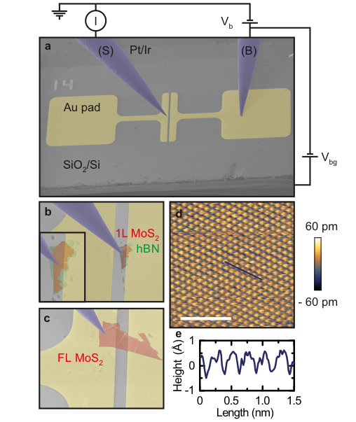 Figure 1
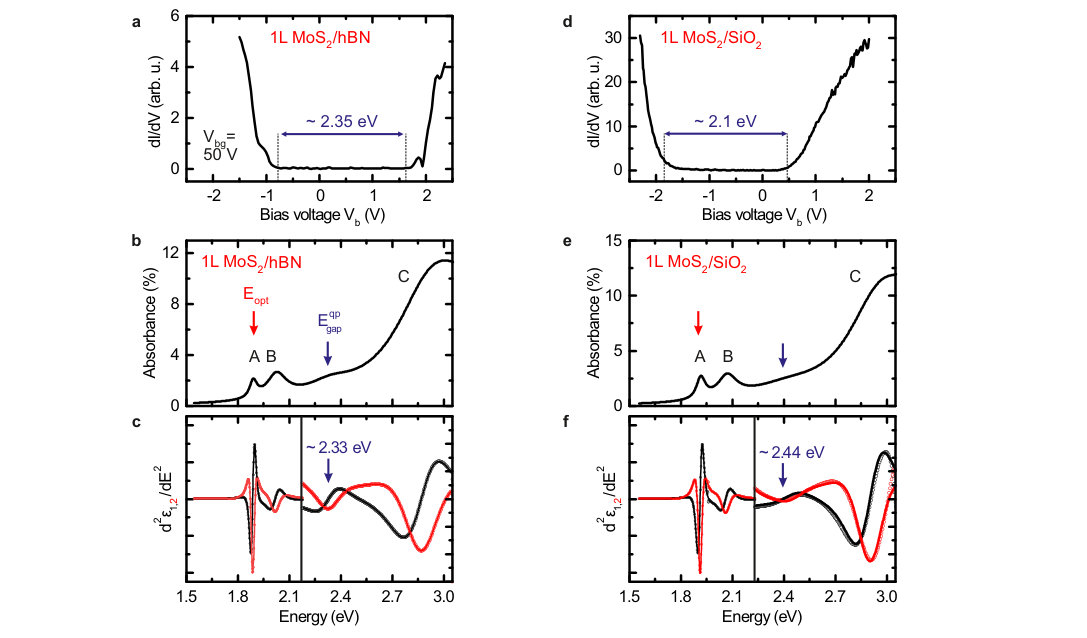 Figure 2
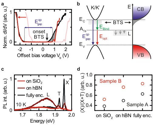 Figure 3
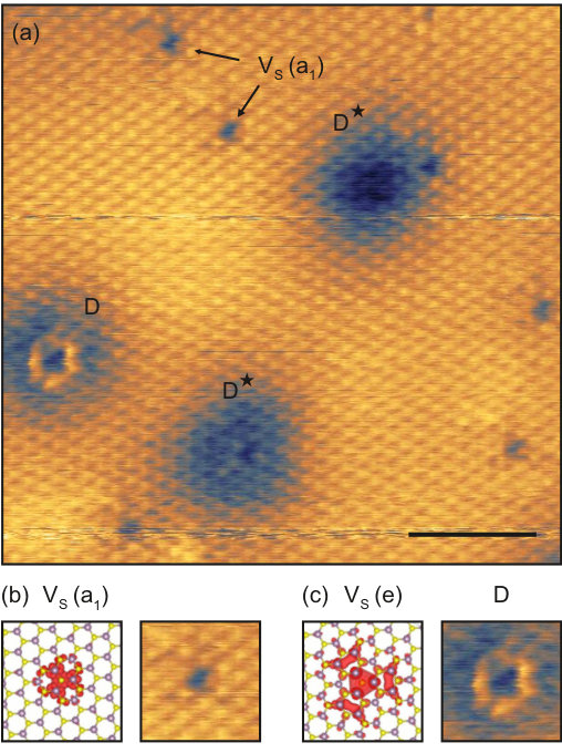 Figure 4
Peer Reviews
No public reviews on file for this paper yet. If you reviewed it on a platform where reviews are public (OpenReview, ICLR, NeurIPS, ICML), you can paste yours below so the community can read it here.
Videos
No videos yet. Explain this paper in a talk, walkthrough, or lecture? Add one.
Taxonomy
TopicsChalcogenide Semiconductor Thin Films
\alsoaffiliation
Nanosystems Initiative Munich (NIM), 80799 Munich, Germany
\alsoaffiliationBremen Center for Computational Materials Science, University of Bremen, 28359 Bremen, Germany
\alsoaffiliationNanosystems Initiative Munich (NIM), 80799 Munich, Germany \alsoaffiliationMunich Center for Quantum Science and Technology (MCQST), 80799 Munich, Germany
\alsoaffiliationNanosystems Initiative Munich (NIM), 80799 Munich, Germany \alsoaffiliationMunich Center for Quantum Science and Technology (MCQST), 80799 Munich, Germany
\alsoaffiliationDepartment of Materials Science and Engineering, Massachusetts Institute of Technology, Cambridge, MA 02139, United States
\alsoaffiliationNanosystems Initiative Munich (NIM), 80799 Munich, Germany \alsoaffiliationInstitute of Physics, University of Münster, 48149 Münster, Germany
\AtBeginShipoutNext\AtBeginShipoutDiscard
Impact of intrinsic and extrinsic imperfections on the electronic and optical properties of MoS2
J. Klein
Walter Schottky Institut and Physik Department, Technische Universität München, 85748 Garching, Germany
A. Kerelsky
Department of Physics, Columbia University, New York, New York 10027, United States
M. Lorke
Institut für Theoretische Physik, Universität Bremen, 28334 Bremen, Germany
M. Florian
Institut für Theoretische Physik, Universität Bremen, 28334 Bremen, Germany
F. Sigger
Walter Schottky Institut and Physik Department, Technische Universität München, 85748 Garching, Germany
J. Kiemle
Walter Schottky Institut and Physik Department, Technische Universität München, 85748 Garching, Germany
M. C. Reuter
IBM T. J. Watson Research Center, Yorktown Heights, NY 10598, United States
T. Taniguchi
National Institute for Materials Science, Tsukuba, Ibaraki 305-0044, Japan
K. Watanabe
National Institute for Materials Science, Tsukuba, Ibaraki 305-0044, Japan
J. J. Finley
Walter Schottky Institut and Physik Department, Technische Universität München, 85748 Garching, Germany
A. Pasupathy
Department of Physics, Columbia University, New York, New York 10027, United States
A. W. Holleitner
Walter Schottky Institut and Physik Department, Technische Universität München, 85748 Garching, Germany
F. M. Ross
IBM T. J. Watson Research Center, Yorktown Height, NY 10598, United States
U. Wurstbauer
Walter Schottky Institut and Physik Department, Technische Universität München, 85748 Garching, Germany
Abstract
Intrinsic and extrinsic disorder from lattice imperfections, substrate and environment has a strong effect on the local electronic structure and hence the optical properties of atomically thin transition metal dichalcogenides that are determined by strong Coulomb interaction. Here, we examine the role of the substrate material and intrinsic defects in monolayer MoS2 crystals on SiO2 and hBN substrates using a combination of scanning tunneling spectroscopy, scanning tunneling microscopy, optical absorbance, and low-temperature photoluminescence measurements. We find that the different substrates significantly impact the optical properties and the local density of states near the conduction band edge observed in tunneling spectra. While the SiO2 substrates induce a large background doping with electrons and a substantial amount of band tail states near the conduction band edge of MoS2, such states as well as the high doping density are absent using high quality hBN substrates. By accounting for the substrate effects we obtain a quasiparticle gap that is in excellent agreement with optical absorbance spectra and we deduce an exciton binding energy of about 480 meV. We identify several intrinsic lattice defects that are ubiquitious in MoS2, but we find that on hBN substrates the impact of these defects appears to be passivated. We conclude that the choice of substrate controls both the effects of intrinsic defects and extrinsic disorder, and thus the electronic and optical properties of MoS2. The correlation of substrate induced disorder and defects on the electronic and optical properties of MoS2 contributes to an in-depth understanding of the role of the substrates on the performance of 2D materials and will help to further improve the properties of 2D materials based quantum nanosystems.
1 Introduction
The electronic structure of atomically thin transition metal dichalcogenides (TMDCs) is unique due to the weak non-local dielectric screening of the Coulomb interaction. 1 The large surface-to-volume ratio makes these materials highly sensitive to changes in the dielectric environment. This has been exploited as a tuning knob to control excitonic properties and quasiparticle gaps in these materials. 2, 3 Taking full advantage of TMDCs requires an understanding of the relationship between the electronic properties of the materials and their environment. This involves measuring key electronic and optical properties in the presence of both extrinsic effects from the surroundings and intrinsic, atomic scale defects. The electronic properties of TMDCs can be probed by various experimental methods. Angle-resolved photo emission spectroscopy (ARPES), scanning tunneling spectroscopy (STS), photoluminescence excitation (PLE) spectroscopy and optically probing Rydberg states allow the determination of the quasiparticle band gap E energy. 4, 5, 6, 7, 8, 9, 10, 11, 12, 13, 14 The values are typically compared to the onset energy Eopt in optical absorbance or photoluminescence spectra to obtain the excitonic binding energy Ebin = E - Eopt. Experimental 4, 5, 6, 7, 9, 10, 11, 12, 13, 14 and theoretical 15, 16, 17, 18, 19, 20, 3 values for the binding energy vary widely in the literature, even for similar device geometries. In general, scanning tunneling spectroscopy (STS) is the method of choice for obtaining the quasiparticle gap from tunneling spectra since it is a direct probe of the local density of states (LDOS). Scanning tunneling microscopy (STM) is a favourable tool for visualizing defects with sub- spatial resolution and determining their densities in mono- and few-layer TMDCs and other materials. 21, 22, 23, 24, 25, 26, 27, 28
Transition metal dichalcogenide (TMDC) crystals are often prepared by mechanical cleavage and then transferred onto SiO2 substrates that allow optical identification. However, SiO2 as a substrate is well-known to exhibit dangling bonds and near-surface charge traps and is therefore not the substrate of choice for applications that require good sample quality and homogeneity. 29, 30 In contrast, the use of hBN as a substrate in van der Waals heterostructures has been widely established since it significantly enhances the electronic and photo-physical properties of atomically thin TMDCs, greatly reducing inhomogeneous linewidth broadening in photoluminescence 31, 32, 33, 3 and enabling large carrier mobilities due to strongly reduced scattering in field effect devices. 34, 35
Here, we combine STS, optical absorbance and photoluminescence spectroscopy to investigate the impact of these two different substrates on the electronic and optical properties in monolayer MoS2. We complementary measure the structure and density of intrinsic atomic scale defects. We quantitatively compare STS spectra recorded on exfoliated MoS2 monolayers placed on SiO2 and hBN. Using SiO2 as substrate, we find significant contribution of band tail states (BTS) below the conduction band (CB) that obscure the determination of the quasiparticle gap E and in turn the extracted exciton binding energy Ebin. The BTS are absent when using hBN as a substrate. Moreover, the use of hBN reduces the electron density shifting the Fermi level further to the center of the band gap, making the TMDC crystal more intrinsic. We find that the n-type doping is, due to both the SiO2 substrate and intrinsic defects. The later most likely due to a large density of native sulfur vacancies that we determine from STM topography measurements and in agreement with previous reports. 25, 36, 37 Moreover, low-temperature photoluminescence spectroscopy on nominally identical samples and on fully hBN encapuslated MoS2 monolayers is performed to cross-correlate the influence of the substrate on the electronic and optical properties. Taking into accound the various spectroscopy methods applied to the different sample geometries we discuss that the impact of the environment and SiO2 substrates on the intrinsic lattice defects are passivated if an hBN substrate or encapsulation with hBN is used.
2 Results and discussion
The samples investigated throughout this manuscript are fabricated by mechanical exfoliation and deterministic transfer onto thermally grown SiO2/Si substrates or on few layer hBN flakes that are also supported by SiO2/Si. The MoS2 flakes are either contacted by direct transfer onto a thin Au/ Ti pad or by evaporation of Au/Ti with similar thicknesses through a shadow mask to exclude any surface contamination from residues of photo-resist. STM/STS measurements are taken at room temperature. The STM is equipped with multiple tips and a scanning electron microscope (SEM) that allows mono- and few-layer MoS2 samples and van der Waals heterostructures to be located and probed. 38
Figure 1a shows a false color SEM image of a typical sample. A bias is applied between the biasing (B) and the scanning (S) tip which are both made from PtIr and a bias between the bias tip and the degenerately doped Si substrate can be applied to gate the device. A close-up SEM image of a monolayer MoS2 on hBN van der Waals heterostack and a few-layer MoS2 sample is shown in Fig. 1b and c. A typical constant current topography map of few-layer MoS2 is shown in Fig. 1d revealing atomic resolution and the hexagonal lattice symmetry from the topmost sulfur layer. A corresponding line cut is shown in Fig. 1(e) yielding the expected S-S distance of . 39
We now turn to the measurement of the local density of electronic states (LDOS) from STS and of the quasiparticle gap that is extracted from the LDOS. STS spectra that are proportional to the LDOS are shown in Fig. 2a and d for monolayer MoS2 on hBN and SiO2 substrates, respectively. Vanishing values in the spectrum correspond to the absence of electronic states and allows the determination of an apparent gap in the LDOS. For ideal semiconducting materials, the onset of the for negative bias voltages can be assigned to the valence band edge (VB) and the onset for positive bias voltages the conduction band edge (CB). The position of the Fermi energy is at zero bias voltage.
We begin with discussing the STS of monolayer MoS2 stacked onto high quality hBN which is an atomically flat and charge neutral insulating 2D material. 35 The spectrum of monolayer MoS2 on hBN is shown in Fig. 2a. In order to record the curve a backgate voltage of 50\text{,}\mathrm{V} is used to reach sufficient conductivity. The STS measurement shows an apparent gap in the LDOS of $\sim$2.35\text{\,}\mathrm{eV} with both the CB and the VB exhibiting a steep increase in density of states. We perform optical absorbance spectroscopy on a nominally identical sample for direct comparison with the tunneling spectra. The optical absorbance spectrum is shown in Fig. 2b. The spectrum reveals absorption from the A and B exciton transition at and . Moreover, by performing a critical point analysis by converting the absorbance spectrum to the real and imaginary part of the dielectric function utilizing Kramers-Kronig constraint analysis 40 and taking the second derivative 41, 12 as shown in Fig. 2c, we determine a quasiparticle gap of 2.33\text{,}\mathrm{eV}, which is in excellent agreement with the LDOS gap obtained from tunneling spectra. Therefore, we assign the LDOS gap from STS to the quasiparticle gap $E^{qp}_{gap,STS}\sim$2.35\text{\,}\mathrm{eV}. From the emission of the 1s exciton (A exciton), we can directly determine the exciton binding energy through . Taking from tunneling (absorbance) spectra we obtain an exciton binding energy of 460\text{\,}\mathrm{meV}$~{}($440\text{\,}\mathrm{meV}$)$ in good agreement with theory that predicts values of $E_{Bind}=300-$700\text{\,}\mathrm{meV} 15, 16, 17, 18, 20, 3 and binding energies obtained from optical spectroscopy measurements reporting of 600\text{,}\mathrm{meV}$$. 7, 12
Similar to the measurement on the hBN substrate, we perform tunneling and optical spectroscopy on monolayer MoS2 on SiO2 substrate as shown in Fig. 2d and e, respectively. Here, the monolayer MoS2 on the normally used SiO2 substrate reveals an apparent gap in the LDOS of 2.1\text{,}\mathrm{eV}, a value that is in good agreement with values from STS measurements on monolayer MoS*2* on SiO*2* in literature. [4](#bib.bib4), [6](#bib.bib6), [9](#bib.bib9), [10](#bib.bib10), [11](#bib.bib11), [13](#bib.bib13) Intriguingly, we observe the onset of the quasiparticle gap from absorbance measurements in Fig. [2](#S2.F2)e and the related critical point analysis in Fig. [2](#S2.F2)f at an energy of $E^{qp}_{gap,Abs}\sim$2.44\text{\,}\mathrm{eV}, much higher than the value from the STS data. Determination of the binding energy from pure optical measurements shown in Fig. 2e reveals 530\text{,}\mathrm{meV}, taking into account the optical gap $E_{A}=$1.91\text{\,}\mathrm{eV}, in good agreement with theory and other optical measurements, but more than twice the binding energy using the apparent gap from STS measurements shown in Fig. 2d.
In TMDCs, the exciton binding energy directly depends on the surrounding dielectric environment. For the static case and in the limit of long wavelengths (), the dielectric constant of the environment is approximated by an average dielectric constant of the surrounding dielectrics. 42, 43 For air/vacuum)/MoS2/SiO2, we obtain an average dielectric constant of with . 44 For air(vacuum)/MoS2/hBN, we get with . 45 Considering these values, we expect an exciton binding energy that is slightly larger for air(vacuum)/MoS2/SiO2 compared to air(vacuum)/MoS2/hBN due to a weaker dielectric screening. The for air(vacuum)/MoS2/hBN is most likely to be overestimated due to an air gap between MoS2 and hBN of 5\text{,}\mathrm{\SIUnitSymbolAngstrom} [46](#bib.bib46) that lowers dielectric screening. [3](#bib.bib3) This explains why $E_{bin}$ is very similar in both dielectric environments as observed in the all optical absorbance measurements, but a few tens of $\text{\,}\mathrm{meV}$ larger for the MoS*2* monolayer on SiO*2* with $E_{bin}\sim$440\text{\,}\mathrm{meV} and 480\text{,}\mathrm{meV}$$ for the 1s exciton in MoS2 on hBN and SiO2, respectively. From similar considerations regarding the dielectric environment, we expect to obtain also very similar quasiparticle gaps for MoS2 on SiO2 and on hBN in agreement with the optical measurements but in disagreement with the apparent gap in the LDOS from STS measurements.
To further investigate the origin of this discrepancy, we directly compare the STS spectra for MoS2 monolayers on SiO2 and hBN. We make two main observations: First, it is evident that in addition to the larger STS gap, the Fermi level is shifted close to the middle of the apparent gap in the LDOS with hBN as substrate compared to SiO2. For MoS2 on SiO2, the apparent gap is smaller and the Fermi level is close to the conduction band edge, showing the commonly observed n-type behavior of MoS2. The origin of excess electrons is not yet fully understood, but has been tentatively attributed to defects in the crystal lattice 47 and charge traps in the SiO2 substrate. 29 Second, the rise of LDOS at the conduction band edge is much steeper for monolayers on hBN than on SiO2 (see Fig. 2a,d). The rise of the LDOS at the valence band edge is similar on both substrates. This is further visualized in Fig. 3a by overlapping the onset for negative bias voltages in the traces assigned to the valence band maxima by offsetting the curves to match the valence bands for MoS2 on both substrates. The LDOS clearly matches in the valence band tail but is strictly steeper at the onset, attributed to differences in the conduction band for MoS2 on hBN than on MoS2 on SiO2.
We attribute the additional and more slowly raising LDOS at the CB of MoS2 on SiO2 to the emergence of band tail states (BTS) due to the SiO2 substrate (see Fig. 3b). 30 The surface of SiO2 is subject to dangling bonds and near-surface charge traps 29 that can severely impact the electronic properties of TMDCs as observable in tunneling spectroscopy by the introduction of interfacial states between the SiO2 and the MoS2. In particular, silanol groups (Si-O-H) are expected at the SiO2 surface due to plasma treatment prior to the MoS2 transfer. 48 The silanol groups are negatively charged and are reported to exist in large densities of \text{,}{\mathrm{cm}}^{-2}$$. 48 Similarly, it has been reported for electronic devices prepared from CVD grown MoS2 on SiO2 that the electronic transport properties are severely limited by such band tail trapping states. 49 Earlier work also described the influence of surface charge traps on the transport properties of MoS2. 50. As a consequence of the existence of such substrate induced BTS, the onset of LDOS in STS measurements for positive bias voltages does not directly mark the conduction band minimum. The onset often referred to as the CB edge is obscured by the additional trapping states tailing off from the conduction band edge giving the impression of a lowered from STS measurements. Since the emission and absorption energy of the exciton stays unaffected, an underestimated exciton binding energy is derived. This is sketched in Fig. 3b.
To further investigate the difference in the apparent gap in the LDOS on the SiO2 substrate and the impact of the substrate induced imperfections on the optical properties, we perform low-temperature () photoluminescence measurements of monolayer MoS2 on SiO2, on hBN and for comparison with reports in literature also on fully encapsulated in hBN (see Fig. 3c). The spectra exhibit emission from the neutral exciton , the negatively charged trion and the peak that is attributed to adsorbates and intrinsic defects. Change from SiO2 to hBN substrate already significantly narrows down the free exciton linewidths as recently demonstrated. 31, 32, 33, 3 Moreover, the narrowing is accompanied by a significant reduction of the peak and a slight shift of spectral weight from trion to the neutral exciton indicating that the MoS2 crystal is less electron doped and, therefore, more intrinsic when hBN replaces SiO2. This is in good agreement with the existence of silanol groups at the SiO2 that result in unintentional n-type doping.
The reduced electron doping for monolayers on hBN is at least partially a very likely explanation for the observation that in STS spectroscopy the Fermi level shifts by almost closer to the valence band compared to monolayers on SiO2 as is evident in Fig. 2a,d and Fig. 3a. We would like to note that an additional contribution to this large shift in the Fermi energy could be caused by a reduction of the work function of the MoS2 on hBN, an effect that is widely observed for hBN/metal heterostructures. 51, 52, 53, 54, 55, 56, 57
We further quantify the interpretation that the doping is reduced for Mo22 on hBN by plotting the relative spectral weight of the neutral exciton in Fig. 3d for two nominally identical samples. For both samples we observe that the crystal is more intrinsic when stacked or even fully sandwiched in hBN. Moreover, photoluminescence of the L peak is reduced for hBN as substrate and even further when fully encapsulated. The origin of L peak emission and intrinsic doping can be manifold but is likely due to a complex interplay of substrate, physi- and chemisorbed atoms or molecules and the presence of native defects. In particular, the native defects are likely to interact with the substrate and/or physi- and chemisorbed atoms and molecules at the exposed surface. Interestingly, for MoS2 on SiO2, the energy difference between the onset of the L peak and the neutral exciton in low-temperature photoluminescence is about (compare Fig. 3c and schematic in Fig. 3b). This difference is almost identical to the energy difference between the onset of the density of states in STS spectroscopy interpreted as BTS and the actual conduction band edge as determined from absorbance measurements as well as to the onset at positive bias voltages in the STS spectra taken on MoS2 on hBN (see Fig. 2a). The similar energy differences suggest that the BTS in STS and the L peak in photoluminescence have the same or very similar origin.
In order to gain an in-depth understanding of the role of intrinsic imperfections on the optical and electronic properties, we record constant current STM topography maps on exfoliated MoS2 to identify and quantify the type and density of intrinsic defects in our crystals. Here, we confine our investigations to few-layer MoS2 allowing us to resolve defects in the top layer even at room temperature. A typical STM topography scan is presented in Fig. 4a for positive bias. Our data reveals two prominent types of defects that are observed in all recorded STM maps on all investigated samples and areas. The most abundant defect is interpreted as single sulfur vacancy that resembles a missing sulfur atom on the top plane of the crystal. The spatial extent of the wave function is small (5\text{,}\mathrm{\SIUnitSymbolAngstrom}) coinciding well with the corresponding ab-initio calculated wave function of the singlet $a_{1}$ state of $V_{S}$ (see Fig. [4](#S2.F4)b). This defect occurs with a large intrinsic defect density of $(4.6\pm 1.0)\cdot 10^{12}$\text{\,}{\mathrm{cm}}^{-2}. This value is up to almost one order of magnitude lower than suggested by TEM studies on exfoliated MoS2 36, 37 but agrees with the lower bound given in another recent STM study. 25 The other defect that is consistently observed has a much larger wave function extent (15\text{,}\mathrm{\SIUnitSymbolAngstrom}) that is spread over a couple of interatomic S-S distances. In a previous STM study, this defect has been attributed to the doublet $e$ state of the mono-sulfur vacancy. [25](#bib.bib25) We are not entirely convinced by this attribution due to the very large defect size that does not coincide with ab-initio calculated wave functions (see Fig. [4](#S2.F4)c). This defect shows up with a density of $(1.5\pm 0.5)\cdot 10^{12}$\text{\,}{\mathrm{cm}}^{-2}. The blue patches in Fig. 4a are very likely other defects () that are either charged or in a layer below the surface.
The density of sulfur vacancies is in good agreement with the presence of negatively charged trions in photoluminescence by taking into account one excess electron per vacancy resulting in the intrinsic electron doping of \text{,}{\mathrm{cm}}^{-2}$$ in good agreement with values found in the literature for MoS2. 58 Comparing the intrinsic defect density in light of STS measurements on both substrates, we notice that the hBN apparently passivates the impact of such defects resulting in a reduced electron doping visible by a Fermi energy that is shifted more closely to the center of the band gap in STS, and by a reduced trion and L peak emission in photoluminescence measurements. The overall effect is very similar to sulfur vacancy passivation through super-acid treatment. 59, 60 We find it significant that the impact of defects appears to be passivated by the hBN substrate, since the STM imaging shows exfoliated MoS2 is likely to have a high intrinsic defect density. When MoS2 is interfaced to unpoassivated surfaces like SiO2 or air, atoms and molecules are likely to be physi- and chemisorbed to native defects acting e.g. as molecular gates 58 changing the charge carrier density and the local electronic and optical properties. In our interpretation, intrinsic and extrinsic imperfections cause the experimentally observed BTS, a larger inhomogeneous broadening of excitonic interband transitions in photoluminescence, the L peak emission and an intrinsic n-type doping. In contrast, using hBN substrates allows the unambiguous identification of the quasiparticle gap unobscured by any BTS and in addition to narrow exciton emission with reduced intrinsic doping and suppressed L peak emission when fully encapsulated.
3 Conclusion
We have investigated the electronic properties of mono- and few-layer MoS2 on different substrates and the influence of extrinsic and intrinsic imperfections. SiO2 induces BTS below the conduction band minimum, which lowers the LDOS gap measured by STS for monolayer MoS2. In contrast, hBN substrates are superior in quality, resulting in very clean tunneling spectra and high quality absorbance and photoluminescence spectra indicating the absence of defect and trapping states tailing off the conduction band edge. We find a high intrinsic density of sulfur atoms vacancies that is likely to impact the electronic properties by interaction with substrate and physi- and chemisorbed atoms and molecules. The deteriorating influence of extrinsic and intrinsic imperfections can be mitigated by proper choice of the substrate or by fully encapsulating the MoS2, e.g. in hBN. These results help to understand and control the influence of substrates and defects on the electronic structure of TMDCs.
4 Methods
4.1 Sample structure
We employed the viscoelastic transfer method 61 to transfer MoS2 monolayer crystals cleaved from bulk MoS2 (SPI Supplies) and hBN multilayers onto SiO2 substrates. The hBN bulk crystals are provided by Takashi Taniguchi and Kenji Watanabe from NIMS, Japan.
4.2 Scanning tunneling microscopy and spectroscopy
To obtain clean surfaces for STM, samples are vacuum annealed at about for under a vacuum of \text{,} torr in the loadlock of the microscope. The samples are then transferred into an ultra-high vacuum chamber at $2\cdot 10^{-10}$\text{\,} torr that contains a four-probe scanning tunneling microscope. 38 The microscope is operated either for recording constant current topographies or constant height transfer characteristics. The latter are post-processed by differentiation in order to obtain spectra presented in the manuscript. All data are acquired with a PtIr tip that is prepared in situ in the microscope by applying a high electric field while approaching a Au target. The STM is equipped with a scanning electron microscope that allows us to conveniently locate and probe mono- and few-layer van der Waals materials and their heterostructures.
4.3 Optical spectroscopy
The optical absorbance is determined by reflectance measurements of the samples at room temperature using broadband emission from a Xenon arc discharge lamp (LOT). The reflected light is collected with a 50x objective (, N Plan, infinity corrected) and spatially filtered by a -core multimode fiber. A spot size of is obtained on the sample. The collected light is guided to a VIS-wavelength range spectrometer (Horiba VS140). We obtain the absorbance from the reflectance data using a Kramers-Kronig constrained variational analysis. The values for the quasi-particle band gap are extracted by applying a critical point analysis to the absorbance data.
For low-temperature photoluminescence spectroscopy the sample is kept in a He-flow cryostat at a lattice temperature of . A CW laser with an excitation energy of and an excitation power of 10\text{,}\mathrm{\SIUnitSymbolMicro W} is focused through a 100x microscope objective ($\text{NA}=0.55$) onto the sample with a spot size of $\sim$1\text{\,}\mathrm{\SIUnitSymbolMicro m}. The emitted light is collected with the same microscope objective and guided to a spectrometer. The light is dispersed on a grating and detected with a liquid nitrogen cooled charge-coupled device (CCD).
4.4 Density functional theory
The calculations were performed using density functional theory (DFT), with the projected augmented wave method, as implemented in VASP 62, 63, 64, 65. The electronic structures were determined using the PBE exchange correlation functional. A plane wave basis with an energy cutoff of and a -centered Monkhorst-Pack k-point sampling was used. The TMD layer has been modeled using a supercell containing 242 atoms with periodic boundary conditions.
5 Acknowledgements
Supported by Deutsche Forschungsgemeinschaft (DFG) through the TUM International Graduate School of Science and Engineering (IGSSE). We gratefully acknowledge financial support of the Deutsche Forschungsgemeinschaft (DFG, German Research Foundation) under Germany’s Excellence Strategy – EXC 2089/1 – 390776260, EXC-2111 – 390814868, and the Nanosystems Initiative Munich as well as the PhD program ExQM of the Elite Network of Bavaria. M.L. was supported by the Deutsche Forschungsgemeinschaft (DFG) within RTG 2247 and through a grant for CPU time at the HLRN (Hannover/Berlin).
6 Author contributions
J.K., J.J.F., A.P., A.W.H., F.M.R., U.W. conceived and designed the experiments, J.K., F.S. and J.Ki. prepared the samples, K.W. and T.T.provided high-quality hBN bulk crystals, J.K., A.K. and M.C.R. performed scanning tunneling spectroscopy measurements, J.K. and J.Ki. performed the optical measurements, M.L. and M.F. performed DFT calculations, J.K. analyzed the data, J.K. wrote the manuscript with input from all coauthors.
7 Additional information
7.1 Competing financial interests
The authors declare no competing financial interests.
The reference list from the paper itself. Each links out to its DOI / PubMed record.
- 1Chernikov et al. 2014 Chernikov, A.; Berkelbach, T. C.; Hill, H. M.; Rigosi, A.; Li, Y.; Aslan, O. B.; Reichman, D. R.; Hybertsen, M. S.; Heinz, T. F. Physical Review Letters 2014 , 113 , 076802
- 2Raja et al. 2017 Raja, A. et al. Nature Communications 2017 , 8 , 15251
- 3Florian et al. 2018 Florian, M.; Hartmann, M.; Steinhoff, A.; Klein, J.; Holleitner, A. W.; Finley, J. J.; Wehling, T. O.; Kaniber, M.; Gies, C. Nano Letters 2018 , 18 , 2725–2732
- 4Zhang et al. 2014 Zhang, C.; Johnson, A.; Hsu, C.-L.; Li, L.-J.; Shih, C.-K. Nano letters 2014 , 14 , 2443–2447
- 5Klots et al. 2014 Klots, A. R. et al. Scientific Reports 2014 , 4
- 6Chiu et al. 2015 Chiu, M.-H.; Zhang, C.; Shiu, H.-W.; Chuu, C.-P.; Chen, C.-H.; Chang, C.-Y. S.; Chen, C.-H.; Chou, M.-Y.; Shih, C.-K.; Li, L.-J. Nature Communications 2015 , 6
- 7Hill et al. 2015 Hill, H. M.; Rigosi, A. F.; Roquelet, C.; Chernikov, A.; Berkelbach, T. C.; Reichman, D. R.; Hybertsen, M. S.; Brus, L. E.; Heinz, T. F. Nano Letters 2015 , 15 , 2992–2997
- 8Huang et al. 2015 Huang, Y. L.; Chen, Y.; Zhang, W.; Quek, S. Y.; Chen, C.-H.; Li, L.-J.; Hsu, W.-T.; Chang, W.-H.; Zheng, Y. J.; Chen, W.; Wee, A. T. S. Nature Communications 2015 , 6