Superconducting circuit protected by two-Cooper-pair tunneling
W. C. Smith, A. Kou, X. Xiao, U. Vool, M. H. Devoret

TL;DR
This paper introduces a novel superconducting qubit design that leverages two-Cooper-pair tunneling to create a protected quantum state, potentially enhancing qubit coherence by reducing environmental sensitivity.
Contribution
The work proposes a new superconducting circuit element enabling parity-based qubit encoding with improved protection against decoherence.
Findings
Ground state manifold is nearly degenerate and indexed by Cooper pair parity
Large capacitance shunting enhances qubit protection
Potential for increased qubit coherence and stability
Abstract
We present a protected superconducting qubit based on an effective circuit element that only allows pairs of Cooper pairs to tunnel. These dynamics give rise to a nearly degenerate ground state manifold indexed by the parity of tunneled Cooper pairs. We show that, when the circuit element is shunted by a large capacitance, this manifold can be used as a logical qubit that we expect to be insensitive to multiple relaxation and dephasing mechanisms.
Click any figure to enlarge with its caption.
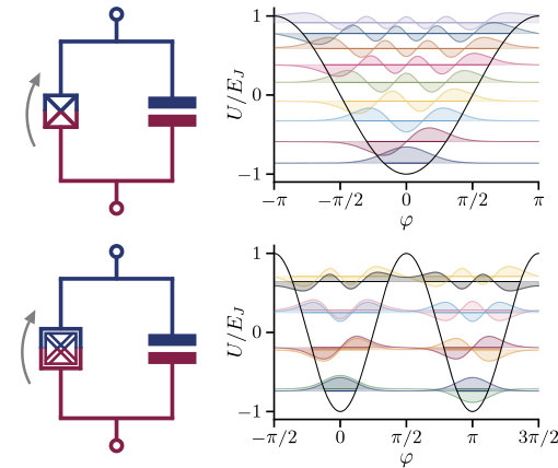 Figure 1
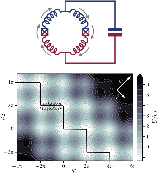 Figure 3
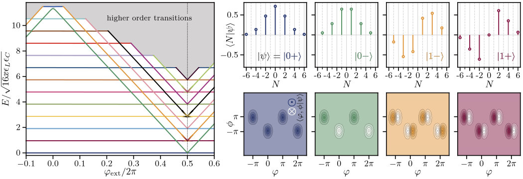 Figure 4
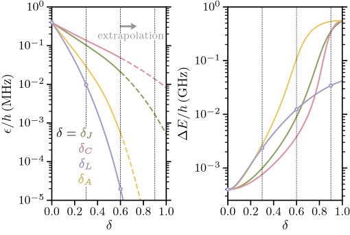 Figure 5
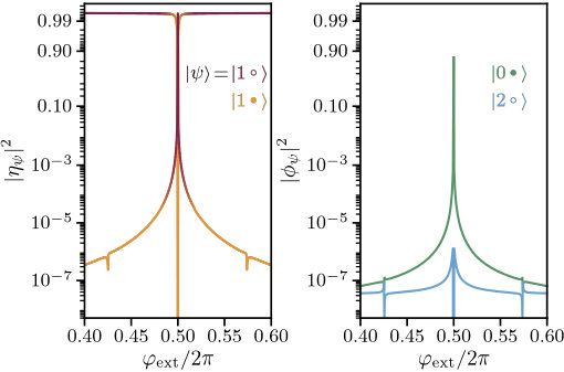 Figure 7
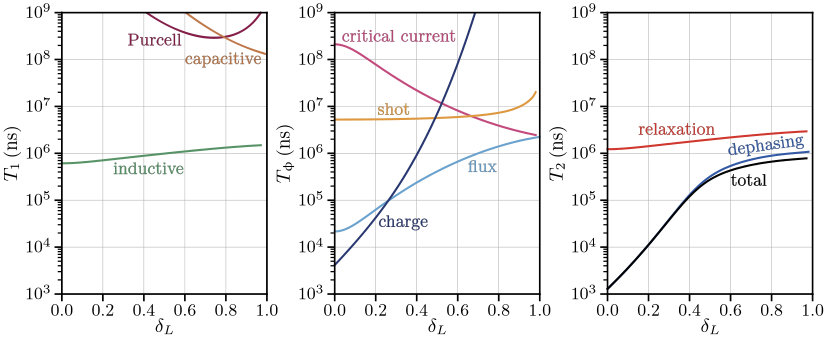 Figure 8
| 15 GHz | 2 GHz | 1 GHz | 0.02 |
| Loss channel | Quality factor | (ms) | ||||
|---|---|---|---|---|---|---|
| Capacitive | ||||||
| Inductive | ||||||
| Purcell | ||||||
| Quasiparticle | ||||||
| Dephasing channel | Spectral density amplitude | (ms) | ||||
| Charge | ||||||
| Flux | ||||||
| Shot | ||||||
| Critical current | ||||||
Peer Reviews
No public reviews on file for this paper yet. If you reviewed it on a platform where reviews are public (OpenReview, ICLR, NeurIPS, ICML), you can paste yours below so the community can read it here.
Videos
No videos yet. Explain this paper in a talk, walkthrough, or lecture? Add one.
††thanks: Current Address: QUANTIC Team, INRIA Paris, 2 rue Simone Iff, 75012 Paris, France
Superconducting circuit protected by two-Cooper-pair tunneling
W. C. Smith
A. Kou
X. Xiao
U. Vool
M. H. Devoret
Departments of Applied Physics and Physics, Yale University, New Haven, CT 06520, USA
Abstract
We present a protected superconducting qubit based on an effective circuit element that only allows pairs of Cooper pairs to tunnel. These dynamics give rise to a nearly degenerate ground state manifold indexed by the parity of tunneled Cooper pairs. We show that, when the circuit element is shunted by a large capacitance, this manifold can be used as a logical qubit that we expect to be insensitive to multiple relaxation and dephasing mechanisms.
I Introduction
I.1 Motivation
Superconducting circuits are widely recognized as a powerful potential platform for quantum computation and now stand at the frontier of quantum error correction Devoret and Schoelkopf (2013). Future progress will likely stem from two complementary strategies: (i) active error correction characterized by measurement-based Kelly et al. (2015); Ristè et al. (2015); Ofek et al. (2016) and autonomous Murch et al. (2012); Shankar et al. (2013); Leghtas et al. (2015); Puri et al. (2017) stabilization, and (ii) passive error correction characterized by protected qubits (Douçot and Ioffe, 2012, and references therein). We address strategy (ii) in this article by designing an experimentally accessible protected qubit.
The transmon qubit Koch et al. (2007) has proven to be a remarkably successful prototype of a protected qubit. Its circuit (depicted in Fig. 1a) contains a Josephson junction whose potential energy is , with being the tunneling energy and being the superconducting phase across the junction. The large shunt capacitance imposes a large effective mass for the analogous “particle in a box,” confining the low-energy wavefunctions near , the only minimum for . This confinement suppresses the susceptibility of the qubit to offset charge noise and renders the energy spectrum approximately harmonic with level spacing much smaller than (see Fig. 1b). On the other hand, circuit elements with degenerate phase states that only allow tunneling of pairs of Cooper pairs, meaning their potential energy is , have been developed in recent years as a building block for topologically protected qubits Douçot and Vidal (2002); Gladchenko et al. (2009). In this article, we propose a transmon-like qubit with additional protection from environmental noise by combining the large shunt capacitance of the transmon with such a circuit element (the cross-hatched box in Fig. 1c). In this case, the wavefunctions are localized near (see Fig. 1d), resulting in a nearly degenerate harmonic level arrangement. While the detrimental effects of offset charge noise are similarly suppressed in this circuit, sensitivity of the qubit to other decoherence mechanisms is also reduced, owing to the conservation of Cooper pair number parity.
In this article, we introduce a few-body transmon-type qubit where the charge carriers are exclusively pairs of Cooper pairs. Our central result is that there exists an experimentally attainable parameter regime for which conservative predictions of relaxation and dephasing times exceed ms, i.e. an order of magnitude higher than those of typical transmons, given the same environmental noise Rigetti et al. (2012); Wang et al. (2019). In the remainder of Sec. I, we describe a toy model for the protected qubit. We proceed by analytically and numerically examining the Hamiltonian for the full superconducting circuit in Sec. II. Our attention in Sec. III then turns to properties of the ground state manifold, which we envision using as a protected qubit. A brief discussion about the concept of protection and examples of protected qubits, as well as our perspectives on readout and control, follows in Sec. IV. Finally, we summarize our results in Sec. V.
I.2 element
We first examine the advantages of the ideal circuit in Fig. 1c as a protected qubit. This circuit can be viewed as a Josephson-junction-like element (the cross-hatched box) shunted by a capacitance. Pairs of Cooper pairs are the only charge excitations permitted to tunnel through this element Douçot and Vidal (2002). In the Cooper pair number basis, the potential energy assumes the form
[TABLE]
where is the effective tunneling energy of the process. This expression follows from the conjugacy relation , where is the number of Cooper pairs that have tunneled. The invariance of the potential under translations in by multiples of implies that half-fluxons are able to traverse the element.
The shunt capacitance and other charging effects produce a quadratic kinetic energy, yielding the Hamiltonian
[TABLE]
where is the charging energy and is the offset charge. This offset charge has been introduced due to the periodicity of the Hamiltonian in , which reflects the presence of a superconducting island in the circuit (as colored in Fig. 1c).
Since the circuit element only allows pairs of Cooper pairs to tunnel, the parity of the number of Cooper pairs that have tunneled is preserved under the action of the Hamiltonian. This property leads to two nearly degenerate ground states and , which only consist of even and odd Cooper pair number states, respectively Gladchenko et al. (2009). Since these states have no overlap in charge space (equivalently, they have opposite periodicity in phase space—see Fig. 1d), we have for any sufficiently local operator . Furthermore, the states 111This notation is chosen for consistency with Sec. II, where there is a correspondence to persistent current handedness. are respectively localized near (see Fig. 1d). Because these states have suppressed overlap in phase space for large (i.e. they are roughly inversely periodic in charge space), we have for similarly local . These are precisely the conditions for simultaneously suppressing spurious transitions and phase changes between the states Ioffe and Feigel’man (2002) [resembling a Gottesman-Kitaev-Preskill (GKP) encoding on a circle Gottesman et al. (2001)].
More concretely, the ground state splitting obeys
[TABLE]
for large (see App. A). The two ground state energies oscillate out of phase with one another in . Moreover, this shows that the splitting, as well as the charge dispersion, is exponentially suppressed in . Thus, the role of the shunt capacitance is to decrease the charging energy and hence mitigate offset charge noise, much like in the transmon qubit Koch et al. (2007).
II Superconducting circuit
II.1 Hamiltonian
We now detail the superconducting circuit necessary to practically implement the sought-after Josephson element. This circuit, depicted in Fig. 2a, is composed of two identical arms, each containing a Josephson junction in series with superinductances Manucharyan et al. (2009); Masluk et al. (2012), arranged in parallel Kitaev (2006); Brooks et al. (2013) and shunted by a large capacitance. These superinductances are split in half and placed on either side of the respective Josephson junctions to avoid large capacitances to ground. Kirchhoff’s current law allows us to treat the phases across the superinductances in series as equal. When the external magnetic flux threading the inductive loop reaches half of a flux quantum, i.e. when , the loop approximates the cross-hatched box in Fig. 1c. At this particular bias point, a Cooper pair can only tunnel through one of the Josephson junctions if it is accompanied by another Cooper pair tunneling through the other junction (in either direction). Conversely, a fluxon traversing a single Josephson junction corresponds to a half-fluxon traversing the whole element.
We consider the symmetric and antisymmetric combinations of superconducting phase coordinates
[TABLE]
and their conjugate charges in numbers of Cooper pairs. Note that the prefactor in the definition of is chosen to bring the coordinate into agreement with the phase drop across the inductive loop in the limit that vanishes. The Hamiltonian reads
[TABLE]
where and are the single junction charging and tunneling energies, is the inductive energy of each superinductance, is the ratio of the junction capacitance to the shunt capacitance, and is the offset charge on the superconducting island (see Fig. 2a).
From this expression, it is clear that this circuit has three strongly coupled modes. The mode is flux dependent and is strongly and nonlinearly coupled, via the Josephson junctions, to the mode. The mode is offset charge dependent and strongly but linearly capacitively coupled to the mode. Our analysis and the effects observed in the remainder of this article require the parameter regime , , and 222Specifically, the theory in Sec. II.2 breaks down at and the protection in Sec. III breaks down for .. In particular, the parameters chosen for numerical simulations are listed in Tab. 1 and are similar to those of recent fluxonium devices Manucharyan et al. (2009); Earnest et al. (2018).
II.2 Semiclassical theory
In order to gain insight into the structure of the Hamiltonian in Eq. 2, we briefly revisit its potential energy in the -plane, which is plotted in Fig. 2b for . The cosine terms in the potential form a two-dimensional “egg carton” of wells. The minimum of the quadratic term in the potential occurs at , which generally falls between adjacent diagonal ridges of cosine wells. At the special value of , these two ridges are degenerate. Near this value of the external flux, we consider the path of the system between neighboring potential minima by numerically solving for the three-dimensional instanton Matveev et al. (2002) trajectory (see App. B).
We then constrain the system to this maximally probable tunneling path. For the parameters mentioned above, this path is well-described by
[TABLE]
where is a small parameter 333The main discrepancy between the approximate path in Eq. 3 and the calculated path in Fig. 2b is the sharp bending near the minima, which arises due to coupling to the variable.. Plugging this expression into the Hamiltonian in Eq. 2, approximating the resulting one-dimensional potential by the first few terms in its Fourier series, and Taylor expanding about yields with
[TABLE]
to leading order. Here, and we have discarded terms higher than the second harmonic or (see App. B for additional terms). This treatment exposes the “ nature” of the potential at , where the term vanishes. By comparison to Eq. 1, we see that the added complication is that the mode is strongly coupled to the mode. The resulting hybridization is a central ingredient to understanding properties of the system beyond the ground state manifold (see Sec. II.4).
We comment that this approximation neglects quantum fluctuations that are perpendicular to the path in Eq. 3. This is consequently a semiclassical approximation: we have minimized the energy of the system with respect to the dynamical coordinate orthogonal to the trajectory Matveev et al. (2002). Moreover, from Fig. 2b, it is clear that the approximation we have made is that fluxons traverse a single Josephson junction at a time.
II.3 Energy spectrum
From numerical diagonalization of Eq. 2 (see App. C), we obtain the dependence of the energy levels on external flux as shown in Fig. 3a Smith et al. (2016). At (the dashed line in Fig. 3a), the spectrum resembles a doubled harmonic oscillator with energy . Once deviates from , half of the energy levels increase in energy linearly with slope 444This term is simply the potential energy at relative to that at (with ) found from Eq. 4.. The other half of the energy levels form a flux-independent harmonic ladder.
We can understand this level structure as that of two emergent modes (see also App. D). The first mode is flux-dependent and its excitations correspond to the number of magnetic flux vortices, or fluxons, enclosed by the inductive loop in Fig. 2a. In turn, the number of enclosed fluxons identically maps onto the magnitude and chirality of the circulating persistent current in the inductive loop. The second mode is flux-independent and its excitations correspond to quantized charge density oscillations, or plasmons, across the inductive loop/shunt capacitance in Fig. 2a. Each plasmon involves the two superinductances (energy in parallel) and the shunt capacitance (energy ), and hence has energy . Hereafter, we refer to these modes as the “fluxon mode” and the “plasmon mode,” respectively 555We comment that the Aharonov-Bohm effect manifests itself in this circuit through the fluxon mode, in which charge carriers circle a pinned flux. Conversely, the Aharonov-Casher effect involves the plasmon mode, in which flux vortices circle a pinned charge.. Additionally, we assign the labels |m\,\text{\raisebox{1.72218pt}{\scriptscriptstyle\bullet}}\,\rangle to the lowest-energy states, where denotes the number of plasmons and (or ) denotes the presence (or absence) of a fluxon excitation relative to the ground state 666Here we restrict the Hilbert space to the two fluxon states with lowest energy.. Note that the fluxon placeholder indices are defined by
[TABLE]
where (as in Sec. I.2) and the index represents the persistent current direction. This labeling serves the purpose of assigning quantum numbers consistently for all external flux values (see the colors in Fig. 3a 777Note that the coloring changes for only the odd-numbered plasmon states, due to the fact that the eigenstate with even overall parity has lower energy for each plasmon state, and that the overall parity includes both a plasmon and a fluxon component.), except the particular case that we do not focus on.
II.4 Wavefunctions
Calculated charge wavefunctions and phase wavefunctions , obtained from numerical diagonalization of Eq. 2, are shown in Figs. 3b, 3c for the four lowest-energy eigenstates at . Roughly, the phase wavefunctions are computed by projection of the coordinate and a Fourier transform to the -plane, while the charge wavefunctions are computed by projection of the coordinate and constraint to the trajectory in Eq. 3 (see App. C for details).
The charge wavefunctions are grid states with Fock-state envelopes Gottesman et al. (2001); Bell et al. (2014). For fluxon excitation index , these grid states are superpositions of even/odd Cooper pair number states 888The correspondence between Cooper pair number parity and the symmetry of the phase wavefunction can be seen from the -periodicity/-antiperiodicity of and Devoret (1997).. Additionally, corresponds to the order of the Fock state envelope. Note that a logical qubit encoded in and is protected from spurious transitions except those mediated by operators that flip Cooper pair parity.
On the other hand, the phase wavefunctions are approximately Fock states localized within the potential energy wells (see Sec. II.2) Earnest et al. (2018). The fluxon index denotes whether the state is a symmetric (bonding) or antisymmetric (antibonding) superposition of states localized within opposite ridges of potential wells. These ridges correspond to persistent currents of opposite chirality, and hence also to the absence/presence of a fluxon in the inductive loop of the circuit Dempster et al. (2014). In this picture, refers to the Fock order of the localized states. Finally, operators that flip Cooper pair parity correspond to odd functions of or functions of with period an odd division of , which can be seen from Fig. 3c to mediate the transition
III Qubit
In Sec. II, we analyzed the multi-mode Hamiltonian describing the superconducting circuit in Fig. 2a. Numerical diagonalization of this Hamiltonian showed the emergence of a linear plasmon mode and a nonlinear fluxon mode 999The number of plasmon and fluxon modes form the rows and columns of a crude superconducting circuit periodic table. Charge-based qubits such as the transmon have one plasmon mode and no fluxon modes. Flux-based qubits such as the fluxonium have one fluxon mode and no plasmon modes. This circuit has two plasmon modes (one of which is neglected at low frequencies) and one fluxon mode. The larger resulting Hilbert space is the resource used to achieve protection.. In this section, we consider the properties of the logical qubit formed by , the two lowest-energy eigenstates at , which generalizes to \{|0\,\text{\raisebox{1.72218pt}{\scriptscriptstyle\circ}}\,\rangle,|0\,\text{\raisebox{1.72218pt}{\scriptscriptstyle\bullet}}\,\rangle\} away from .
III.1 Matrix elements
To better elucidate which types of operators can and cannot induce transitions between the two states of the qubit, we examine the relevant matrix elements corresponding to capacitive and inductive coupling. This discussion is particularly relevant to understanding the expected dominant loss mechanisms (Sec. III.3) and designing a measurement and control apparatus that does not directly couple to the qubit (Sec. IV.3).
For capacitive coupling, a generic voltage couples to the superconducting island of the circuit in Fig. 2a via a gate capacitance and will append the term
[TABLE]
to the Hamiltonian in Eq. 2, in addition to dressing the shunt capacitance. This voltage may be a degree of freedom of another mode in the embedding circuit, a noise source, or an ac drive. We therefore see that the susceptibility of undergoing a transition from the ground state, due to capacitive coupling to the qubit island, is directly related to the matrix element \langle\psi|\eta|0\,\text{\raisebox{1.72218pt}{\scriptscriptstyle\circ}}\,\rangle.
For inductive coupling, a generic current couples to the circuit via a small inductance shared with the inductive loop, which adds the term
[TABLE]
to the Hamiltonian in Eq. 2. Here, is the reduced magnetic flux quantum and is the superinductance in each arm of the qubit (i.e. ). Like the voltage source, this current may represent an internal or environmental degree of freedom. We see that the susceptibility of undergoing a transition from the ground state, due to inductive coupling to the inductive loop, is related to the matrix element \langle\psi|\phi|0\,\text{\raisebox{1.72218pt}{\scriptscriptstyle\circ}}\,\rangle.
Limiting the Hilbert space to the six lowest-energy eigenstates , we numerically compute the normalized matrix elements
[TABLE]
from the ground state |0\,\text{\raisebox{1.72218pt}{\scriptscriptstyle\circ}}\,\rangle for the operators . Results are plotted in Fig. 4. Note that and , so we may reasonably consider these as transition probabilities via .
We see from Fig. 4a that transitions mediated by capacitive coupling to the qubit island are only allowed from |0\,\text{\raisebox{1.72218pt}{\scriptscriptstyle\circ}}\,\rangle to |1\,\text{\raisebox{1.72218pt}{\scriptscriptstyle\circ}}\,\rangle. These selection rules result from the decoupling of the even and odd Cooper pair number parity manifolds (see App. D). Most importantly, transitions between qubit states are forbidden, meaning capacitive coupling offers a promising ingredient for indirect qubit measurement and control (see Sec. IV.3). Conversely, inductive coupling to the inductive loop of the qubit permits transitions between |0\,\text{\raisebox{1.72218pt}{\scriptscriptstyle\circ}}\,\rangle and |0\,\text{\raisebox{1.72218pt}{\scriptscriptstyle\bullet}}\,\rangle in the vicinity of , as shown in Fig. 4b. This effect arises because the operator induces transitions between the Cooper pair parity manifolds, as can be seen from the Fourier series for Eq. 3. As a consequence, we expect that relaxation of the qubit will be primarily due to inductive loss in the superinductances (see Sec. III.3).
III.2 Disorder
A highly symmetric superconducting circuit is usually fragile in view of unavoidable fabrication imperfections Dempster et al. (2014). The symmetry of our circuit involving the two inductive arms in Fig. 2a may be broken in three parameters: the Josephson energies of the junctions, the capacitances of the junctions, or the superinductances. To analyze these effects, we numerically diagonalize Eq. 2 and examine the energy splitting 101010The energy splitting is evaluated at . as well as the charge dispersion of the manifold at . A dimensionless quantity is introduced to parameterize the extent of asymmetry in all three cases, and the -dependence of the energies and is studied.
III.2.1 Disorder in
We model disorder in the Josephson energies of the junctions by allowing the values of to deviate. We therefore set the left and right junction tunneling energies to , respectively, where is the aforementioned asymmetry parameter. The Hamiltonian in Eq. 2 is perturbed by the term
[TABLE]
See Fig. 5 for a plot of and as a function of . The important feature in these plots is that the charge dispersion decreases exponentially while the splitting increases exponentially with 111111The extrapolation of the charge dispersion as a function of the disorder beyond is due to numerical instabilities inherent to low-energy quantities paired with disappearance of an efficient diagonalization basis for large disorder. This is particularly obvious in the vicinity of , at which point the number of modes of the circuit reduces from three to two.. These features arise from the effective Hamiltonian in Eq. 4 being accompanied by -periodic terms in the presence of disorder. In this case of disorder in , the approximations in Sec. II.2 lead to with
[TABLE]
which evidently permits the tunneling of single Cooper pairs across the element. The resulting qubit retains characteristics of the symmetric circuit as well as the asymmetric/transmon-like circuit.
III.2.2 Disorder in
Analogous to Sec. III.2.1, we set the left and right junction charging energies to , respectively. Aside from dressing the charging energy, the Hamiltonian in Eq. 2 inherits the term
[TABLE]
whose effect on the qubit manifold is plotted in Fig. 5.
This form for capacitive disorder is assumed due to the fact that, if , then the product is kept constant for both junctions under the effects of disorder. This corresponds to the physical case where the junction plasma frequencies are fixed by oxidation, but their areas differ due to fabrication imperfections. Here, the junction areas are because . The consequences of area disorder are plotted in Fig. 5.
III.2.3 Disorder in
Following the same procedure, we set the left and right superinductance inductive energies to , respectively. This form is taken in order to fix the total linear inductance in the loop. Aside from dressing the inductive energy, the Hamiltonian in Eq. 2 is perturbed by
[TABLE]
Note in Fig. 5 that the charge dispersion and energy splitting follow the same general trend for inductive disorder as for the other three. The key difference is that the charge dispersion decreases more quickly than for any other form of disorder. Oppositely, the splitting is initially the same as for area disorder, but the slope decreases in . We conclude that disorder allows us to engineer a circuit with a sufficiently non-degenerate ground state manifold whose charge dispersion is largely suppressed. For reasons that will become clear in Sec. III.4, these features are extremely valuable for designing a qubit that is protected from dephasing.
III.3 Relaxation
We model loss due to an arbitrary channel using Fermi’s Golden Rule. This gives us the relaxation rate, including both emission and absorption, of
[TABLE]
In this expression, is the operator of the circuit coupling to a noisy bath variable , the noise spectral density of which is given by . Note that . In this subsection, we calculate the relaxation rates for the expected dominant loss mechanisms of the qubit based on numerical diagonalization of the full Hamiltonian in Eq. 2. We perform this calculation for various degrees of inductive disorder (see Fig. 5).
We consider four possible loss channels for the qubit: capacitive loss, inductive loss, Purcell loss, and quasiparticle tunneling Pop et al. (2014). Capacitive loss involves dielectric dissipation in the Josephson junction capacitances. In this case, we have \mathcal{O}=2eN_{i}=2e\big{[}n\pm\frac{1}{2}(N-\eta)\big{]} for the charge across the -th junction and for a bath voltage with
[TABLE]
Here, is the junction capacitance, is the temperature, and is a frequency-dependent quality factor Braginsky et al. (1987) with nominal value Wang et al. (2015) (see App. E for more details).
Depending on the specific implementation, inductive loss may occur within the superinductances via quasiparticle tunneling Pop et al. (2014). This situation can be modeled by taking for the flux across the -th superinductance and for a bath current with
[TABLE]
In this expression, is the -th superinductance and is a frequency-dependent quality factor with nominal value Pop et al. (2014). As shown in App. E, this frequency dependence is included to extrapolate to small qubit transition frequencies.
Loss due to the Purcell effect should mainly arise from coupling of the qubit to the plasmon mode, which we model as dielectric loss in the shunt capacitance. As such, we have and for a bath voltage with the same noise spectral density as Eq. 7, but with replaced by .
Finally, quasiparticle tunneling is expected to occur across either Josephson junction and contribute to qubit relaxation Pop et al. (2014). In this case, we have for the -th junction and the noise spectral density
[TABLE]
with being the dissipative part of the Josephson junction admittance Catelani et al. (2011) (see App. E for the explicit form). Note that this admittance scales linearly in both and the quasiparticle density defined relative to that of Cooper pairs.
The calculated relaxation rates and the corresponding components of Eq. 6 are shown in Tab. 2 for all four loss channels at . For both capacitive and inductive loss, we note that measurements have not yet been performed using qubits with extremely small energy splittings, and the calculation presented here relies on an extrapolation to such frequencies. A key feature is the complete absence of quasiparticle loss, as in the fluxonium qubit Pop et al. (2014). Additionally, we see that the asymmetric qubit is marginally less susceptible to inductive loss than the symmetric qubit. This improvement comes at the cost of the susceptibility to capacitive and Purcell loss. However, we emphasize that the lifetimes shown in Tab. 2 are conservative estimates that demonstrate ms, which is at least competitive with state-of-the-art qubit implementations Rigetti et al. (2012); Barends et al. (2013); Pop et al. (2014); Bell et al. (2014); Yan et al. (2016); Groszkowski et al. (2018).
III.4 Pure dephasing
In this subsection, we examine the dependence of the qubit transition energy on various system parameters corresponding to different dephasing mechanisms. We estimate the dephasing times due to offset charge noise, external flux noise, photon shot noise in the plasmon mode, and critical current noise. The noise spectral densities are all assumed to be and hence given by , where is the amplitude, with the sole exception of shot noise whose spectral density is assumed to be Lorentzian.
III.4.1 Charge noise
In the case of perfect symmetry, the charge dispersion is identically mapped to . As a consequence, resilience to dephasing from offset charge noise demands a high degree of degeneracy, making experimental implementation difficult. Fortunately, this issue can be avoided by introducing inductive disorder into the system (see Sec. III.2.3). In the slow-varying limit for charge noise, the pure dephasing rate is bounded by
[TABLE]
where e is Euler’s number Koch et al. (2007). In Tab. 2, we see that this yields a strict bound on the decoherence time in the case of perfect symmetry, which is greatly alleviated in the presence of inductive disorder. Note that this estimate does not explicitly involve because the slow-varying limit has been taken where the offset charge assumes a random value for each measurement, but does not fluctuate within a given measurement.
III.4.2 Flux noise
At , the qubit manifold is only susceptible to external flux noise to second order. However, one can easily obtain 121212For example, this can done using the double-well Hamiltonian for in the vicinity of , where the two spin states correspond to . One then has the flux-dependent splitting and hence (at ). the relation (at ), which shows that insensitivity to flux-noise-induced dephasing requires sufficiently weak degeneracy, at odds with the requirement for resilience to charge noise. Once more, introducing inductive disorder avoids this issue. Neglecting components that depend on details of the implementation, the pure dephasing rate Cottet (2002) is bounded by
[TABLE]
where is the amplitude of the noise spectral density Quintana et al. (2017); Kou et al. (2017) for . As in the case of charge noise, this places a stringent limit on the decoherence time of the qubit in the absence of inductive disorder, as we see in Tab. 2.
III.4.3 Shot noise
We expect the dominant contribution to dephasing due to thermal photons to arise from coupling to the plasmon mode. This mode has an angular frequency and an occupation with mean given by . To this end, we place a bound on the pure dephasing time using the expression Rigetti et al. (2012)
[TABLE]
where is the dispersive shift of the qubit on the plasmon mode and is the linewidth of the plasmon mode. Note that, as in Sec. III.3, we use the frequency-dependent dielectric quality factor with nominal value Wang et al. (2015). In all cases, this form of noise is not expected to limit the decoherence time of the qubit (see Tab. 2).
III.4.4 Critical current noise
The final dephasing mechanism we investigate is critical current noise, or fluctuations in the Josephson energy . As in the case of flux noise, we discard factors that are sensitive to experimental details and take the dephasing rate to be bounded by Cottet (2002)
[TABLE]
where is the amplitude of the noise spectral density van Harlingen et al. (2004) for . As in the case of photon shot noise, we do not expect critical current noise to place a strict bound on the decoherence time (see Tab. 2).
At this point, it is clear that inductive asymmetry constitutes a necessary ingredient in the protection of this qubit. In light of Eq. 5, we attribute this to the resulting hybridization of the and modes, which are not directly coupled in the symmetric case (see Eq. 2). The fluxon transition between the qubit states inherits some character of the plasmon transition, thereby breaking the correspondence between and and reducing the flux matrix element .
IV Discussion
IV.1 Protection
We have proposed a superconducting circuit whose ground state manifold can be made protected, at the Hamiltonian level, from multiple common sources of noise. Here we describe some of the other strategies for achieving protection. The simplest manifestations involve improving quality factors associated with coupling to different thermal baths Martinis et al. (2005); Houck et al. (2008); Barends et al. (2013) and reducing noise spectral densities for different Hamiltonian parameters Paik et al. (2011); Rigetti et al. (2012); Kumar et al. (2016). At a higher level, a popular approach to suppressing qubit relaxation has been to localize wavefunctions in disparate regions of phase space to lessen transition matrix elements Pop et al. (2014); Bell et al. (2014); Earnest et al. (2018); Lin et al. (2018). On the other hand, delocalization of the same wavefunctions has been shown to mitigate dephasing effects by reducing qubit sensitivity to Hamiltonian parameters van der Wal et al. (2000); Vion et al. (2002); Koch et al. (2007); Manucharyan et al. (2009); Steffen et al. (2010); Yan et al. (2016). Superconducting circuits with multiple degrees of freedom whose qubit wavefunctions are both localized and delocalized combine both of these approaches. In these circuits, quantum information is diffused among constituent local degrees of freedom, providing protection from local perturbations. The many-body limit promises topological protection Douçot and Vidal (2002); Ioffe and Feigel’man (2002); Douçot et al. (2003); Kitaev (2006), in which global operators are necessary to manipulate logical qubits, but the few-body case described here offers an experimentally realistic approximation Cottet et al. (2002); Gladchenko et al. (2009); Brooks et al. (2013); Bell et al. (2014); Dempster et al. (2014); Kou et al. (2017); Groszkowski et al. (2018). In the following subsection, we outline the key differences between our circuit and similar proposals.
IV.2 Comparison to other protected qubits
IV.2.1 Heavy fluxonium
The heavy fluxonium Earnest et al. (2018); Lin et al. (2018), in which a conventional fluxonium qubit is shunted by a large capacitance, shares many similar features with the circuit in Fig. 2a. In fact, our circuit roughly reduces to that of the conventional fluxonium in the extremely asymmetric limit of , and the eigenstates of both circuits are similarly represented in terms of persistent currents. The two main differences are that our circuit contains an additional small Josephson junction and that the shunt capacitance is placed across the junction along with a subset of the array junctions. An analogy can be drawn between in our circuit and the shunt capacitance in the heavy fluxonium, because they both suppress the qubit transition frequency. Physically, the qubit eigenstates differ when these analogous parameters fall to small values. While the eigenstates collapse to Cooper pair number parity states in our circuit, this is not true for the heavy fluxonium because the variable is not compact.
IV.2.2 Rhombus qubit
The circuit in Fig. 2a bears resemblance to the rhombus Blatter et al. (2001), with two central differences. First, in the rhombus, the superinductances are replaced by single Josephson junctions, or arrays of a few larger junctions Douçot and Ioffe (2012); Bell et al. (2014). This changes the parameter regime of the circuit from to , decreasing the amplitude of the term in the Hamiltonian. Second, the shunt capacitance is replaced by a gate capacitance to a voltage source Bell et al. (2014). This is akin to substituting an electrostatic gate for a shunt capacitance to obtain the Cooper pair box Vion et al. (2002) from the transmon Koch et al. (2007); overall suppression of the charge dispersion is traded for the ability to bias the circuit at its charge sweet spot.
Finally, the rhombus by itself is not designed to be a protected qubit. Rather, when multiple rhombi are arranged into a one-dimensional chain (or a two-dimensional fabric), the ground states are eigenstates of a nonlocal operator, which provides topological protection Douçot and Vidal (2002); Ioffe and Feigel’man (2002); Douçot et al. (2003); Douçot and Ioffe (2012). On one hand, our qubit does not require such scaling to achieve protection. On the other hand, the protection we predict is inherently susceptible to local perturbations (see Secs. III.3, III.4).
IV.2.3 0- qubit
The 0- qubit Brooks et al. (2013) also has a similar superconducting circuit to that in Fig. 2a, but with three essential distinctions. First, the pairs of superinductances on each arm of the circuit are combined, altering the embedding capacitance matrix, in particular the capacitances to ground. Second, there is the addition of a second large capacitance shunting the inductive loop between its two horizontally oriented nodes. When this second capacitance is precisely , this permits the exact decoupling of the mode from the mode in Eq. 2. Third, the 0- qubit is operated in a parameter regime where , as opposed to our circuit, where Dempster et al. (2014). This additional order of magnitude in the superinductance may prove marginally less accessible experimentally Manucharyan et al. (2009); Masluk et al. (2012).
Notably, the inductive loop in the 0- qubit is threaded with at its working point instead of . This leads to a substantial change in the physics of the ground state manifold; and are approximately localized in distinct potential wells Dempster et al. (2014). In our case, these states are approximately the symmetric and antisymmetric superpositions of the localized wavefunctions, which are themselves localized in distinct Cooper pair number parities.
IV.3 Readout and control
Protected qubits face the serious obstacle of realizing state manipulation and measurement while remaining sufficiently isolated from their environments to preserve their coherence. We envision performing readout and control using an ancillary mode structure, which enables cascaded dispersive readout and Raman indirect transitions, as outlined below.
For readout, we aim to exploit the sizable native dispersive shift of the qubit on the plasmon mode, (see Sec. III.4.3). Unfortunately, the small anharmonicity, which is at most of order , of the plasmon mode makes readout of the plasmon mode using a linear mode (e.g. a microwave cavity) difficult. As a remedy, we propose introducing an ancillary anharmonic mode by which to measure the plasmon state. In this scheme, a dispersive interaction will be mediated by the ancillary mode between the readout and plasmon modes, thereby enabling dispersive measurement with two readout tones Kirchmair et al. (2013).
The above-mentioned ancillary anharmonic mode will also be useful for control of the protected qubit. As shown in Sec. III.1, direct transitions mediated by capacitive coupling to the qubit superconducting island are strictly forbidden in the symmetric case, and weakly forbidden in the asymmetric case. Note that this coupling method is chosen to minimize the contributions to decoherence resulting from the introduction of the readout/control circuit. For manipulation, we therefore propose transitioning through the or state, as in a conventional system. An additional complication is that, even in the presence of inductive asymmetry, the joint fluxon-plasmon transitions and are forbidden.
Using an ancillary mode based on the Superconducting Nonlinear Asymmetric Inductive eLement (SNAIL) Frattini et al. (2017), it is possible to engineer selection rules where the joint fluxon-plasmon transitions are weakly permitted while the qubit transition is left unaffected, as has recently been demonstrated in a fluxonium qubit Vool et al. (2018). This stems from the feature of the SNAIL that allows, at specific flux biases, third-order nonlinearities without fourth-order nonlinearities. If we parameterize the broken selection rule using , the matrix element of relative to , then the gate speed via sequential direct transitions and a stimulated Raman transition is estimated to be and , respectively Steck (2019). Here, is the detuning of the Raman drive from the intermediate state and is the -pulse time Chow et al. (2010). This also introduces an additional Purcell loss channel (and vice versa), which corresponds to the relaxation time . We therefore expect gate speeds to be slowed by a factor of while lifetimes are kept in the millisecond range.
V Conclusion
In summary, we have designed a few-body superconducting circuit in which the charge carriers are well-approximated by pairs of Cooper pairs at a particular bias point. The Josephson tunneling element that supports these charge carriers is characterized by a term in the Hamiltonian, whose emergence we have shown analytically. Our numerical simulations supplement these arguments and demonstrate protection against a variety of common relaxation and dephasing sources. We find that this protection is substantially enhanced in the presence of disorder. Finally, we compared our circuit to similar proposals and offered our perspectives on readout and control.
As a final remark, we comment that engineering a circuit whose potential energy is dominated by a term opens the door to more exotic designs with potential energies of the form , with , which could be obtained by introducing additional loops in the circuit. These could be tremendously valuable for quantum simulation, realizing nearly degenerate ground state manifolds with greater multiplicities, or performing degeneracy-preserving measurements of photon number parity Cohen et al. (2017).
Acknowledgements.
We thank J. Cohen, S. M. Girvin, L. I. Glazman, M. Mirrahimi, R. J. Schoelkopf, K. Serniak, and S. Shankar for their insights. This work was supported by the Army Research Office Grant No. W911NF-14-1-0011 and W911NF-18-1-0212. W.C.S. was supported by DoDMURI award No. FP057123-C. Facilities use was supported by the Yale Institute of Nanoscience and Quantum Engineering under National Science Foundation Grant No. MRS1119826.
Appendix A Mathieu equation
The time-independent Schrödinger equation for Eq. 1 assumes the form
[TABLE]
Using the trial function , this equation becomes
[TABLE]
which is the Mathieu equation Meixner et al. (1980); Koch et al. (2007). The -th eigenenergy is given by
[TABLE]
where denotes the Mathieu characteristic value and is an integer that sorts the eigenvalues. The crucial difference between this solution and that for the Cooper pair box is that the characteristic exponent is replaced by Koch et al. (2007). This gives rise to the nearly degenerate ground states in the Hamiltonian in Eq. 1. In particular, for , we can use the asymptotic form of the Mathieu characteristic values to find
[TABLE]
with being the charge dispersion of the -th level. Importantly, for even values of , we have (neglecting constants and nonlinear terms) and . Additionally, the expression for the ground state splitting in Sec. I.2 is justified by
[TABLE]
and the fact that .
Appendix B Instanton treatment
The average tunneling trajectory between potential minima for the Hamiltonian in Eq. 2 can be found by examining an equivalent classical problem. This is done by inverting the potential and solving the classical equations of motion for a particle that starts at one maxima and ends at the other, each with zero kinetic energy Matveev et al. (2002). Consequently, this classical trajectory requires an infinite amount of time. The corresponding differential equations,
[TABLE]
are solved numerically. Carrying out the procedure in Sec. II.2, but retaining terms through the fourth harmonic and , results in the extended version of the effective Hamiltonian
[TABLE]
which clearly reduces to Eq. 4. At , we see that the dominant correction term is of the form . Moreover, we observe that the odd Fourier terms exactly vanish for the symmetric circuit at this flux bias, while the coefficients for the even Fourier terms decay roughly in powers of .
Appendix C Numerical diagonalization
For numerical diagonalization of either Eq. 2 or Eq. 4, we employ a charge basis for the mode in order to efficiently capture the dependence of the Hamiltonian on Devoret (1997). This is due to the exact periodicity of the Hamiltonian in , which inhibits the use of a harmonic oscillator basis to capture the multi-well physics apparent in Fig. 2b. For the and modes, we use harmonic oscillator bases. Explicitly, the full Hamiltonian in Eq. 2 can be written as
[TABLE]
after discarding constants, where and are bosonic creation/annihilation operators for the and modes, respectively. Additionally, the zero point fluctuation amplitudes \phi_{\text{zpf}}=\big{(}\frac{8\epsilon_{C}}{\epsilon_{L}}\big{)}^{1/4} and \eta_{\text{zpf}}=\frac{1}{2}\big{(}\frac{\epsilon_{L}}{x\epsilon_{C}}\big{)}^{1/4} have been introduced for convenience. The diagonalization basis is then
[TABLE]
with being the Cooper pair number eigenstates of the operator and being the photon number eigenstates of . For numerical convergence, the dimensions , , and are used, depending on the desired truncation accuracy. The remaining operators are written as
[TABLE]
in this basis, while the final cosine term in Eq. 8 has an exact matrix expression Smith et al. (2016), which we do not repeat here. Although the above discussion applies to the case of perfect symmetry, the discussion in Sec. III.2 allows a straightforward extension to the disordered case. Finally, we comment that, despite the high dimensionality of the matrix in Eq. 8, diagonalization can be made efficient by taking advantage of its sparsity.
Now we detail the method used to compute the wavefunctions and (up to an overall phase) for plotted in Figs. 3b, 3c. First, the coordinate space wavefunction is constructed using Devoret (1997) and the expressions for and as harmonic oscillator wavefunctions:
[TABLE]
where the complex coefficients are obtained by diagonalization (and consistent choice of overall phase). Then, the -dependence is removed by projection onto and normalization. This amounts to computing
[TABLE]
which is plotted in Fig. 3c. Next, the -dependence is removed by invoking Eq. 3. In this step, we project onto and normalize to obtain
[TABLE]
Finally, the Fourier transform of this function yields the charge wavefunctions
[TABLE]
which are plotted in Fig. 3b.
Appendix D Parity sectors
To explain the energy level structure at , we factor Eq. 4 into the form Aasen et al. (2016)
[TABLE]
The parity sectors are governed by the Hamiltonians
[TABLE]
In the above, and while and should be viewed as conjugate operators corresponding to pairs of Cooper pairs. Note that this expression is an exact reformulation of Eq. 4. In the limit that , we may Taylor expand the potential about and retain the first few terms. This step discards the effects of the offset charge, rendering and identical. We then decompose the linear part of the Hamiltonian into normal modes, which yields
[TABLE]
to leading order in . The corresponding transformation is given by
[TABLE]
Eq. 9 reveals two weakly anharmonic modes: the plasmon mode at the low frequency of and a junction self-resonant mode at the high frequency of . These modes are coupled by a quartic nonlinearity, which has the primary effect of inducing a Kerr shift on the junction self-resonant mode. At frequencies lower than , the energy level structure is that of a two-fold degenerate harmonic oscillator, in agreement with the simulated energy spectrum at (see the dashed line in Fig. 3a).
Appendix E Coherence estimates
To expand on Secs. III.3 and III.4, where relaxation pure dephasing times were calculated for four values of , we plot in Fig. 6 the results for the entire span of . In addition, in Fig. 6c we also plot the expected relaxation, pure dephasing, and decoherence times combining the effects of all considered channels. Here, the overall decoherence time is defined using the relation . We also note that, for the estimate of the dephasing rate due to charge noise, we do not use the extrapolation shown in Fig. 5a for the cases of disorder in , , and . Numerical instabilities are not encounted for disorder in until (which is outside the plotted range for both Fig. 5a and Fig. 6b).
In the remainder of this appendix, we describe the assumed frequency dependence of the three quality factors used for the relaxation time estimates in Sec. III.3. First, for the dielectric quality factor, we use the form Braginsky et al. (1987); Pop et al. (2014)
[TABLE]
so that the nominal value corresponds to measurements performed at the resonant frequency of Wang et al. (2015).
Second, for quasiparticle loss, the dissipative part of the admittance for a Josephson junction with tunneling energy is given Catelani et al. (2011) to be
[TABLE]
where is the resistance quantum, is the superconducting gap, and is the modified Bessel function of the second kind. This expression holds under the assumption that the quasiparticle bath is in thermal equilibrium at temperatures , which may not be correct, depending on the implementation Serniak et al. (2018). As we have seen, the matrix elements for quasiparticle loss vanish for this circuit, so this admittance has little bearing on our relaxation time estimates.
On the other hand, inductive loss has been suggested to occur due to quasiparticle tunneling across Josephson junctions that compose superinductances Pop et al. (2014). If we expect the frequency-dependence of the dissipative part of the admittance to agree between quasiparticle and inductive loss, then we arrive at
[TABLE]
so that the nominal value corresponds to measurements performed at the resonant frequency of .
The reference list from the paper itself. Each links out to its DOI / PubMed record.
- 1Devoret and Schoelkopf (2013) M. H. Devoret and R. J. Schoelkopf, Science 339 , 1169 (2013) . · doi ↗
- 2Kelly et al. (2015) J. Kelly, R. Barends, A. G. Fowler, A. Megrant, E. Jeffrey, T. C. White, D. Sank, J. Y. Mutus, B. Campbell, Y. Chen, Z. Chen, B. Chiaro, A. Dunsworth, I.-C. Hoi, C. Neill, P. J. J. O’Malley, C. Quintana, P. Roushan, A. Vainsencher, J. Wenner, A. N. Cleland, and J. M. Martinis, Nature 519 , 66 (2015) . · doi ↗
- 3Ristè et al. (2015) D. Ristè, S. Poletto, M.-Z. Huang, A. Bruno, V. Vesterinen, O.-P. Saira, and L. Di Carlo, Nat. Commun. 6 , 6983 (2015) . · doi ↗
- 4Ofek et al. (2016) N. Ofek, A. Petrenko, R. Heeres, P. Reinhold, Z. Leghtas, B. Vlastakis, Y. Liu, L. Frunzio, S. M. Girvin, L. Jiang, M. Mirrahimi, M. H. Devoret, and R. J. Schoelkopf, Nature 536 , 441 (2016) . · doi ↗
- 5Murch et al. (2012) K. W. Murch, U. Vool, D. Zhou, S. J. Weber, S. M. Girvin, and I. Siddiqi, Phys. Rev. Lett. 109 , 183602 (2012) . · doi ↗
- 6Shankar et al. (2013) S. Shankar, M. Hatridge, Z. Leghtas, K. M. Sliwa, A. Narla, U. Vool, S. M. Girvin, L. Frunzio, M. Mirrahimi, and M. H. Devoret, Nature 504 , 419 (2013) . · doi ↗
- 7Leghtas et al. (2015) Z. Leghtas, S. Touzard, I. M. Pop, A. Kou, B. Vlastakis, A. Petrenko, K. M. Sliwa, A. Narla, S. Shankar, M. J. Hatridge, M. Reagor, L. Frunzio, R. J. Schoelkopf, M. Mirrahimi, and M. H. Devoret, Science 347 , 853 (2015) . · doi ↗
- 8Puri et al. (2017) S. Puri, S. Boutin, and A. Blais, npj Quantum Inf. 3 , 18 (2017) . · doi ↗