Origin of nonclassical light emission from defects in multi-layer hexagonal boron nitride
Alexander Bommer, Christoph Becher

TL;DR
This study investigates the origin of non-classical light emission from defects in multi-layer hexagonal boron nitride, revealing that emitters are likely composed of two independent electronic transitions rather than pure single photon sources.
Contribution
It provides new evidence that defects in multi-layer hBN involve double electronic transitions, challenging previous assumptions of single photon emission.
Findings
Emitters are not pure single photon sources.
Each zero phonon line involves two independent electronic transitions.
Suggests a double defect nature of emitters in multi-layer hBN.
Abstract
In recent years, mono-layers and multi-layers of hexagonal boron nitride (hBN) have been demonstrated as host materials for localized atomic defects that can be used as emitters for ultra-bright, non-classical light. The origin of the emission, however, is still subject to debate. Based on measurements of photon statistics, lifetime and polarization on selected emitters we find that these atomic defects do not act as pure single photon emitters. Our results strongly and consistently indicate that each zero phonon line of individual emitters is comprised of two independent electronic transitions. These results give new insights into the nature of the observed emission and hint at a double defect nature of emitters in multi-layer hBN.
Click any figure to enlarge with its caption.
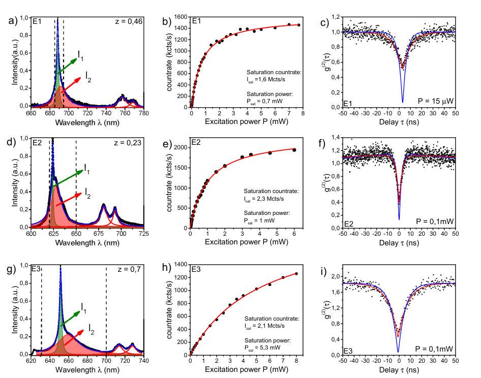 Figure 1
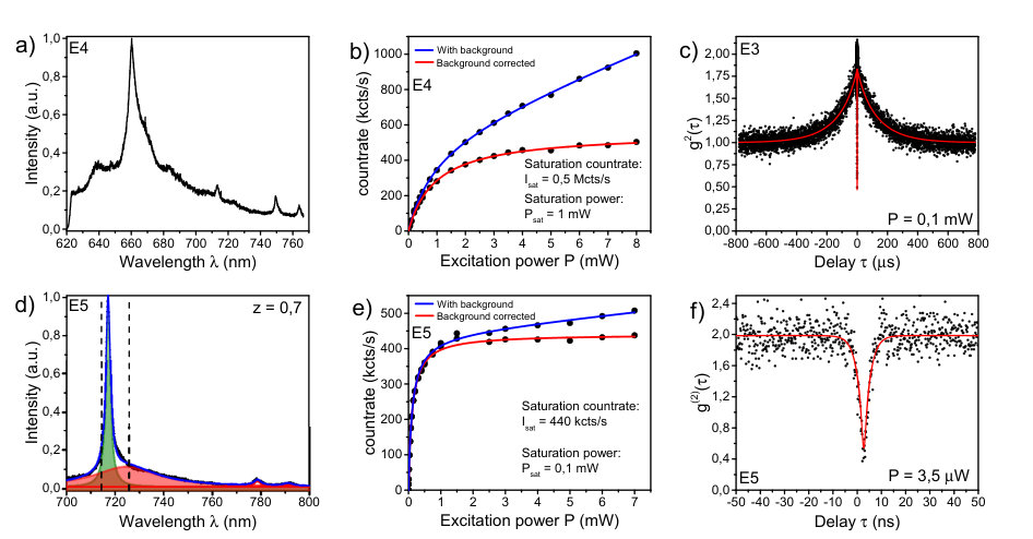 Figure 2
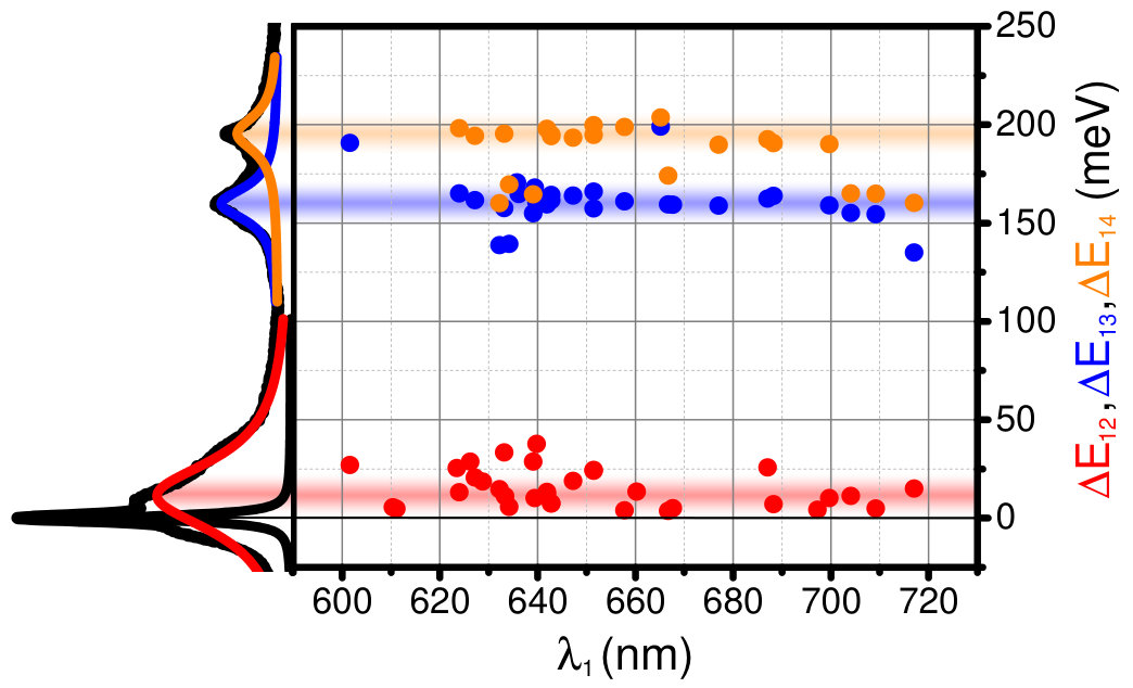 Figure 3
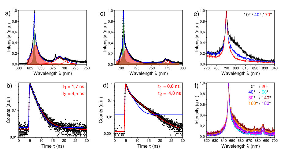 Figure 4
Peer Reviews
No public reviews on file for this paper yet. If you reviewed it on a platform where reviews are public (OpenReview, ICLR, NeurIPS, ICML), you can paste yours below so the community can read it here.
Videos
No videos yet. Explain this paper in a talk, walkthrough, or lecture? Add one.
Origin of nonclassical light emission
from defects in multi-layer hexagonal boron nitride
Alexander Bommer
Universität des Saarlandes, Fachrichtung Physik, Campus E2.6, 66123 Saarbrücken
Christoph Becher
Universität des Saarlandes, Fachrichtung Physik, Campus E2.6, 66123 Saarbrücken
Abstract
In recent years, mono-layers and multi-layers of hexagonal boron nitride (hBN) have been demonstrated as host materials for localized atomic defects that can be used as emitters for ultra-bright, non-classical light. The origin of the emission, however, is still subject to debate. Based on measurements of photon statistics, lifetime and polarization on selected emitters we find that these atomic defects do not act as pure single photon emitters. Our results strongly and consistently indicate that each zero phonon line of individual emitters is comprised of two independent electronic transitions. These results give new insights into the nature of the observed emission and hint at a double defect nature of emitters in multi-layer hBN.
I Introduction
Recently, two dimensional van der Waals materials have emerged as promising platforms for optoelectronics Srivastava2015 ; Palacios-Berraquero2016 ; Chakraborty2015 , candidates for future UV-LEDs Kenji2011 ; Watanabe2009 and host materials for emitters of non-classical light Tonndorf2015 ; Koperski2015 ; Tran2015 ; Tran2016a ; Tran2016b ; Martinez2016 ; Chejanovsky2016 ; Schell2016 ; Jungwirth2016 ; Exarhos2017 . Especially atomic defects in hexagonal boron nitride have shown to belong to the brightest emitters of non-classical light ever reported. hBN is a semiconductor with a large band gap of around 6 eV Cassabois2016 . Therefore, it is widely believed, that at the origin of the emission are localized defects in the host material that give rise to electronic transitions between discrete energy levels within the band gap, as it is the case for color centers in diamond Doherty2013 ; Neu2011 . However, the exact nature of the defects still remains unclear and is subject of ongoing experimental and theoretical investigations Tawfik2017 ; Abdi2018 ; Sajid2018 ; Lopez2018 . For application in quantum information one needs narrowband and background free emission lines. The emitters selected in this work fulfill these criteria and exhibit spectra consisting of an asymmetric zero phonon line (ZPL) and a phonon side band 165 meV red shifted from the ZPL. This energy shift corresponds to a well-known phonon mode in hBN Geick1966 ; Reich2005 ; Nemanich1981 . The asymmetry of the ZPL is commonly attributed to phonon interaction and the ZPL wavelengths have been shown to spread across a range from 500-800 nm Dietrich2018 , which is attributed to strain inside the host crystal Tran2016a ; Grosso2017 . Independent of the emission wavelength, the ZPL is assumed to consist of a single, linearly polarized dipole transition giving rise to single photon emission. In this publication, on the contrary, we provide strong evidence for the presence of two independent emitters in each defect and show that the second line causing the asymmetry of the ZPL indeed is a second electronic transition. By carefully evaluating photon correlation measurements we see that we only are able to fully reproduce our data by using an extended g*(2)-function, that takes into account two independent transitions. We gain full access to the parameters of the g(2)*-function via independently measuring the spectra and the excitation power dependent photon emission rates of the corresponding emitters. We further confirm the existence of double defects via measuring polarization dependent spectra and performing time correlated single photon counting (TCSPC) measurements.
II Investigation of emission from point defects in hBN
We spectroscopically investigate micrometer sized multi-layer flakes of hexagonal boron nitride in a home built laser scanning confocal microscope under continuous wave excitation at = 532 nm. The commercially available flakes (Graphene Supermarket) are diluted in a solution (50 % water, 50 % ethanol) with a concentration of 5.5 mg/ml and put in an ultrasonic bath to break up agglomerates. The solution is drop cast (5-10 l) onto a silicon wafer with an iridium layer for enhanced photon collection efficiency. The substrate is heated on a hotplate to 70*∘*C to evaporate the liquid. After drop casting, individual flakes can be addressed in the confocal microscope.
Fig.1a,d,g) show typical spectra of point emitters inside the flakes. Although they differ in their central wavelengths, their spectral shapes are very similar. The spectra are fit with four Lorentzian lines which we will discuss later in closer detail. Saturation measurements in Fig.1b,e,h) show typical saturation count rates ( 1-2 Mcts/s) and saturation powers ( 1 mW) of these emitters, in good agreement to previous reports Tran2015 ; Tran2016a ; Tran2016b . The red lines are fits according to
[TABLE]
Here, and are the saturation count rates and saturation powers of the emitters, whereas describes a potential contribution due to linear background emission stemming from the host material. Note, that this contribution is negligible in the presented data. This is in accordance with the very clean spectra presented in Fig.1a,d,g), where also no significant background contribution is visible. Contrary to these findings, Fig.2a) shows a spectrum, which clearly contains additional background emission. In approximately one out of fifty flakes background-free emission can be found. This background emission is also visible as a prominent linear increase in a corresponding saturation measurement in Fig.2b). Note, that the saturation measurements are always taken including all four lines. As a last step, we perform g*(2)-photon correlation measurements (Fig.1c,f,i) to get information about the photon statistics. Even though we did not observe any background emission in all previous measurements, we further reduce the spectral window from which we collect photons for the g(2)-measurements to the region of the ZPL (regions enclosed by dashed lines in the corresponding spectra) and take the measurements at excitation powers far lower than the emitters’ saturation powers. It strikes the eye, that despite vanishing background fluorescence, the g(2)-functions do not vanish at all at zero time delay as one would expect for an ideal single photon source. Fig.2d,e,f) further shows an example, where background emission from the host material is present but becomes relevant only at about 20xP. Nevertheless, for almost vanishing excitation power (P=3,5 W), the value of g(2)*(0) is still much larger than zero. As we show below also the timing jitter of the photon detectors does not explain the deviation from ideal single photon statistics as the emitter fluorescence lifetime is larger than the jitter. Instead, we have to assume that the asymmetric shape of the ZPL is due to the presence of two independent emission lines.
In the following we develop a model model for the photon correlation functions that, besides background emission and the timing jitter of the photon detector, accounts for the presence of a second emitter and prove that this model fully reproduces the measurements. We start with the well-known g*(2)*-function for a three level system:
[TABLE]
We now, step by step, include all experimental parameters, that influence the shape of the g*(2)-function: Although negligible in the presented data (but not in general), we start with uncorrelated background emission, that can be extracted from saturation measurements. Including this into the model, the g(2)*-function reads Brouri2000 :
[TABLE]
Here, is the fraction of measured photons stemming from the emitter compared to the measured total count rate. Note, that one should also consider dark counts of the detector in the description. In our case, these dark counts ( 100-200 cts/s) are negligible compared to the signal from the emitters. Second, we include the timing jitter of the counting electronics. This jitter is an uncertainty in the time between the arrival and the detection of a single photon and has been measured via ultra-fast laser pulses ( ps). It is included via the convolution of equation 3 with the Gaussian-shape of the instrument response function IRF(t).
[TABLE]
Equation 4 is the final description for the case that we collect emission from exactly one single emitter. The blue solid lines in Fig.1c,f,i) are fits to the data according to this model. It strikes the eye that this function is not able to reproduce the data. In particular, the model demands a much lower value for g*(2)*(0) than it is provided by the data. We want to stress that we also can reproduce the data by taking the signal to background ratio as a fit parameter. This, however, strongly contradicts our findings of vanishing background in the spectrum and the saturation measurement.
Therefore, as a last step, we also take into account the influence of a second emitter in the detection focal volume.
Let be the total detected emission with and being the relative fractions of the emission of emitter 1 and emitter 2 respectively. This leads to
[TABLE]
In order to reduce the number of fit parameters, we assume g g. Because of the independence of and , the two mixing terms will be constant for all and by making the assumption, that g g=[math], we find g. We eventually arrive at
[TABLE]
In contrast to reports in literature, where the asymmetry of the ZPL is attributed to phonon interaction Tran2015 , we here fully reproduce the lineshape by fitting two Lorentzian lines representing two independent electronic transitions. By calculating the areas under the individual Lorentzians, we get information about the relative oscillator strengths of both emitters, corresponding to the parameter in equation 5 (numbers also given in the spectra in Fig.1 and Fig.2). By taking into account the double emission spectrum within the model for the g*(2)*-function we are able to perfectly describe the measured photon correlation data (solid red lines in Fig.1c,f,i and Fig.2c,f).
Interestingly, our photon correlation measurements correspond perfectly to reports in literature in terms of bunching dynamics and dips in the g*(2)-function at zero time delay Tran2015 ; Tran2016a ; Tran2016b . Non-vanishing values of g(2)(0) in these reports were always attributed to residual background fluorescence which, however, is not further defined or shown. To our knowledge, the full set of information needed to accurately describe the situation has never been reported Tran2015 ; Tran2016b ; Mendelson2018 ; Choi2016 . Furthermore, we want to point out that most of the emitters measured in this work show very strong bunching on a timescale of several hundreds of microseconds up to milliseconds as it has been shown in previous work (see for example Fig.2c) Tran2016a ; Tran2016b . Therefore, a proper normalization of the g(2)*-function to the constant number of events for long time delays or to the recorded photon count rates is imperative. The absence of satisfactorily explanations in literature and the excellent agreement of measured photon correlation functions with the double defect model suggest that most probably the majority of single emitters in literature are indeed double defects.
We now turn in closer detail to the emitters optical spectra providing further evidence for our model. Fig.3 shows normalized emission spectra of a collection of emitters in the multi-layer flakes under investigation. The central wavelength of the highest energy line (line 1) ranges from 600-720 nm. This wavelength range is limited by the spectral filter window in which we collect fluorescence. On the y-axis the energy separations between all lines are shown, where the energy of line 1 (black) is always set to zero. It strikes the eye, that the energy distances between the lines remain approximately constant independent of the central wavelength of line 1 in the spectrum. In literature, the spectrum is described as an asymmetric zero phonon line with a red shifted (165 meV) phonon side band the energy of which belongs to a well-known phonon mode in hBN Geick1966 ; Reich2005 ; Nemanich1981 . We here first state that there are actually two ZPLs (line 1, black and line 2, red) with two phonon side bands (line 3, blue and line 4, orange). Averaged over all observed emitters with this particular spectral fingerprint, the energy difference between line 1 (black) and line 3 (blue) amounts to E13=158(17) meV, whereas the distance between line 2 (red) and line 4 (orange) yields E24=174(15) meV. Within the error bars, both values match the phonon mode at 165 meV. Staying in our picture of line 1 and 2 being electronic transitions, we thus attribute the lines 3 and 4 to be their respective phonon side bands.
Next, we perform TCSPC-measurements to gain further information about the lifetimes of the excited states of the investigated emitters. Two electronic transitions with potentially differing lifetimes should be visible as a bi-exponential decay. For the TCSPC-measurements we use a white light laser filtered to 532 nm, with a pulse duration of 200 ps and a pulse repetition rate of 10 MHz. Measurements on two typical hBN emitters (Fig.4a,c) are shown in Fig.4b,d) (black dots). The solid lines are fits according to
[TABLE]
with one (blue, =1) and two (red, =2) time constants. As for the g*(2)*-functions the instrument response function IRF(t) with a timing jitter of =490 ps is included into the fit function via convoluting the Gaussian IRF(t) with the exponential decay of the electronic transition. In both measurements, the data points clearly follow a bi-exponential decay. The observed time constants (=0.82 ns, =4.0 ns and =1.7 ns, =4.5 ns) correspond to the range of typical lifetimes observed for this type of emitters Tran2015 ; Tran2016a ; Tran2016b . In literature, however, usually just a single exponential decay is used to fit the data in a regime between 2-10 ns and the full information about the timing resolution of the setup is not considered. The presence of two time constants of the same order of magnitude further indicates the existence of two excited states in the defect and corresponds perfectly with the assumption of two independent emitters in the same defect.
As a last step we now turn to the polarization of the defect emission. Linear excitation dipoles with visibilities between 20 % and 80 % have been reported whereas the emission dipole are supposed to show close to unity visibility and are linearly polarized Tran2015 ; Exarhos2017 . There is, however, a difference in the relative orientations of the excitation and emission dipoles between 30*∘* to 90*∘* Exarhos2017 ; Choi2016 . However, to our knowledge, polarization dependent spectra have not been investigated in literature yet. Fig. 4e,f) show normalized emission spectra of two different hBN emitters with ZPL (line 1) at around 790 nm and 650 nm where different curves correspond to different settings of the polarization analyzer in the detection path. One can clearly see that dependent on the angle of a linear polarizer in the detection path, the line shape of the dominant line in the spectrum strongly varies. This indicates that here the two dipoles contributing to the ZPL have different relative polarizations. Note, that we also can find spectra in which the line shape does not change significantly upon changing the detection angle of the polarization analyzer.
III Conclusions
In summary, we presented new insights into the nature of non-classical light emission from defects in multi-layer flakes of hexagonal boron nitride. Via careful evaluation of g*(2)-photon correlation measurements, TCSPC-measurements and polarization dependent emission spectra we gather strong evidence that, in contrast to previous reports, these atomic defects are no single emitter systems but are comprised of two independent emitting systems here coined as ”‘double defect”’. We draw this conclusion via collecting all necessary information to describe the photon statistics through independent measurements of the background contribution, the timing jitter of the counting electronic and the spectra of the emitters. Interestingly, our photon correlation measurements correspond perfectly to reports in literature in terms of bunching dynamics and dips in the g(2)*-function at zero time delay.
Our assumptions are corroborated by the decomposition of the asymmetric ZPL into two Lorentzian lines, both describing one individual electronic transition. Based on the existence of a characteristic phonon mode of hBN at 165 meV, we were able to assign the two dominant lines in the phonon side band to each of the electronic transitions. Eventually, the presence of a bi-exponential decay in TCSPC measurements and polarization dependent emission spectra further support our model. We want to point out that our measured photon correlation functions perfectly correspond to the ones previously reported in literature. Based on these results we have to assume that many of the reported single photon emitters consist of ”double defects”’ as described in this publication.
IV Acknowledgement
The authors want to thank Johannes Görlitz, Benjamin Kambs, Dennis Herrmann, Igor Aharonovich, Dirk Englund, Lee Bassett and Adam Gali for helpful discussions. This work was partially funded by the European Union 7th Framework Program under Grant Agreement No. 61807 (WASPS).
The reference list from the paper itself. Each links out to its DOI / PubMed record.
- 1(1) Srivastava A, Sidler M, Allain AV, Lembke DS, Kis A, Imamoglu A. Nature Nanotechnol 2015;10: 491.
- 2(2) Palacios-Berraquero C, Barbone M, Kara DM, Chen X, Goykhman I, Yoon D, Ott AK, Beitner J, Watanabe K, Taniguchi T, Ferrari AC, Atatüre M. Nature Commun 2016; 7: 12978.
- 3(3) Chakraborty C, Kinnischtzke L, Goodfellow KM, Beams R, Vamivakas AN. Nature Nanotechnol 2015; 10: 507.
- 4(4) Kenji W, Takashi T. Int J Appl Ceram Tech 2011; 8: 977.
- 5(5) Watanabe K, Taniguchi T, Niiyama T, Miya K, Taniguchi M. Nature Photon 2009; 3: 591.
- 6(6) Tonndorf P, Schmidt R, Schneider R, Kern J, Buscema M, Steele GA, Castellanos-Gomez A, van der Zant HSJ, de Vasconcellos SM, Bratschitsch R. Optica 2015; 2: 347.
- 7(7) Koperski M, Nogajewski K, Arora A, Cherkez V, Mallet P, Veuillen J-Y, Marcus J, Kossacki P, Potemski M. Nature Nanotechnol 2015; 10: 503.
- 8(8) Tran TT, Bray K, Ford MJ, Toth M, Aharonovich I. Nature Nanotechnol 2016; 11: 37.