Charge qubit in van der Waals heterostructures
Bruno Lucatto, Daniel S. Koda, Friedhelm Bechstedt, Marcelo Marques,, Lara K. Teles

TL;DR
This paper proposes a charge qubit using spatial electron superpositions in van der Waals heterostructures, demonstrating its feasibility with ab initio calculations for ZrSe2/SnSe2, highlighting robustness and high-temperature operation.
Contribution
It introduces a novel charge qubit scheme in vdW heterostructures, supported by theoretical calculations, advancing quantum computing hardware in 2D materials.
Findings
Qubit can be prepared, manipulated, and measured using electric fields and currents.
The proposed qubit operates robustly at high temperatures.
The scheme is compatible with existing 2D material technology.
Abstract
The use of spatial quantum superpositions of electron states in a gated vdW heterostructure as a charge qubit is presented. We theoretically demonstrate the concept for the ZrSe/SnSe vdW heterostructure using rigorous ab initio calculations. In the proposed scheme, the quantum state is prepared by applying a vertical electric field, is manipulated by short field pulses, and is measured via electric currents. The qubit is robust, operational at high temperature, and compatible with the current 2D technology. The results open up new avenues for the field of physical implementation of qubits.
Click any figure to enlarge with its caption.
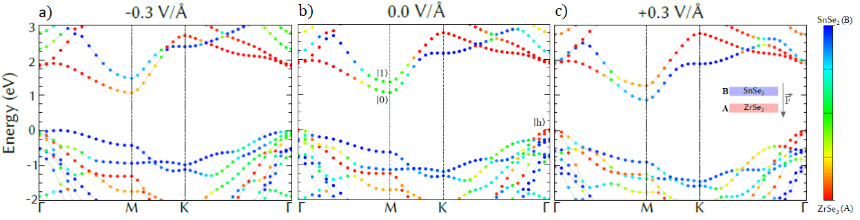 Figure 1
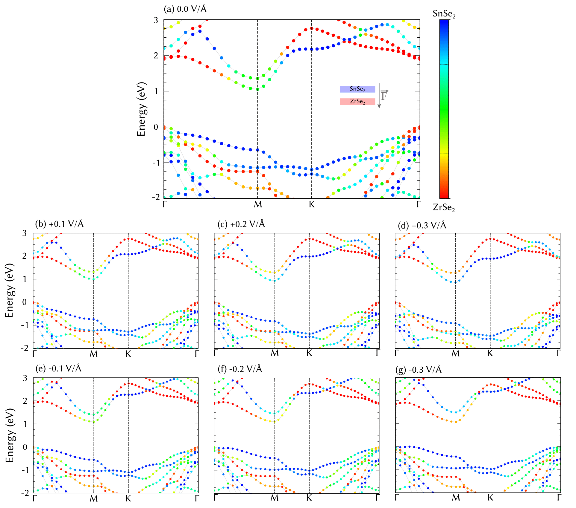 Figure 2
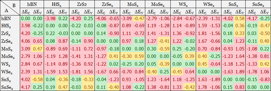 Figure 3
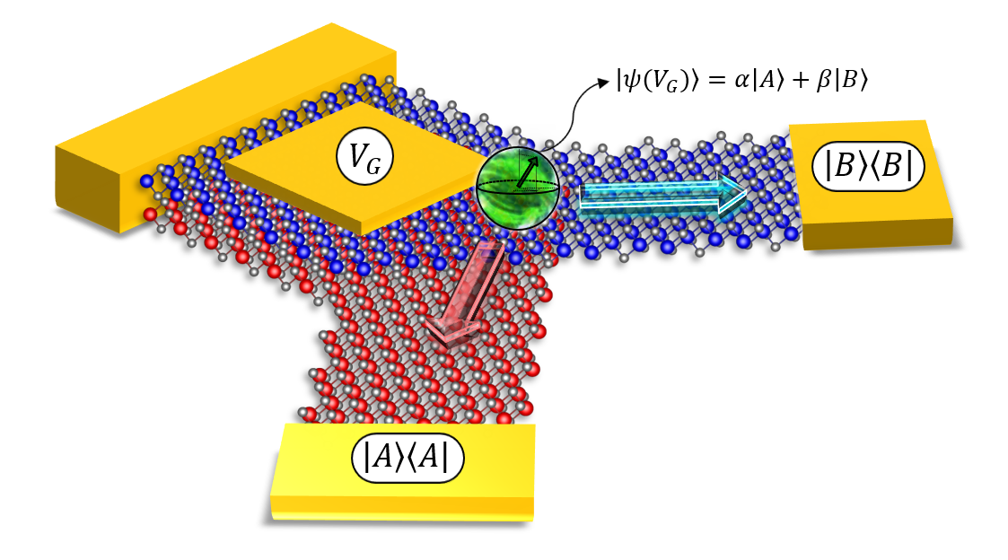 Figure 4
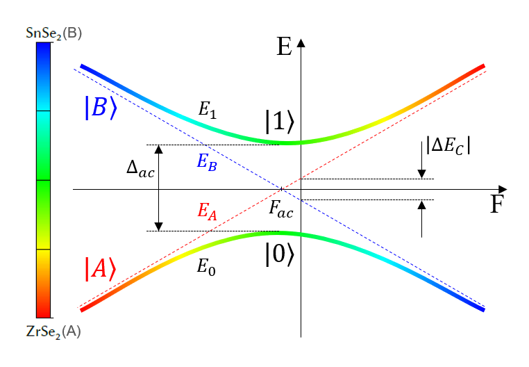 Figure 5
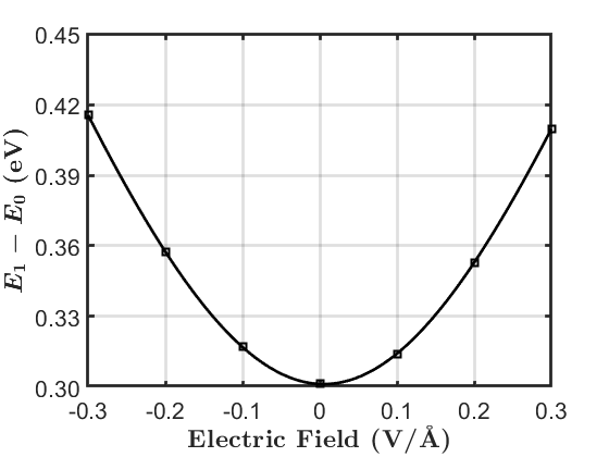 Figure 6
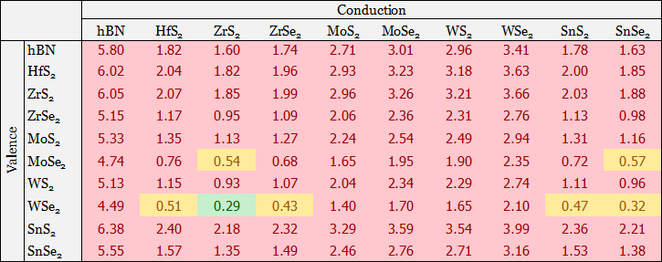 Figure 7
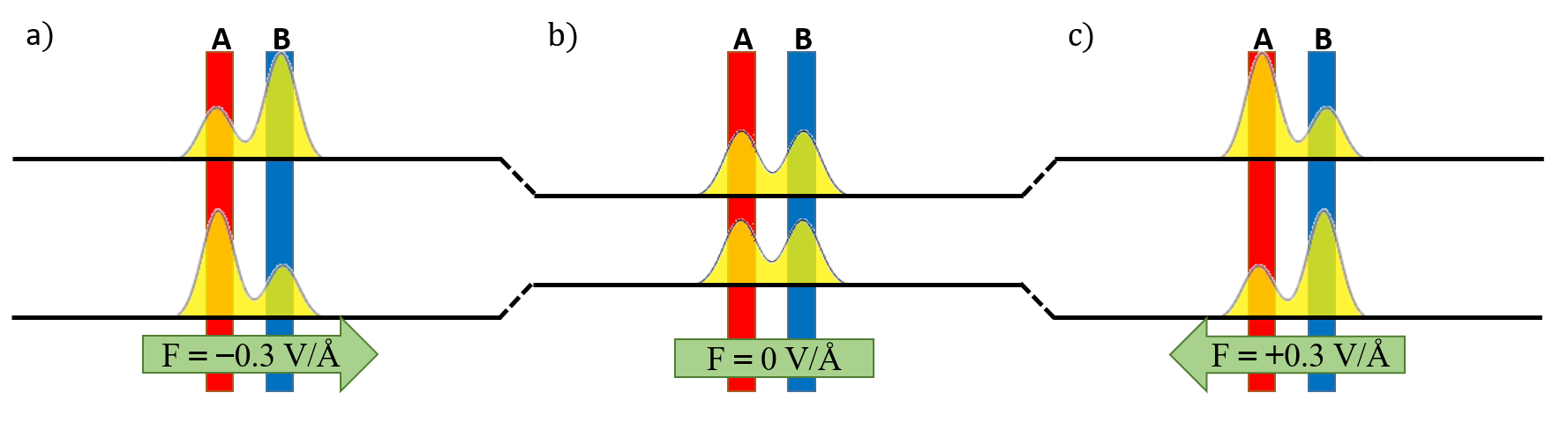 Figure 8
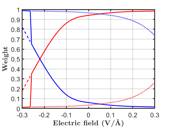 Figure 9
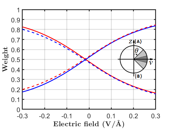 Figure 10
Peer Reviews
No public reviews on file for this paper yet. If you reviewed it on a platform where reviews are public (OpenReview, ICLR, NeurIPS, ICML), you can paste yours below so the community can read it here.
Videos
No videos yet. Explain this paper in a talk, walkthrough, or lecture? Add one.
††thanks: Current address: Department of Materials Science and Engineering, Massachusetts Institute of Technology, Cambridge, MA 02139
Charge qubit in van der Waals heterostructures
Bruno Lucatto
Grupo de Materiais Semicondutores e Nanotecnologia, Instituto Tecnológico de Aeronáutica, DCTA, 12228-900 São José dos Campos, Brazil
Daniel S. Koda
Grupo de Materiais Semicondutores e Nanotecnologia, Instituto Tecnológico de Aeronáutica, DCTA, 12228-900 São José dos Campos, Brazil
Friedhelm Bechstedt
Institut für Festkörpertheorie und -optik, Friedrich-Schiller-Universität, Max-Wien-Platz 1, D-07743 Jena, Germany
Marcelo Marques
Grupo de Materiais Semicondutores e Nanotecnologia, Instituto Tecnológico de Aeronáutica, DCTA, 12228-900 São José dos Campos, Brazil
Lara K. Teles
Grupo de Materiais Semicondutores e Nanotecnologia, Instituto Tecnológico de Aeronáutica, DCTA, 12228-900 São José dos Campos, Brazil
Abstract
The use of spatial quantum superpositions of electron states in a gated vdW heterostructure as a charge qubit is presented. We theoretically demonstrate the concept for the ZrSe2/SnSe2 vdW heterostructure using rigorous ab initio calculations. In the proposed scheme, the quantum state is prepared by applying a vertical electric field, is manipulated by short field pulses, and is measured via electric currents. The qubit is robust, operational at high temperature, and compatible with the current 2D technology. The results open up new avenues for the field of physical implementation of qubits.
††preprint: APS/123-QED
I Introduction
The quantum superposition (QS) principle plays a major role in the so-called second generation of quantum technologies, which includes quantum counterparts of cryptography, imaging, computing, and sensing Georgescu and Nori (2012). Preparation, manipulation, and measurement of the QS are central aspects to enable the operation of such advanced devices. The superposition of two quantum states characterizes the unit of quantum information, a qubit, typically implemented by two-level systemsSchneider and Saenz (2012), polarization of light O’Brien et al. (2003) or electron spin orientationsLaucht et al. (2016).
Solid-state quantum bits are attractive options such as spin qubits with electrically tunable spin-valley mixing in siliconCrippa et al. (2018); Bourdet and Niquet (2018), the qubit of the two charge states of a negatively charged nitrogen vacancy in diamondLucatto et al. (2017); Chou et al. (2018), and the charge-qubit operation of an isolated double quantum dotGorman et al. (2005). All these examples show that atomic-like structures in or of solids may be used as building blocks of future quantum computers or quantum information devices. Recently, along with the strong development of two-dimensional (2D) material technology, progress has been made to find possible candidates for qubits in monolayerPawłowski et al. (2018) and multilayerKhorasani and Koottandavida (2017); Wang et al. (2019) structures.
One striking property of 2D materials is the formation of van der Waals (vdW) heterostructures, which consist of stacks of 2D crystalsGeim and Grigorieva (2013); Novoselov et al. (2016); Liu et al. (2016). Despite the weak interaction between the two atomic layers in such a 2D heterostructure, if the band structures of the isolated sheets are nearly aligned on an absolute energy scale, QS can arise from wavefunctions localized in different layers but forming the conduction or valence bands of the heterostructureKoda et al. (2018). Bonding and antibonding combinations of orbitals localized on each subsystem build the basis functions of the joint conduction or valence bandKoda et al. (2017). The resulting energy splittings and mixing coefficients of the wavefunctions depend on the vdW interlayer distance and the natural band discontinuities Koda et al. (2018). The mixing coefficients characterize the quantum-mechanical probabilities to find a certain carrier, electron or hole, in each of the two 2D materials of the heterostructure. However, despite the fact that the QS property in 2D vdW heterostructures is highly promising, it has not yet been explored for qubit applications.
In this Letter, we propose solid-state qubits based on Bloch states of a 2D vdW heterostructure. In particular, we consider as a benchmark the system ZrSe2/ SnSe2 in which the qubit consists of a QS of the two first conduction states at M point. These states can be manipulated by a vertical electric field oriented in the stacking direction, modifying the band alignments and, consequently, the mixing coefficients. Thereby, the probabilities to measure a certain carrier on a specific side of the heterocombination can be modulated. The time variation of the electric field allows for the control of the individual qubit state. By means of ab initio calculations, we demonstrate the effects of superposition as well as its manipulation via the gate field. An example of a measurement scheme is presented. The proposed system is robust and compatible with the current technology of 2D materials.
II Effect of vertical electric field on band structure
To illustrate the superposition of states for electrons and holes in biased 2D vdW heterostructures, we start with a model system consisting of ZrSe2 and SnSe2 transition metal dichalcogenide monolayers. Because of the near lattice match, 1x1 cells with zero twist and small antisymmetric biaxial strain of 0.8% are chosen Koda et al. (2017). A vertical electric field simulates that the heterostructure is gated or vertically biased as displayed in the inset of Fig. 1c. The band structures resulting for three field strengths are plotted in Fig. 1 along with high-symmetry directions in the Brillouin zone (BZ) for a small energy interval around the fundamental gap. The indirect semiconductor character with the conduction band minimum (CBM) at M and the valence band maximum (VBM) at is conserved for all field strengths. In Fig. 1, the color of each eigenvalue represents the relative contribution of each crystal to the wavefunction. It is obtained as the proportion of the projections of the Kohn-Sham orbitals onto the atomic orbitals (i.e., the orbital character of these levelsLucatto et al. (2017)) for all the atoms in each material. In this work, the two-level system of the qubit is defined as the two lowest conduction states at the M point in the BZ. The lowest conduction band state at M may be denoted by , whereas the next conduction band state is higher in energy by eV but remains at the same point. The hybridization is also present in other states at the band edges, which may impact measures of carrier concentration. In this sense, we also include in the following analysis the hole state in the VBM at , denoted by . These band states are composed by wavefunctions localized at one of the 2D crystals. Figure 1 clearly shows that their contribution can be manipulated by an external field .
In the unbiased case (Fig. 1b), and have almost equal contributions of each layer of the heterojunction as indicated by the green dots. In the absence of an electric field, an electron in one of these states tends to be in an electronic state with equal probabilities to find the carrier in material A or B. Instead, in the biased case, the conduction band states are given by superpositions of the wavefunctions that belong to material A or to material B with different weights as illustrated in Fig. 2. This behavior is different from what happens at the top valence band state. The character of is predominantly from A, as indicated by the red color of the VBM in Fig. 1b. Therefore, a hole tends to be localized in crystal A.
An external electric field in stacking direction of the vdW heterostructure can shift the bands of the crystals with respect to each other, as indicated in Figs. 1a and 1c. The corresponding change in energy also impacts the overlap of the orbitals, thus affecting their relative contribution to the bilayer wave function. By applying an electric field in B-A direction, as indicated by the inset in Fig. 1c, electrons at are lowered in energy. The electric field then shifts down the band structure of material B relatively to the band structure of material A, consequently letting be a state with a stronger character of material B, as indicated by Fig. 1c. As becomes more localized at B, and becomes more localized at A. The consequences for the wave function localization are depicted in Fig. 2c.
The opposite holds true when we apply an electric field in the reverse direction: the bands of material B are shifted toward the vacuum level, allowing to be more localized at A and more localized at B, as indicated in Figs. 1a, and 2a. However, this is not the only effect observed in this case. Since the band structure of material B is shifted toward higher absolute energies, the VBM of material B starts to line up with the VBM of material A, and thus exhibits a stronger hybridization and nearly equal contributions from both sheets A and B, as indicated by the colors of Fig. 1a. Moreover, for this extreme field situation, the VBM is slightly shifted from , which is not true for the intermediate values (see the Supporting Information for a more detailed discussion on hole states).
There is a complementarity between and under the influence of the gate field, where one state becomes more localized in one sheet as the other becomes more localized in the other sheet. Therefore, an electron occupying any superposition of the two states localized in different sheets configures a charge qubit in the AB heterostructure, where for strong positive electric fields the and states are localized in sheets B and A, respectively, and the opposite happens for strong negative electric fields. The corresponding energy configuration is illustrated schematically in Fig. 3 as a function of the electric field. An anticrossing energy eV is determined by the difference between the eigenenergies and of the band states and , respectively, for an electric field, where the layer contributions are equal. This energy difference corresponds to a frequency THz. In the studied system, this occurs at nearly vanishing field mV/Å, as depicted in Figs. 3 and 4. The conduction-level system, therefore, has similarities with the electronic structure of the charge qubit suggested in a double quantum dot Gorman et al. (2005).
The contribution of each layer A or B to the Bloch wave function of the states and in the AB heterostructure strongly depends on the electric field strength . Thus, an electron wave function of the AB heterostructure is mainly a combination of the corresponding wave functions and of the two individual atomic sheets with different weights. It can be written as a superposition for a given field strength
[TABLE]
with complex coefficients. Because of the relatively large distance between the sheets, we consider the overlap of these states to be small, such that the normalization of the coefficients is given by . Under this approximation, and are orthogonal and, therefore, the squared moduli of their coefficients give the weights of each sheet to the wavefunction, as illustrated in Fig. 4. This figure also provides evidence for the complementarity between and , which further justifies the usage of the system as a charge qubit realized in the sheet arrangement.
The representation (1) can be also interpreted as a coherent superposition of basic quantum states and at a given time or field strength, where the probability amplitudes , to find an electron characterize a linear combination as in a single qubit Schumacher (1995). In a linear approximation around the state of maximum delocalization, considering , one finds for the biased ZrSe2/SnSe2 heterostructure
[TABLE]
The states of Eq. (1) can be described as a Bloch vector in the standard Bloch sphere representation, where the mixing coefficients are described by spherical coordinates with angles and as
[TABLE]
The polar angle can be calculated as
[TABLE]
For the considered values of the electric field, the Bloch vector lies in the shaded area depicted in the inset of Fig. 4, which corresponds to the interval between and . Considering V/Å, the linear approximation introduces a small error, and the vector lies in the dark gray area in the inset of Fig. 4.
III Usage as qubit
A general superposition state on the described two-level system for a given field can be expanded in the energy eigenvector basis as . Writing the energy eigenvectors in the A/B basis, and , we find that in this basis is written as , where
[TABLE]
A possible application of the two-level system as a quantum bit is to initialize the system in the desired state, by choosing a suitable electric field strength and allowing the system to relax to ensure the electron is in the lowest CBM, i.e., in state . In order to apply single-qubit gate operations, the gate field is set to another value, thus changing the two-level system’s Hamiltonian itself, since it is a function of the field strength . If this change is made within a slow process, the coefficients of the energy eigenvectors basis and would stay constant throughout the process, under the conditions of the adiabatic theorem. Therefore, the electron would stay in state , regardless of the wavefunction of being different from the starting one, which implies that and are changed. On the other hand, if the variation of the electric field is fast enough, the electron wavefunction would be approximately unchanged during the whole process, i.e., and would be constant. Together with the fact that the coefficients of the energy eigenstates in the A/B basis change with the electric field, this implies that and change. This behavior opens the possibility of moving the electron to the excited state without recurring to optical excitations. In order to measure the resulting state, the carrier concentrations in each sheet must be measured in a time window and compared to each other.
An example of operation would be to setup the system with a strong negative field, i.e., to start with and , then suddenly change the electric field to a strong positive one. Presuming the field switch happens fast enough, the electron state remains the same, i.e., or . However, after the switching, these site states correspond to the opposite energy eigenstates of the Hamiltonian for the new field strength, i.e., and . Therefore, by doing so, a Pauli-X quantum gate is applied to the qubit. By applying an additional external bias in the horizontal direction in each sheet, a small carrier drift can be induced, and by measuring the resulting currents the carrier concentration in the layers can be deduced. A possible structure for the device that would allow for the operations here described is depicted in Fig. 5.
Since the variation of the orbital character of a band is continuous with respect to the crystal momentum (see Fig. 1), even if more than one electron is excited, we can assume that it will have approximately the same mixing coefficients as the first one. The Pauli exclusion principle is satisfied due to the difference in the crystal momentum quantum number. Therefore, it may be possible to perform the same operation with many electrons at the same time, if the decoherence time does not decrease too much due to carrier collisions. This would allow for single measurement operation, since the desired statistics of the results would be given by the relative amplitude between the currents flowing through each sheet. Experimental realization of the qubit should provide a measure of how the (electro)chemical potential position affects the decoherence time. Besides, since , where is the Boltzmann constant and is the room temperature, we expect the system to operate at room temperatures.
It is worth emphasizing that the described vdW charge qubit is not restricted to the studied system. Instead, due to the fact that there are several possible combinations of 2D materials, it is highly probable that other similar systems exist. Considering that there is a practical limit to the intensity of electric fields that can be applied, which also limits how much bands can be shifted with respect to each other, a first filter to predict vdW combinations that may present QS is by analyzing their natural band alignments, as shown in Tables S1 and S2 of the Supporting Information. However, for a real prediction, one needs to go further and make electronic structure calculations, since the desired hybridization effect depends not only on the proximity of the energy levels Koda et al. (2018). Moreover, applying strain on the heterostructure may also lead to hybridization in systems with large natural band discontinuities Koda et al. (2017).
IV Computational Details
The structural and electronic properties are calculated using the density functional theory (DFT) as implemented in the Vienna Ab-initio Simulation Package (VASP) Kresse and Furthmüller (1996). The wave functions and pseudopotentials are generated within the projector-augmented wave (PAW) method Kresse and Joubert (1999). Exchange and correlation (XC) are described using the Perdew-Burke-Ernzerhof (PBE) functional within the generalized gradient approximation (GGA) Perdew et al. (1996). Van der Waals interaction is taken into account using the optB86b functional Klime et al. (2011). The repeated slab method is applied to simulate individual 2D crystals as well as their heterocombinations Bechstedt (2003). Minimum lateral unit cells employed are found within the coincidence lattice method Koda et al. (2016). To account for the excitation aspect we add approximate quasiparticle corrections to the Kohn-Sham bands by applying the XC hybrid functional HSE06 Paier et al. (2006); Heyd et al. (2003, 2006). More detailed information is given in the Supporting Information.
V Conclusion
In summary, we identified the existence of spatial quantum superposition states in the conduction bands of van der Waals heterostructures with small natural band discontinuities and proposed their gate-field manipulation that can be employed in device applications. Explicitly, we performed rigorous ab initio calculations for the model vdW heterostructure consisting of atomic sheets of ZrSe2 and SnSe2 on which a variable vertical electric field was applied. We obtained quantitative conduction band structures which demonstrate the feasibility of controlling the probability of the electron being on a specific side of the heterostructure by the external field. Finally, we proposed to use the system as a charge qubit, which is based in a robust electronic state, does not require cryogenic operating temperatures, and is compatible with the preparation technology of 2D electronic devices.
Acknowledgements.
The authors thank Dr. Ivan Guilhon for the fruitful discussions and revision of the text. This work was funded by the Brazilian agencies FAPESP (grant n. 2012/50738-3), CAPES (PVE - grant n. 88887.116535/2016-00), and CNPq (grants n. 305405/2014-4, 308742/2016-8, and 154636/2016-9). We acknowledge the National Laboratory for Scientific Computing (LNCC/MCTI, Brazil) for providing HPC resources of the SDumont supercomputer.
The reference list from the paper itself. Each links out to its DOI / PubMed record.
- 1Georgescu and Nori (2012) I. Georgescu and F. Nori, “Quantum technologies: An old new story,” Physics World 25 , 16–17 (2012).
- 2Schneider and Saenz (2012) P. I. Schneider and A. Saenz, “Quantum computation with ultracold atoms in a driven optical lattice,” Physical Review A 85 , 1–5 (2012).
- 3O’Brien et al. (2003) J. L. O’Brien, G. J. Pryde, A. G. White, T. C. Ralph, and D. Branning, “Demonstration of an all-optical quantum controlled-NOT gate,” Nature 426 , 264–267 (2003).
- 4Laucht et al. (2016) A. Laucht, R. Kalra, S. Simmons, J. P. Dehollain, J. T. Muhonen, F. A. Mohiyaddin, S. Freer, F. E. Hudson, K. M. Itoh, D. N. Jamieson, J. C. Mc Callum, A. S. Dzurak, and A. Morello, “A dressed spin qubit in silicon,” Nature Nanotechnology 12 , 61–66 (2016).
- 5Crippa et al. (2018) A. Crippa, R. Maurand, L. Bourdet, D. Kotekar-Patil, A. Amisse, X. Jehl, M. Sanquer, R. Laviéville, H. Bohuslavskyi, L. Hutin, S. Barraud, M. Vinet, Y. M. Niquet, and S. De Franceschi, “Electrical Spin Driving by g -Matrix Modulation in Spin-Orbit Qubits,” Physical Review Letters 120 , 1–5 (2018).
- 6Bourdet and Niquet (2018) L. Bourdet and Y. M. Niquet, “All-electrical manipulation of silicon spin qubits with tunable spin-valley mixing,” Physical Review B 97 , 1–9 (2018).
- 7Lucatto et al. (2017) B. Lucatto, L. V. C. Assali, R. R. Pela, M. Marques, and L. K. Teles, “General procedure for the calculation of accurate defect excitation energies from DFT-1/2 band structures: The case of the NV - center in diamond,” Physical Review B 96 , 075145 (2017).
- 8Chou et al. (2018) J. P. Chou, Z. Bodrog, and A. Gali, “First-Principles Study of Charge Diffusion between Proximate Solid-State Qubits and Its Implications on Sensor Applications,” Physical Review Letters 120 , 136401 (2018) .