Waveguide-integrated van der Waals heterostructure photodetector at telecom band with high speed and high responsivity
Nikolaus Fl\"ory, Ping Ma, Yannick Salamin, Alexandros Emboras,, Takashi Taniguchi, Kenji Watanabe, Juerg Leuthold, Lukas Novotny

TL;DR
This paper demonstrates a high-speed, high-responsivity photodetector using van der Waals heterostructures integrated on silicon photonics, achieving record bandwidths up to 50GHz at telecom wavelengths.
Contribution
It introduces a vertical MoTe2/graphene heterostructure design that minimizes carrier transit time, enabling record-high bandwidths in integrated 2D material-based photodetectors.
Findings
Bandwidth of at least 24GHz at -3V bias
Bandwidth boosted to 50GHz with higher bias or thinner flakes
Responsivity of 0.2A/W at 1300nm
Abstract
Intensive efforts have been devoted to exploit novel optoelectronic devices based on two-dimensional (2D) transition-metal dichalcogenides (TMDCs) owing to their strong light-matter interaction and distinctive material properties. In particular, photodetectors featuring both high-speed and high-responsivity performance are of great interest for a vast number of applications such as high-data-rate interconnects operated at standardized telecom wavelengths. Yet, the intrinsically small carrier mobilities of TMDCs become a bottleneck for high-speed application use. Here, we present high-performance vertical van der Waals heterostructure-based photodetectors integrated on a silicon photonics platform. Our vertical MoTe2/graphene heterostructure design minimizes the carrier transit path length in TMDCs and enables a record-high measured bandwidth of at least 24GHz under a moderate bias…
Click any figure to enlarge with its caption.
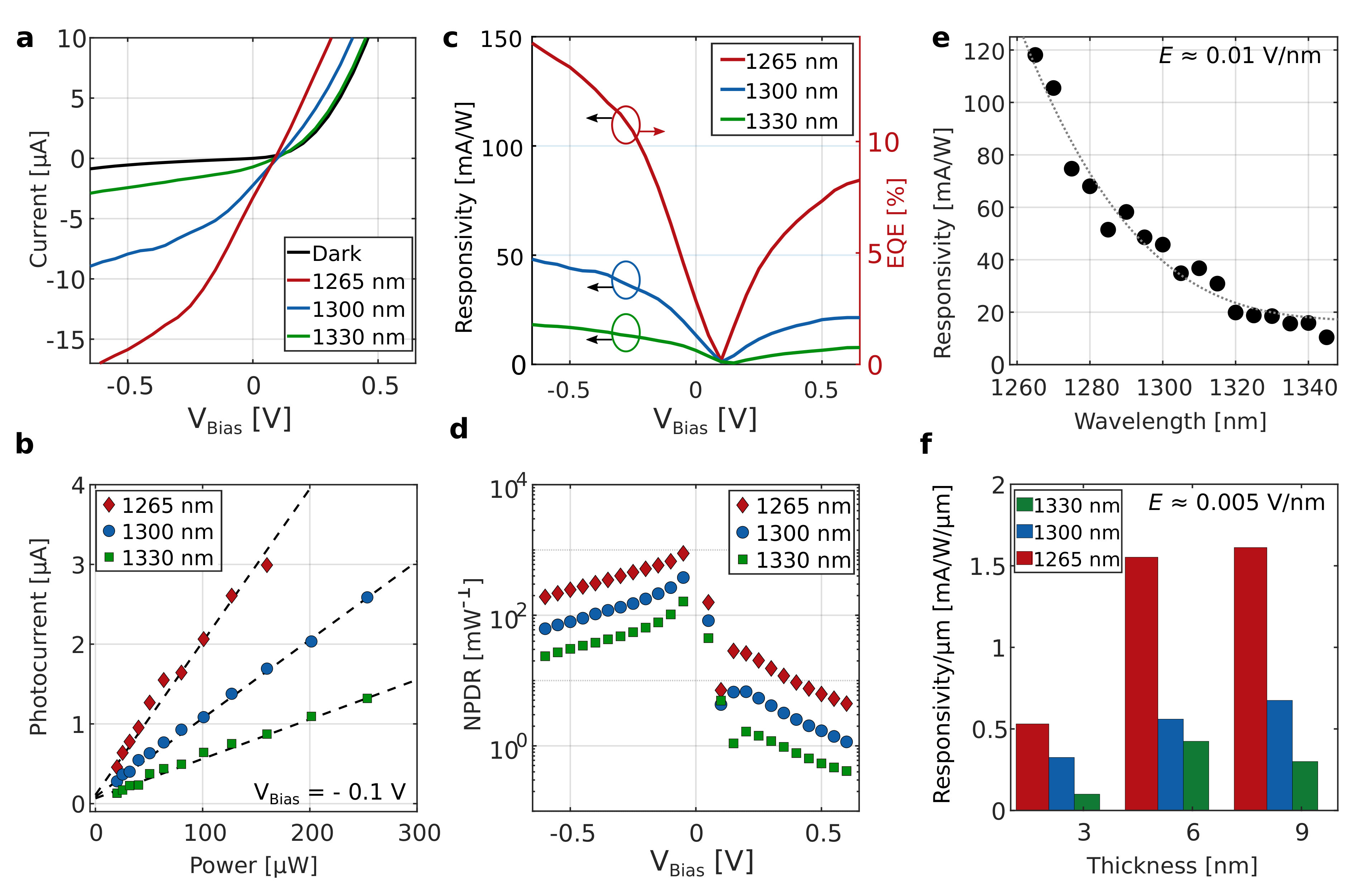 Figure 3
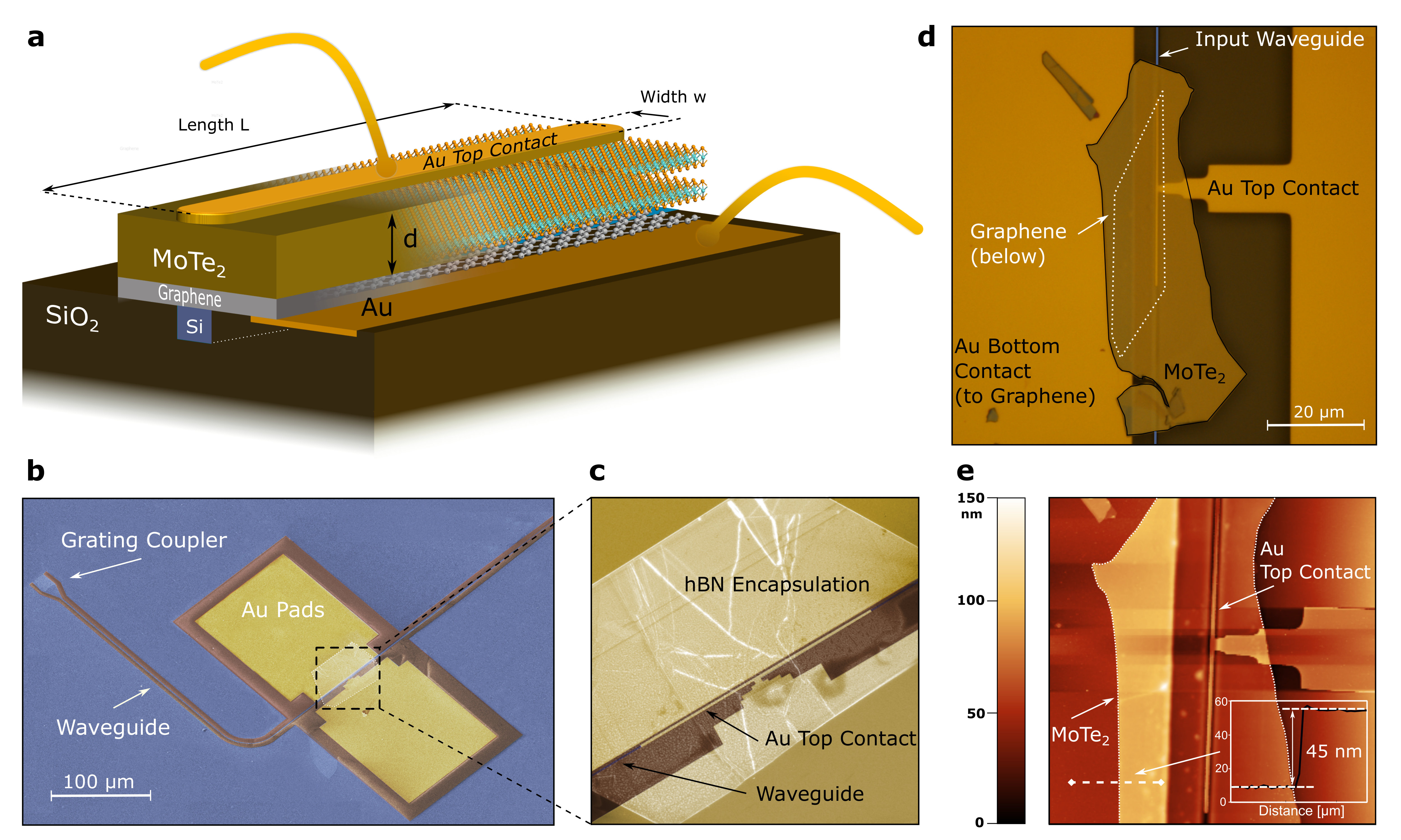 Figure 1
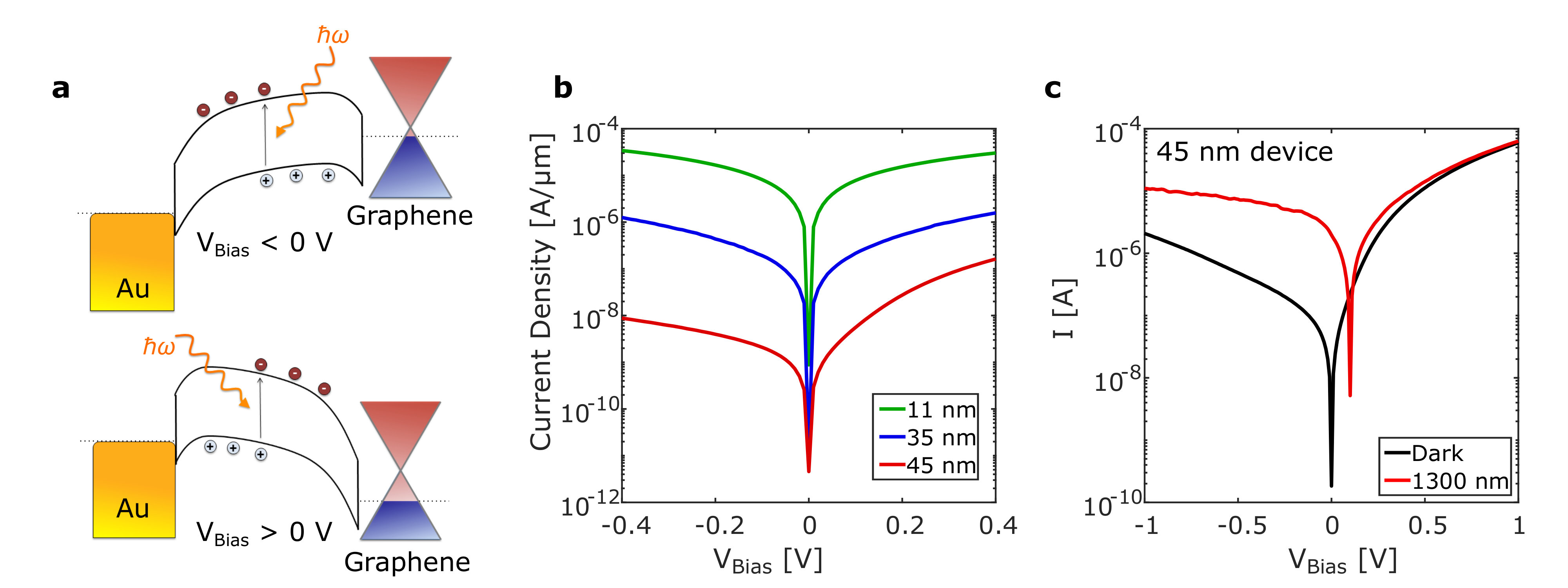 Figure 2
 Figure 3
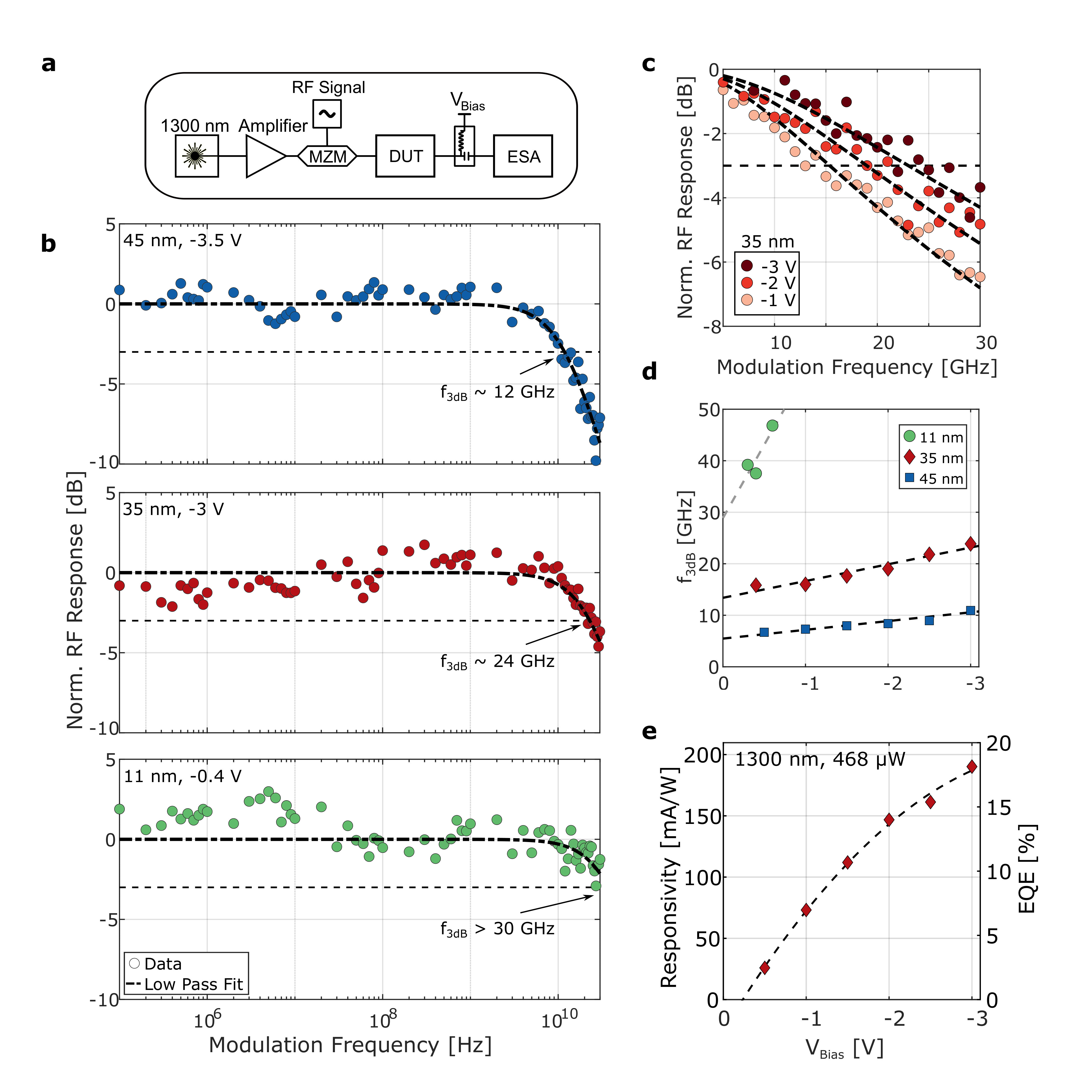 Figure 4
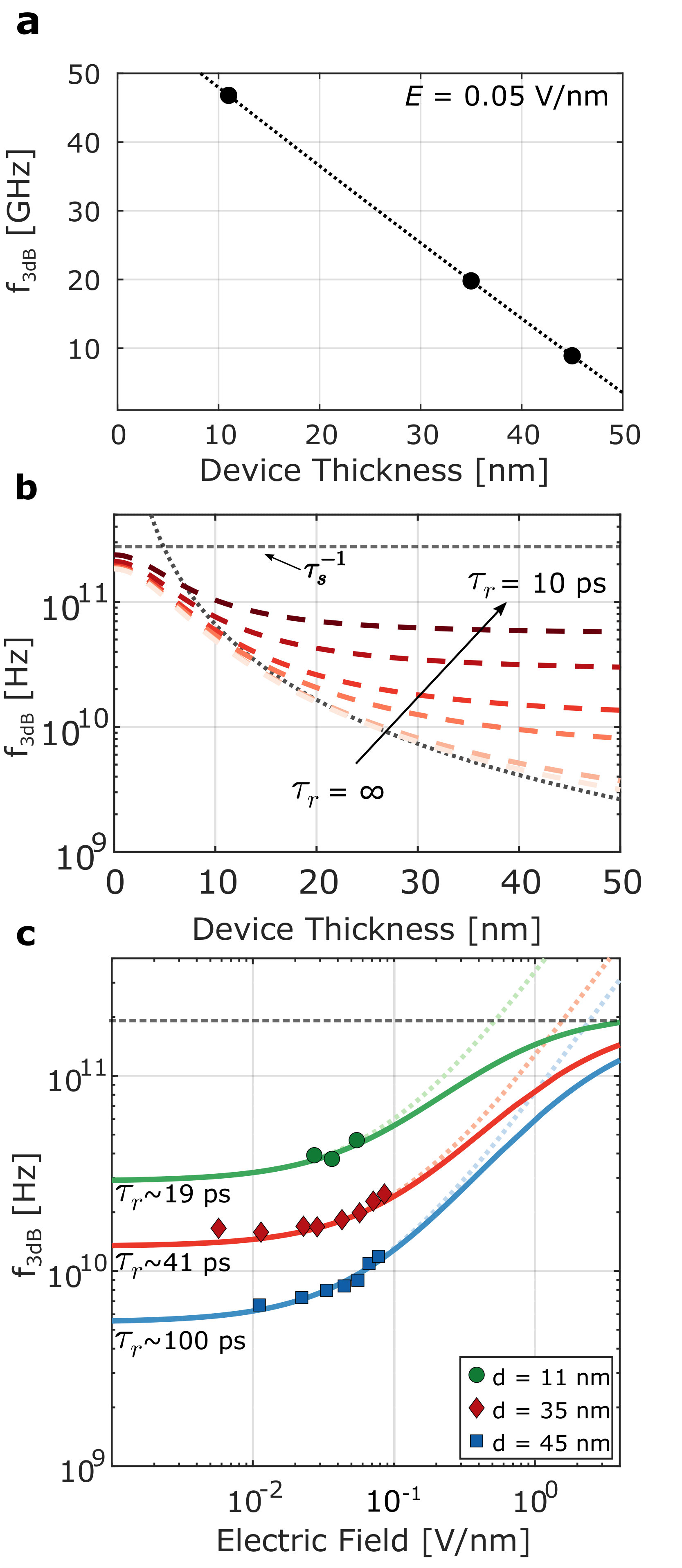 Figure 5
Peer Reviews
No public reviews on file for this paper yet. If you reviewed it on a platform where reviews are public (OpenReview, ICLR, NeurIPS, ICML), you can paste yours below so the community can read it here.
Videos
No videos yet. Explain this paper in a talk, walkthrough, or lecture? Add one.
††thanks: These authors contributed equally.††thanks: These authors contributed equally.
Waveguide-integrated van der Waals heterostructure photodetector at telecom band with high speed and high responsivity
Nikolaus Flöry
Photonics Laboratory, ETH Zürich, 8093 Zürich, Switzerland
Ping Ma
Institute of Electromagnetic Fields, ETH Zürich, 8092 Zürich, Switzerland
Yannick Salamin
Institute of Electromagnetic Fields, ETH Zürich, 8092 Zürich, Switzerland
Alexandros Emboras
Institute of Electromagnetic Fields, ETH Zürich, 8092 Zürich, Switzerland
Takashi Taniguchi
National Institute for Material Science, 1-1 Namiki, Tsukuba 305-0044, Japan
Kenji Watanabe
National Institute for Material Science, 1-1 Namiki, Tsukuba 305-0044, Japan
Juerg Leuthold
Institute of Electromagnetic Fields, ETH Zürich, 8092 Zürich, Switzerland
Lukas Novotny
Photonics Laboratory, ETH Zürich, 8093 Zürich, Switzerland
[email protected], [email protected], [email protected]
††preprint:
**Intensive efforts have been devoted to exploit novel optoelectronic devices based on two-dimensional (2D) transition-metal dichalcogenides (TMDCs) owing to their strong light-matter interaction and distinctive material properties Wang2012 ; Xiao2017 . In particular, photodetectors featuring both high-speed and high-responsivity performance are of great interest for a vast number of applications such as high-data-rate interconnects operated at standardized telecom wavelengths Koppens2014a ; Ferrari2018 . Yet, the intrinsically small carrier mobilities of TMDCs become a bottleneck for high-speed application use Konstantatos2018 . Here, we present high-performance vertical van der Waals heterostructure-based photodetectors integrated on a silicon photonics platform. Our vertical MoTe2/graphene heterostructure design minimizes the carrier transit path length in TMDCs and enables a record-high measured bandwidth of at least 24 GHz under a moderate bias voltage of 3 volts. Applying a higher bias or employing thinner MoTe2 flakes boosts the bandwidth even to 50 GHz. Simultaneously, our device reaches a high external responsivity of 0.2 A/W for incident light at 1300 nm, benefiting from the integrated waveguide design. Our studies shed light on performance trade-offs and present design guidelines for fast and efficient devices. The combination of 2D heterostructures and integrated guided-wave nano photonics defines an attractive platform to realize high-performance optoelectronic devices Mueller2015 ; Liu2016f ; Yu2013e , such as photodetectors Britnell2013b , light-emitting devices Withers2015 and electro-optic modulators Sun2016b .
**
During the last decade, two-dimensional (2D) materials such as graphene and transition-metal dichalcogenides (TMDCs) have shown great promise for a wide range of photonic and optoelectronic applications Bonaccorso2010a ; Boltasseva2019 ; Manzeli2017 . 2D devices have the potential to outperform established and more mature technologies, particularly in terms of form factor, operating conditions and cost-effectiveness. The possibility to integrate 2D materials without constraints of crystal lattice matching is disruptive, as it tremendously simplifies manufacturing and increases possible material combinations. Graphene, which has been widely used for successful 2D device implementations Kim2011 ; Schuler2018 ; Phare2015 ; Gan2013d ; Hone2015 ; Ma2019 , has an intrinsically weak photosensitivity, though its interaction with light can be enhanced using silicon-based integrated photonics, such as optical resonators Phare2015 or waveguides Youngblood2016a . Nevertheless, graphene-based devices suffer from other issues stemming from its gapless nature, e.g., large dark currents for photodetectors. Alternatively, TMDCs, a semiconducting class of 2D materials, hold great promise for high-performance optoelectronic devices due to their intrinsically strong light-matter interactions Mak2016a . Yet, the integration with a silicon-based platform is challenging, because direct band-to-band transition energies of TMDCs fall within the absorption band of silicon. Despite of this, few attempts have been made towards the integration of TMDCs with silicon-based structures Bie2017 ; Ma2018a , but high-performance devices, especially operated at standardized telecom bands relevant for applications of information and communication technology (ICT) Ferrari2018 , are still under very limited investigation.
Another major challenge of employing TMDCs for ICT devices is the speed performance. This is of particular importance when TMDCs are employed in photodetectors Koppens2014a ; Konstantatos2018 ; Buscema2015 . While impressive photoresponsivities and photoconductive gains have been demonstrated Lopez-Sanchez2013a ; Yu2017 , what is easily overseen is that these high gains typically originate from photogating effects Konstantatos2018 ; Lopez-Sanchez2013a . The associated long carrier lifetimes inherently limit the speed performance Konstantatos2018 ; Wang2016h . Moreover, the carrier mobilities of TMDCs are significantly smaller than those of graphene Ma2018a ; Octon2016c , which poses an obstacle for high-speed device performance. To date, the highest reported bandwidth of TMDC waveguide detectors is below 1 GHz Bie2017 ; Ma2018a , limited by the relatively long transit time of carriers before they are collected. It is therefore highly desirable to investigate TMDC device configurations for an improved speed performance, e.g. comparable to graphene-based devices, but with higher efficiency.
In this Letter we present high-speed and high-responsivity vertical MoTe2/graphene van der Waals heterostructure photodetectors integrated with planar silicon photonic waveguides to address the aforementioned key technology challenges. The device design takes full advantage of van der Waals heterostructures as well as of the waveguide integration scheme. Both of these are essential to overcome the intrinsic material constraints and allow us to demonstrate application-level device performance of up to 50 GHz bandwidth and photoresponsivities of more than 0.2 A/W with low dark currents at the telecom band.
Figure 1a illustrates the concept of the presented photodetector design. A thin flake of semiconducting few-layer MoTe2 is introduced as the light absorbing medium. MoTe2 is compatible with silicon integrated photonics, since it exhibits a layer-dependent bandgap and strong light absorption extending into the standard telecom O-band wavelength range (1260-1360 nm) Ma2018a ; Ruppert2014 . The MoTe2 flake is vertically sandwiched between two parallel electrodes in order to build up a vertical carrier drift path of short distance. The device is operated with transverse electric (TE) polarized light, which has its dominant electric field component parallel to the plane of the MoTe2 flake so as to be efficiently absorbed via band-to-band transitions. Light propagating in the silicon waveguide overlaps evanescently with the absorbing MoTe2 in the active section of the detector. Electron-hole pairs generated by the absorbed photons are efficiently separated and extracted by the uniform electric field applied between the bottom and top electrodes.
The high speed of the device is a result of several factors. First, the use of a vertical heterostructure remedies the low mobility of TMDCs. The bandwidth () of a transit-time-limited device is where is the carrier transit time, the carrier velocity and the length of the carrier transit path Kato1993 ; Xia2009b ; Massicotte2015c . In previously reported TMDC waveguide detectors, the photo-excited carriers were transported in-plane over much longer distances by lateral electric fields Bie2017 ; Ma2018a ; Youngblood2015 . A vertical heterostructure on the other hand enables a vertical channel that restricts the transit path length of photoexcited carriers down to a few nanometers, thereby achieving much smaller transit times. Second, monolayer graphene is adopted as a transparent bottom electrode. On one hand, it allows the optical mode to spatially overlap with the MoTe2 absorber and, on the other hand, the high conductivity and carrier mobility of graphene ensures fast carrier extraction and small series resistance. Third, a narrow metallic contact made of thin-film gold (Au) on top of MoTe2, is aligned along the integrated waveguide and results in a small but well-defined vertical carrier extraction channel overlapping with the guided optical mode. The use of such a shaped top electrode allows the active area of the device to be very small, which minimizes the circuital capacitance of the device. Together with the small circuital resistance, this results in a large resistance-capacitance (RC)-limited bandwidth. Besides, the asymmetric contact scheme generates a built-in electric field that contributes to the carrier separation under zero and low bias conditions.
It is noteworthy that by design the light absorption and detection of the presented devices are scalable with the length of the integrated waveguide, while the collection path of photogenerated carriers is perpendicular to the light propagation direction. As a result, our device has no trade-offs between the carrier transit-time limited bandwidth and quantum efficiency. This is different for surface-normal illuminated photodetectors, for which the length of the absorber is finite and light absorption is low. The waveguide integration approach in our device is crucial for achieving high-speed performance while maintaining a high responsivity.
The fabrication of our devices is detailed in the Methods and Supplementary Section S1. In short, buried silicon waveguides were first fabricated on standard silicon-on-insulator wafers by using a LOCal Oxidation of Silicon (LOCOS) technique Desiatov2010 ; Naiman2015a . Grating couplers (GCs) were produced by shallow etching of silicon. Flakes of MoTe2 with various thicknesses and monolayer graphene were obtained by means of mechanical exfoliation and stacked employing a polymer-based pick-up technique Britnell2013b ; Zomer2014a . The stacked MoTe2-graphene heterostructures were subsequently transferred to the silicon photonics chips and aligned to the buried waveguides. After transfer of the 2D flakes, a top metallic contact was patterned onto the MoTe2 by electron-beam lithography (EBL), metal evaporation and a lift-off process. Figure 1b displays a scanning electron microscope (SEM) image of a fabricated device, including the access silicon waveguide, the GC, and the detector structure as shown in Fig. 1c with an enlarged view. Figure 1d and 1e show a top-view optical microscope image and an atomic force microscope (AFM) image of a fabricated detector before final device encapsulation by a large flake of hexagonal boron nitride (hBN). Cross-sectional AFM inspection verifies the thickness of each exfoliated flake of MoTe2 and graphene used in the devices.
Electrical Characteristics. The electrical behavior of the fabricated devices was characterized using a pico-ampere precision source to apply biases and read out the current. The metallic contact pads connected to the bottom graphene electrodes were biased either positively or negatively, while the top contact was grounded. Figure 2a illustrates the band diagram of the studied heterostructure under positive and negative bias conditions, respectively. Both MoTe2 and graphene are known to be lightly p-doped Lee2008a . The Fermi level of Au is aligned and pinned close to the valence band of MoTe2 Shin2017a ; Nakaharai2016 ; Wee2017a . This pinning tends to remain unchanged regardless of the thicknesses of TDMC flakes Shin2017a . Graphene on the other hand forms a smaller and tunable Schottky barrier after contacting MoTe2 Wang2016h ; Yu2017 . The difference in work function of Au and graphene leads to a built-in potential in the device. Applying a bias voltage increases the potential drop across the device that drives the photo-excited carriers. Figure 2b shows the current density against the applied bias voltage for devices comprising flakes of three different MoTe2 thicknesses and lengths, more exactly, 11 nm and 20 m, 35 nm and 33 m, and 45 nm and 40 m. The measured current is normalized to the effective detector length of each device to account for the size-variations of the used flakes. As expected, the highest current density can be observed for the thinnest device, as a result of the short resistive MoTe2 channel. Moreover, asymmetric current densities under positive and negative bias conditions, induced by the asymmetric contacting scheme, are visible and more pronounced for thicker devices, most likely originating from a MoTe2 thickness-dependent Schottky barrier height between graphene and MoTe2, as previously studied and reported in graphene-TMDC heterostructures Yu2013e ; Wang2016h . This asymmetric contacting scheme also manifests itself in a pronounced photoresponse at zero bias (VBias = 0 V) resulting from an intrinsic built-in field. Figure 2c shows current-voltage (I-V) curves of the 45 nm thick device with and without 1300 nm light coupled into the waveguide. Without any applied voltage the device is already capable to efficiently separate photo-excited electron-hole pairs and to generate a considerable photocurrent of 2 A for 150 W input power, with negligible dark current.
Steady-state photoresponse. The steady-state photoresponse of the fabricated devices was evaluated using linearly TE-polarized laser light with center wavelength of 1300 nm coupled into the integrated waveguides via GCs. The coupling loss of a GC was verified to be around 7.5 dB with the help of nearby reference structures featuring identical waveguide and GC designs fabricated on the same chip, but without detector structures (see Supplementary Section S2 for details). Figure 3a shows I-V measurements with and without light coupled into a device with a 45 nm thick MoTe2 flake. Unless otherwise specified, all data presented in Fig. 3 are based on this specific device. A pronounced increase in current, especially under negative bias voltages, is measured when light is coupled in. The power dependence of this photocurrent is shown in Fig. 3b for different wavelengths. A linear dependence is observed within the measured power range. The photoresponsivity is extracted as the ratio of the photocurrent and the incident optical power delivered to the photodetector. It increases with the applied bias voltage that assists the extraction of carriers. Increasing the applied bias to moderate values of up to 0.6 V, as shown in Fig. 3c, yields photoresponsivities of 150 mA/W, 50 mA/W and 20 mA/W for wavelengths of 1265 nm, 1300 nm and 1330 nm, respectively. This corresponds to an external quantum efficiency (EQE) of 14% at 1265 nm (, denoting the responsivity, the reduced Planck constant, the light angular frequency, and the elementary charge). We intentionally keep the bias voltage low in steady-state photodetection measurements in order not to damage the devices. In fact, the photocurrent and the EQE are expected to further increase for larger applied bias voltages, limited only by break down and saturation of absorption (see Supplementary Section S3 for details on the limits of the responsivity).
Normalized photo-dark-current ratio (NPDR) Goykhman2016 is another important performance indicator of a photodetector. As shown in Fig. 3d, the NPDR of our devices is in the order of 100 mW*-1* under negative bias conditions and approaches 1000 mW*-1* for shorter wavelengths and small bias voltages. This performance outperforms graphene-based photodetectors Gan2013c ; Mueller2010a by order(s) of magnitude. We further characterized the dependence of the photoresponse on the wavelength of the incoupled light. As shown in Fig. 3e, the measured responsivity spectrum agrees with the wavelength dependent absorption of the few-layer MoTe2 flake. It exhibits stronger absorption and hence higher photoresponse for shorter wavelengths.
In Fig. 3f we compare devices with different MoTe2 thicknesses. The figure shows the responsivities, normalized to device length, for light with wavelengths of 1265 nm, 1300 nm and 1330 nm. The observed trend clearly shows that devices consisting of thicker MoTe2 flakes possess a higher photoresponse, which is due to the higher absorption in the thicker semiconducting channel. The behaviour for 1265 nm (red bars) is the same as for 1300 nm (blue bars) and 1330 nm (green bars), despite the overall lower responsivity. These characteristics verify that the observed photoresponse stems from photo-excited carriers generated by light absorption in the semiconducting MoTe2. Although the bottom graphene contact may also contribute to the photocurrent via photo-thermionic effects, the observed linear power dependence as well as the wavelength dependent photocurrent in our devices is in stark contrast to the characteristic features of the photo-thermionic effect Massicotte2016b (i.e. superlinear power behavior and wavelength independent photocurrent). We therefore conclude that in the investigated wavelength range the photo-thermionic contribution of graphene is not significant.
High-frequency photoresponse. To characterize the speed performance of the devices we used the experimental setup illustrated in Fig. 4a. An optical intensity Mach-Zehnder modulator (MZM, u2t MZMO2120) with 30 GHz electro-optic bandwidth was driven by a radio frequency (RF) signal from an electrical synthesizer and used to modulate an amplified continuous-wave laser tunable around 1300 nm. The modulated laser light was coupled into the device via GCs. A bias-tee was used to apply a direct current (DC) bias to the devices. The generated RF electrical signals were extracted from the devices with a high-speed microwave probe and measured with an electrical spectrum analyzer (ESA). The frequency responses ranging from 100 kHz to 30 GHz were measured under various bias voltages. The whole measurement setup was calibrated using a commercially available high-speed photodetector with a bandwidth of 72 GHz (u2t XPDV3120R). Figure 4b shows the measured frequency response of three photodetector devices with different MoTe2 flake thicknesses. In all three cases the response stays flat from 100 kHz to GHz frequencies and then drop off. A standard low pass filter model was used to fit the data, revealing the 3 dB roll-off frequency of each measurement. It is evident from Fig. 4b that devices with thinner MoTe2 exhibit a faster photoresponse. For the 45 nm and 35 nm thick devices we measure a roll-off frequency of 12 GHz at 3.5 V and 24 GHz at 3 V bias, respectively. Whereas the bandwidth of the 11 nm thick MoTe2 device exceeds 30 GHz already at a low bias of 0.4 V, which is beyond the bandwidth of the instruments used in the experiment. The extrapolated 3 dB roll-off frequency is nearly 50 GHz. To the best of our knowledge, this is the highest reported bandwidth of a TMDC-based photodetector, outperforming those of previous studies by more than one order of magnitude Bie2017 ; Ma2018a . For the 35 nm thick MoTe2 device we show in Fig. 4c the influence of the bias voltage on the frequency response in the roll-off regime. The 3 dB roll-off frequency increases with the applied bias since photo-excited carriers are separated faster by large electric fields. Figure 4d plots the roll-off frequencies as a function of the bias voltage for all three devices. It reveals that the bandwidth increases monotonously with bias voltage. This is because the velocity of the carriers increases linearly with applied bias. Furthermore, a high bias not only increases the bandwidth but also leads to an enhanced photoresponsivity, as a result of the reduced carrier recombination. As shown in Fig. 4e, the photoresponsivity increases with the bias voltage, approaching 200 mA/W at a bias of 3 volt for incident light at 1300 nm for the 35 nm thick MoTe2 device, corresponding to an EQE close to 20%.
It is meaningful to determine the circuital characteristics of the devices, as the RC products could also impose limits on the time response. To this end, we experimentally characterized the alternating current (AC) capacitances of the studied devices (see Supplementary Section S4). Thanks to the compact size of the devices, the measured capacitances are significantly smaller than those of standard top illuminated devices Massicotte2015c and are in the range of a few tenths of femtofarads. Thus, the RC limited bandwidths are larger than 100 GHz if the devices are connected to a 50 Ohm load. We therefore conclude that the bandwidths of our graphene-MoTe2 photodetectors are mainly limited by the carrier dynamics (see Supplementary Section S5).
Discussion. As discussed in Fig. 4d, the roll-off frequencies depend on the bias voltage. Moreover, for a constant electric field, thin devices show higher roll-off frequencies, as shown in Fig. 5a. These characteristics disclose drift-diffusive transport to govern the charge carrier dynamics in our devices. On average, the photo-excited carriers need to drift over a length , where is the vertical distance between electrodes, i.e. the flake thickness of MoTe2. The velocity of carriers is given by , where is the out-of-plane mobility of carriers, the electric field across the device and the applied bias voltage. The transit time for carriers to be collected can be derived as and the corresponding transit time limited frequency, , is shown as the black dotted line in Fig. 5b. This simple model can be used to fit the slope of the linear behavior found in Fig. 4d, providing an estimate for the out-of-plane mobility of 0.03 cm2V for all three devices, in good agreement with values reported in the literature Yu2013e ; Massicotte2015c . In order to explain the different intercepts of the linear fits at zero bias in Fig. 4d, however, an additional channel needs to be considered. As investigated recently by Massicote et al. who employed time-resolved pump-probe measurements to study the carrier dynamics of WSe2 heterostructures, there exists a loss mechanism stemming from carrier recombination Massicotte2015c . This gives rise to a lower bound of the bandwidth at small bias voltages and the total extraction time can be described by , where denotes the carrier recombination lifetime.
Figure 5b illustrates the impact this additional parallel channel has on the carrier dynamics. Treating the recombination lifetime as a variable, the thickness-dependent roll-off frequencies for various lifetime values are plotted. While in a purely transit time limited case the theoretical maximal roll-off frequency falls off quickly with increasing thickness (black dotted line), taking the lifetime into account significantly flattens out this drop-off (colored dashed lines). This behavior is more remarkable if the carrier recombination lifetime is small, thereby enabling higher roll-of frequencies. In contrast, a slow recombination (large ) slows down the overall carrier dynamics.
For completeness, an additional timescale has to be taken into account when looking at the upper bound of the theoretical bandwidth, namely the lifetime of interfacial processes describing the actual transfer of carriers from the semiconducting channel to the electrodes, denoted in Fig. 5b. While the recombination lifetime acts as a parallel loss channel, is a process in series with the photo-carriers extraction. Therefore, it starts to play a role when the transit time reaches a few picoseconds for very thin devices or for devices under very strong electric fields. The lifetime of such a process was reported to be thickness-independent and on the order of 2-5 ps He2014a . This is beyond our experimental study, but shows that the roll-off frequencies may converge to an upper limit beyond 200 GHz. This predicted ultimate performance is comparable to the estimated intrinsic bandwidth of graphene, which is about 260 GHz Urich2011 . We can now compare the extracted roll-off frequencies of different devices as a function of electric field with the modeled roll-off frequencies using . The complete carrier rate equation is given by:
[TABLE]
We find a good agreement between our experimental results and the fit. As expected, thinner channels result in higher roll-off frequencies when applying the same field across the device. A stronger field raises the roll-off frequency resulting from a shorter transit time of the accelerated photo-excited carriers. This dependence is more pronounced at high fields and less efficient at low fields, for which the roll-off frequencies start to plateau. Using as a fitting parameter we obtain a clear dependence on the thickness of the MoTe2 flakes. We find the recombination lifetimes to be relatively small ( = 19 ps) for thin devices ( = 11 nm) and large ( = 100 ps) for thick devices ( = 45 nm). This trend has been observed previously in transient absorption studies of other TMDCs Cui2014 ; Shi2013 . The observation that scales with the thickness can be attributed to surface defects. Because thin TMDC flakes have a high surface-to-volume ratio, they are more susceptible to surface defects. Thus, thin flakes are more favorable for fast carrier dynamics, firstly due to their short carrier transit channel and secondly due to their intrinsically short recombination lifetimes. On the other hand, when the TMDC flake gets even thinner (e.g., 10 nm), the reciprocally increased capacitance may eventually limit the device bandwidth. Our analysis reveals that an optimum thickness around 10 nm offers the highest bandwidth for a resistively loaded device (see Supplementary Section S5).
Furthermore, since the extraction rate increases with thickness, the internal quantum efficiency (IQE), given as the ratio of extracted carriers and total photo-generated carriers, is expected to increase for thin devices. However, as is small for thin devices, there is also a fast recombination channel that counteracts the carrier extraction. As a result, we find the IQE to be nearly equal (up to 40% for our measured voltage range) for the different thicknesses, and only dependent on the applied field (more details in Supplementary Section S3). The reason why a thin device typically exhibits a lower responsivity or a lower EQE than those of thicker devices, can be attributed to the reduced photoactive material. Hence, it appears that a low responsivity is the price to pay for a high bandwidth. However, the responsivity of our waveguide-integrated devices can readily be improved by simply increasing the length of the flake on the waveguide. Thus, our proposed design concept shows a viable scheme to overcome the common trade-off between high (external) efficiency and fast intrinsic photoresponse.
In conclusion, our findings and results have profound impact on the understanding and development of practical TMDC optoelectronic devices. The presented waveguide coupled vertical heterostructure device concept paves a way to boost the speed performance of TMDC-based photodetectors to the same order of magnitude as those of e.g. graphene, which, although highly promising for very high bandwidth applications, suffers from comparably weak light-matter interaction and large dark currents. Both of these issues can be addressed by integrating TMDCs and their heterostructures with silicon integrated photonics. The presented waveguide-integrated device design extends the potential of TMDCs for practical optoelectronic devices particularly in the fields of high-speed applications such as high-data-rate optical interconnects operated at standard telecom wavelengths on silicon photonics platforms.
Methods
Device fabrication. Photodetectors were fabricated on a standard silicon-on-insulator (SOI) wafer. Buried silicon waveguides with dimensions of an effective width = 400 nm and a height = 220 nm were first built by using the LOCal Oxidation of Silicon (LOCOS) technique (see Supplementary Information, S2). Grating couplers (GCs) were produced by a shallow etching of silicon. A top 5 nm thick SiN dielectric layer was then deposited by atomic layer deposition for an electrical isolation from the silicon layer underneath. Next to the waveguide, bottom metallic pads which were used to contact the graphene electrode were subsequently defined by electron-beam lithography, evaporation of 5 nm Ti and 50 nm Au, and a lift-off process. Mechanical exfoliation was employed to obtain crystalline flakes of MoTe2, graphene and hBN, which were identified with an optical microscope and whose thicknesses were characterized with an atomic force microscope (AFM). The graphene MoTe2 heterostructure were stacked by using a polymer-based pick-up technique with a polydimethylsiloxane (PDMS) polypropylene carbonate (PPC) stamp, transferred to the device chips, and aligned to the silicon waveguides with the help of the micromechanical stage of a SUSS MJB4 mask aligner. 200 nm wide and 20 nm thick top Au contact pads were formed again by electron-beam lithography, metal evaporation, and a lift-off process. The whole devices were finally encapsulated by hBN flakes. The measurements were performed at ambient conditions at room temperature.
Acknowledgements.
This research was supported by the Swiss National Science Foundation (grant no. 200021_165841). K.W. and T.T. acknowledge support from the Elemental Strategy Initiative conducted by the MEXT, Japan, A3 Foresight by JSPS and the CREST (JPMJCR15F3), JST. This work was carried out partially at the Binnig and Rohrer Nanotechnology Center and the FIRST Center for Micro- and Nanotechnology at ETH Zurich.
Author contributions
N.F. and P.M. conceived the concept, designed and fabricated the devices, designed and performed the experiments, and analyzed the data. Y.S. contributed to the experiments. A.E. contributed to the device fabrication. T.T. and K.W. synthesized the hBN crystals. N.F., P.M., J.L., and L.N. co-wrote the manuscript, with support from all authors.
N.F. and P.M. contributed equally.
The reference list from the paper itself. Each links out to its DOI / PubMed record.
- 1(1) Wang, Q. H., Kalantar-Zadeh, K., Kis, A., Coleman, J. N. & Strano, M. S. Electronics and optoelectronics of two-dimensional transition metal dichalcogenides. Nature Nanotechnology 7 , 699–712 (2012).
- 2(2) Xiao, J., Zhao, M., Wang, Y. & Zhang, X. Excitons in atomically thin 2D semiconductors and their applications. Nanophotonics 6 , 1309–1328 (2017).
- 3(3) Koppens, F. H. L. et al. Photodetectors based on graphene, other two-dimensional materials and hybrid systems. Nature Nanotechnology 9 , 780–793 (2014).
- 4(4) Ferrari, A. C. et al. Graphene-based integrated photonics for next-generation datacom and telecom. Nature Reviews Materials 3 , 392–414 (2018).
- 5(5) Konstantatos, G. Current status and technological prospect of photodetectors based on two-dimensional materials. Nature Communications 9 , 5266 (2018).
- 6(6) Mueller, T., Pospischil, A. & Furchi, M. M. 2D materials and heterostructures for applications in optoelectronics. Proc. SPIE 9467, Micro- and Nanotechnology Sensors, Systems, and Applications VII 9467 , 946713 (2015).
- 7(7) Liu, Y. et al. Van der Waals heterostructures and devices. Nature Reviews Materials 1 , 16042 (2016).
- 8(8) Yu, W. J. et al. Vertically stacked multi-heterostructures of layered materials for logic transistors and complementary inverters. Nature Materials 12 , 246–252 (2013).