MorphIC: A 65-nm 738k-Synapse/mm$^2$ Quad-Core Binary-Weight Digital Neuromorphic Processor with Stochastic Spike-Driven Online Learning
Charlotte Frenkel, Jean-Didier Legat, David Bol
TL;DR
MorphIC is a high-density, energy-efficient neuromorphic processor with binary weights and stochastic online learning, enabling improved accuracy in neural network tasks while maintaining low power consumption.
Contribution
This work introduces MorphIC, a 65nm CMOS neuromorphic chip with binary weights, stochastic spike-driven learning, and high synapse density, advancing scalable on-chip online learning.
Findings
Achieves 738k synapses/mm² density.
Demonstrates an order-of-magnitude accuracy improvement on MNIST.
Maintains energy efficiency with no accuracy penalty.
Abstract
Recent trends in the field of neural network accelerators investigate weight quantization as a means to increase the resource- and power-efficiency of hardware devices. As full on-chip weight storage is necessary to avoid the high energy cost of off-chip memory accesses, memory reduction requirements for weight storage pushed toward the use of binary weights, which were demonstrated to have a limited accuracy reduction on many applications when quantization-aware training techniques are used. In parallel, spiking neural network (SNN) architectures are explored to further reduce power when processing sparse event-based data streams, while on-chip spike-based online learning appears as a key feature for applications constrained in power and resources during the training phase. However, designing power- and area-efficient spiking neural networks still requires the development of specific…
| Technology | 65nm LP CMOS | |
|---|---|---|
| Implementation | Digital | |
| Area | 3.50mm2 (chip, incl. pads) | |
| 2.86mm2 (chip, excl. pads) | ||
| 1.59mm2 (SRAM macros) | ||
| Total SRAM memory (type) | 256kB (syn), 32kB (neur) | |
| Number of cores | 4 | |
| Total # neurons (type) | 2048 (LIF) | |
| Total # synapses (hier.) | 1M (L0), 1M (L1), 64k (L2) | |
| Fan-in (hier.) | 512 (L0), 512 (L1), 32 (L2) | |
| Fan-out (hier.) | 512 (L0), 3512 (L1), 4 (L2) | |
| Online learning | Stochastic SDSP, 1-bit weights | |
| Time constant | Biological to accelerated | |
| Supply voltage | 0.8V | 1.2V |
| Max. clock frequency | 55MHz | 210MHz |
| Max. acceleration∘ | 10 | 40 |
| Leakage power () | 45W | 190W |
| Idle power () | 41.3W/MHz | 94.0W/MHz |
| Energy per SOP () | 30pJ | 65pJ |
| Energy per L2 hop‡ | 9.0pJ | 20.3pJ |
| Energy per L1 hop∗ | 1.7pJ | 3.8pJ |
| L2 router bandwidth (AER) | 2.3Mpackets/s/link | 5.7Mpackets/s/link† |
| L1 router bandwidth | 55Mpackets/s | 210Mpackets/s |
| Core bandwidth (max. ) | 27.5MSOP/s/core | 105MSOP/s/core |
| Cores | Synapses | 66.27% |
|---|---|---|
| Neurons | 16.61% | |
| Parameters | 5.88% | |
| Controller | 0.36% | |
| \hdashline Routers | L2 | 5.47% |
| L1 | 0.18% | |
| L0 | 5.19% | |
| \hdashline Others | Clock generator | 0.04% |
| Chip(s) | Implementation | Learning rule | Benchmark |
|---|---|---|---|
| BrainScaleS [26] | Analog | STDP | – |
| DYNAPs + ROLLS [34] | Analog | SDSP | 8-pattern classif. |
| Mayr et al. [36] | Analog | SDSP | – |
| Seo et al. [17] | Digital | 1-bit S-STDP | 2-pattern recall |
| Chen et al. [14] | Digital | 7-bit STDP | Denoising |
| Loihi [16] | Digital | STDP-based | Pre-processed MNIST |
| ODIN [20] | Digital | 4-bit SDSP | 1616 deskewed MNIST |
| MorphIC [This work] | Digital | 1-bit S-SDSP | 8-pattern classif. |
| Optimization | ||||
|---|---|---|---|---|
| MorphIC, rank order | 0.18J | 9.24J | 12.4J | 21.8J |
| code, no improvement | ||||
| + crossbar opt. | 0.13J | 6.72J | 9.15J | 16.0J |
| + sym. weight opt. | 0.09J | 4.48J | 6.10J | 10.7J |
| + clock gating opt. | 0.09J | 2.02J | 6.10J | 8.2J |
| Reference | Seo et al. [17] | TrueNorth [15] | Loihi [16] | This work | ||||||||||
|---|---|---|---|---|---|---|---|---|---|---|---|---|---|---|
| Technology | 45nm SOI | 28nm LP | 14nm FinFET | 65nm LP | ||||||||||
| Area (excl. pads) | 0.8mm2 | 389mm2 | 51.8mm2 | 2.86mm2 | ||||||||||
| # cores | 1 | 4096 | 128 | 4 | ||||||||||
| # neurons / core | 256 | 256 | max. 1024 | 512 | ||||||||||
| # synapses / core | 64k | 64k | 114k to 1M | 528k | ||||||||||
| Synaptic width | 1-bit | 1-bit | 9- to 1-bit | 1-bit | ||||||||||
| On-chip learning | S-STDP | – | Programmable | S-SDSP | ||||||||||
Flexibility
|
|
|
|
|
||||||||||
Neuron density†
|
|
|
|
|
||||||||||
Synapse density†
|
|
|
|
|
||||||||||
| Incremental energy/SOP | N/A | N/A | (23.6pJ at 0.75V)∗ | 30pJ at 0.8V | ||||||||||
| Total energy/SOP | N/A | 26pJ at 0.775V | N/A | 51pJ at 0.8V |
Peer Reviews
No public reviews on file for this paper yet. If you reviewed it on a platform where reviews are public (OpenReview, ICLR, NeurIPS, ICML), you can paste yours below so the community can read it here.
Videos
No videos yet. Explain this paper in a talk, walkthrough, or lecture? Add one.
MorphIC: A 65-nm 738k-Synapse/mm2 Quad-Core Binary-Weight Digital Neuromorphic Processor
with Stochastic Spike-Driven Online Learning
Charlotte Frenkel, Jean-Didier Legat,
and David Bol Manuscript received xxxxx xx, 2019; revised xxxxx xx, 2019; accepted xxxxx xx, 2019. Date of publication xxxxx xx, 2019; date of current version xxxxx xx, 2019.The authors are with the ICTEAM Institute, Université catholique de Louvain, Louvain-la-Neuve BE-1348, Belgium (e-mail: {charlotte.frenkel, jean-didier.legat, david.bol}@uclouvain.be).C. Frenkel is with Université catholique de Louvain as a Research Fellow from the National Foundation for Scientific Research (FNRS) of Belgium.Color versions of one or more of the figures in this paper are available online at http://ieeexplore.ieee.org.Digital Object Identifier 10.1109/TBCAS.2019.2928793
Abstract
Recent trends in the field of neural network accelerators investigate weight quantization as a means to increase the resource- and power-efficiency of hardware devices. As full on-chip weight storage is necessary to avoid the high energy cost of off-chip memory accesses, memory reduction requirements for weight storage pushed toward the use of binary weights, which were demonstrated to have a limited accuracy reduction on many applications when quantization-aware training techniques are used. In parallel, spiking neural network (SNN) architectures are explored to further reduce power when processing sparse event-based data streams, while on-chip spike-based online learning appears as a key feature for applications constrained in power and resources during the training phase. However, designing power- and area-efficient spiking neural networks still requires the development of specific techniques in order to leverage on-chip online learning on binary weights without compromising the synapse density. In this work, we demonstrate MorphIC, a quad-core binary-weight digital neuromorphic processor embedding a stochastic version of the spike-driven synaptic plasticity (S-SDSP) learning rule and a hierarchical routing fabric for large-scale chip interconnection. The MorphIC SNN processor embeds a total of 2k leaky integrate-and-fire (LIF) neurons and more than two million plastic synapses for an active silicon area of 2.86mm2 in 65nm CMOS, achieving a high density of 738k synapses/mm2. MorphIC demonstrates an order-of-magnitude improvement in the area-accuracy tradeoff on the MNIST classification task compared to previously-proposed SNNs, while having no penalty in the energy-accuracy tradeoff.
Index Terms:
Neuromorphic engineering, spiking neural networks, binary weights, synaptic plasticity, hierarchical networks-on-a-chip, online learning, stochastic computing, event-based processing, CMOS digital integrated circuits, low-power design.
I Introduction
The massive deployment of neural network accelerators as inference devices is currently hindered by the memory footprint and power consumption required for high-accuracy classification [1]. Two trends are being explored in order to solve this issue. The first trend consists in optimizing current artificial neural network (ANN) and convolutional neural network (CNN) architectures. Weight quantization down to binarization is a promising approach as it allows simplifying the operations and minimizing the memory footprint, thus avoiding the high energy cost of off-chip memory accesses if all the weights can be stored into on-chip memory [2]. The accuracy drop induced by quantization can be mitigated to acceptable levels for many applications with the use of quantization-aware training techniques that propagate binary weights during the forward pass and keep full-resolution weights for backpropagation updates [3]. The associated off-chip learning setup for quantization-aware training is shown in Fig. 1(a): this strategy allows binary-weight neural networks to perform inference with a favorable energy-area-accuracy tradeoff, as recently demonstrated by binary CNN chips (e.g., [4, 5, 6]).
The second trend consists in changing the neural network architecture and data representation, which is currently being explored with bio-inspired spiking neural networks (SNNs) as a power-efficient neuromorphic processing alternative for sparse event-based data streams [7]. Embedded online learning is a key feature in SNNs as it enables on-the-fly adaptation to the environment [8]. Moreover, by avoiding the use of an off-chip optimizer, on-chip online learning allows SNNs to target applications that are power- and resource-constrained during both the training and the inference phases, as shown in Fig. 1(b). Spike-based online learning is an active research area, both in the development of new rules for high-accuracy learning in multi-layer networks (e.g., [9, 10, 11, 12]) and in the demonstration of silicon implementations in applications such as unsupervised learning for image denoising and reconstruction [13, 14]. However, these approaches currently rely on multi-bit weights.
These two trends mostly evolve in parallel as only three chips have been proposed previously to leverage the density and power advantage of binary weights with SNNs. First, the TrueNorth chip proposed by IBM is the largest-scale neuromorphic chip with 1M neurons and 256M 1-bit synapses, however it does not embed online learning [15]. Second, the Loihi chip recently proposed by Intel has a configurable synaptic resolution that can be reduced to 1 bit and embeds a programmable co-processor for on-chip learning, though not demonstrated using a binary synaptic resolution to the best of our knowledge [16]. Finally, Seo et al. propose a stochastic version of the spike-timing-dependent plasticity (S-STDP) rule for online learning in binary synapses [17]. However, S-STDP requires the design of a custom transpose SRAM memory with both row and column accesses, which severely degrades the density advantage of their approach.
It has been demonstrated in [18] that the spike-dependent synaptic plasticity (SDSP) learning rule proposed by Brader et al. in [19] allows for a more efficient resource usage than STDP: all the information necessary for learning is available in the post-synaptic neuron at pre-synaptic spike time. SDSP requires neither an expensive local synaptic storage of spike timings nor a custom SRAM with both row and column accesses. Beyond a low implementation overhead, SDSP also embeds a stop-learning overfitting-prevention mechanism, whose efficiency is conditioned by a proper selection of the parameter values [20]. In this work, we propose an efficient stochastic implementation of SDSP compatible with standard high-density foundry SRAMs in order to leverage embedded online learning in binary-weight SNNs.
Beyond plasticity, a second key aspect of spiking neural networks lies in connectivity. The brain organization in small-world networks with dense local connectivity and sparse long-range wiring leads to efficient clustering of neuronal activity and hierarchical information encoding [21]. Network-on-chip (NoC) design applied to multi-core SNNs is thus an active research topic [15, 16, 22, 23, 24, 25, 26]. In this work, we propose a hierarchical combination of mesh-based routing for inter-chip connectivity, star-based routing for intra-chip inter-core connectivity and crossbar-based routing for local intra-core connectivity. We store all the connectivity information locally in the neuron memory to enable memory-less routers that do not require local mapping table accesses. With only 27 connectivity bits per neuron, this low-memory hierarchical connectivity allows reaching biologically-realistic fan-in and fan-out values of 1k and 2k neurons, respectively.
We demonstrate this two-fold approach with MorphIC, a quad-core digital neuromorphic processor: stochastic SDSP (S-SDSP) is combined with a hierarchical routing fabric for large-scale plastic connectivity. MorphIC was prototyped in 65nm CMOS and embeds 2k leaky integrate-and-fire (LIF) neurons and more than 2M synapses in an active silicon area of 2.86mm2, therefore achieving a high density of 738k 1-bit online-learning synapses per mm2. It results in an order-of-magnitude density improvement compared to the only previously-proposed binary-weight online-learning SNN processor from Seo et al. [17]. On the MNIST image recognition task [27], MorphIC achieves a test set accuracy of 97.8% with offline-trained binary weights. It demonstrates an order-of-magnitude improvement in the area-accuracy tradeoff compared to other SNNs, while having no penalty in the energy-accuracy tradeoff using rank order coding. Embedded online learning is validated by learning to discriminate eight patterns with S-SDSP. This paper extends [28] with detailed circuit, architectural and implementation aspects, while providing extended discussion of the measurement results compared to state-of-the-art neuromorphic chips.
The remainder of this paper is structured as follows. The architecture and implementation of the MorphIC SNN processor are presented in Section II, together with detailed descriptions of the hierarchical event routing infrastructure and S-SDSP learning rule. The specifications, measurements and benchmarking results are provided in Section III. Finally, the presented results are discussed in Section IV.
II Architecture and Implementation
A block diagram of the synchronous digital MorphIC quad-core spiking neuromorphic processor is shown in Fig. 2, illustrating its hierarchical routing fabric for large-scale chip interconnection. Level-2 (L2) routers handle inter-chip connectivity, level-1 (L1) routers handle inter-core connectivity and level-0 (L0) routers handle intra-core connectivity (Section II-A). The clock can be either provided externally or generated internally using a configurable-length ring oscillator. A block diagram of the MorphIC core is shown in Fig. 3: each core embeds 512 leaky integrate-and-fire (LIF) neurons configured as a crossbar array with 256k L0 1-bit synapses and 256k L1 1-bit synapses, while 16k L2 synapses can be accessed independently. Each synapse embeds online learning with a stochastic implementation of the spike-dependent synaptic plasticity (S-SDSP) learning rule (Section II-B). Each axon can be configured to multiply its associated synaptic weights by a factor of 1, 2, 4 or 8. Time multiplexing is used to increase the neuron and synapse densities by using shared update circuits and storing neuron and synapse states to local SRAM memory, based on the strategy we previously proposed for the ODIN SNN in [20]. Fig. 4 illustrates the time-multiplexed crossbar operation of a MorphIC core when it processes a spike event from a neuron in the local core (L0 connectivity) or from a neuron in another core in the same chip (L1 connectivity). The core controller goes sequentially through all the 512 local neurons, leading to 512 synaptic operations (SOPs), and handles the local SRAM memory accesses accordingly. As L2 events target a specific synapse of a neuron (Section II-A), they lead to a single SOP.
II-A Hierarchical event routing
Clustering groups of neurons with dense local and sparse long-range connectivity allows minimizing memory requirements while keeping flexibility and scalability [22]. This organization is found in the brain and is known as small-world networks. Hierarchy is therefore a key concept in SNN event routing infrastructures for large-scale networks [15, 16, 22, 23, 24, 25, 26]. MorphIC uses a heterogeneous hierarchical routing fabric with different router types at each level, as shown in Fig. 5: the L2 router follows a unicast mesh-based dimension-ordered destination-driven operation (Section II-A1), the L1 router follows a multicast star-based source-driven operation (Section II-A2) while the L0 router handles decoding and encoding of the different packet types for local core crossbar-based processing (Section II-A3). The individual routing levels and their combination do not contain cyclic path dependencies and are thus deadlock-free. This heterogeneous event routing infrastructure allows for the three connectivity patterns illustrated in Fig. 6, depending on the source neuron location:
- •
The source neuron targets neurons in the same core (L0 connectivity): the time-multiplexed crossbar approach of Fig. 4 is followed with the local L0 synapses (e.g., blue pattern in core 0 in Fig. 6).
- •
The source neuron targets neurons in any combination of other cores in the same chip (L1 connectivity): the time-multiplexed crossbar approach of Fig. 4 is followed with the L1 synapses of the destination cores. The same L1 synapses are shared with up to three cores (e.g., orange pattern from source neurons in cores 1 and 2 to destination cores 0 and 3 in Fig. 6).
- •
The source neuron is located in another MorphIC chip (L2 connectivity): the target is a specific L2 synapse address in any combination of cores in one destination chip (e.g., gray pattern from a source neuron retrieved from the West link toward identical L2 synapse addresses in cores 1, 2 and 3 in Fig. 6). As each neuron has 32 L2 synapses, an L2 synapse address has a width of 14 bits (9 bits for the neuron, 5 bits for the L2 synapse).
Each neuron of MorphIC can use any combination of the aforementioned three types of L0, L1 and L2 connectivities, which allows reaching a fan-in of 512 (L0) + 512 (L1) + 32 (L2) and a fan-out of 512 (L0) + 3512 (L1) + 4 (L2).
The entire connectivity of a network of MorphIC chips is determined by only 27 connectivity bits per neuron, which are stored in the neuron 8-kB SRAM memories located inside each core (Fig. 3). It consists of 512 128-bit words, one word for each of the 512 LIF neurons per core, whose structure is outlined in Fig. 7. Destination-based L2 connectivity requires 24 bits in total: the 6-bit chip field stores 3-bit and fields encoding the destination chip (Section II-A1), the 4-bit cores field encodes the combination of target cores and the 5-bit syn and the 9-bit neur fields encode the 14-bit L2 synapse address. Source-based L1 connectivity requires only 3 bits per neuron in order to target any combination of the other cores in a MorphIC chip. Except if disabled in the core parameter bank, L0 crossbar connectivity is automatic and does not require further connectivity information. As all the connectivity information is decentralized next to the neurons and then encapsulated in the event packets, the routers do not require local or external mapping tables: they are memory-less beyond simple packet buffering. Let us now discuss the architectural details of the L2, L1 and L0 routers.
II-A1 Level-2 (L2) router
The L2 router (Fig. 5(a)) handles high-level inter-chip connectivity with four links along the North, South, East and West directions that operate independently and in parallel. Events from/to the four chip-level links and from/to the L1 router are buffered into FIFOs before being dispatched following a standard unicast mesh-based strategy with dimension-ordered routing (i.e. direction before direction). Two and fields in the chip-level packet contain the information necessary for destination-based routing. and have a 3-bit width each (one sign bit, two data bits), which allows routing packets to up to three MorphIC chips in any direction. At each East or West (resp. North or South) hop, the L2 router decrements the value of the (resp. ) data field. When both and are zero, the packet is then forwarded to the L1 router. Distance information is also maintained separately in the event packet: is 0 for local L0 events and 1 for events received from local L1 connectivity, it then increases for each L2 hop up to a maximum of 7 for events received from a chip located at =3 and =3. As synapses at all routing levels of MorphIC embed online learning (Section II-B), the probability of synaptic weight update can be modulated by the distance information, following a small-world network modeling strategy. To the best of our knowledge, this is the first SNN to propose online hierarchical learning.
The mesh-based dispatcher is controlled by an arbiter, which can be configured either for round-robin or for priority-based operation. Round-robin operation, by cycling through each link independently of the FIFO usage, guarantees a maximum latency for packet processing, while priority-based operation is a greedy approach that allocates processing time to the most active links based on the current FIFO usage.
Links in each direction consist of two address-event representation (AER) buses, a sender and a receiver, for a total of eight AER buses per MorphIC chip. AER is a de facto standard for spiking neural network connectivity as it allows high-speed asynchronous communication of spike events between chips using a four-phase handshake protocol [29, 30]. The MorphIC design being pad-limited, the width of the AER buses has been reduced to 8 bits. Transmission and reception of 32-bit event packets are thus multiplexed into four 8-bit AER transactions, as illustrated in Fig. 8. In order to ensure an asynchronous operation of the AER buses between MorphIC chips, double-latching synchronization barriers have been placed on the receiver REQ and sender ACK handshake lines to limit metastability issues. As the pads are the speed bottleneck for off-chip L2 packet routing (Table I), L2 packet activity should be sparse compared to L1 and L0 activity: L2 events should thus represent high-level features, as illustrated in the experiments outlined in Section III. The L2 routing speed could be improved by using a 2-phase handshake AER variant instead of the standard 4-phase handshake.
II-A2 Level-1 (L1) router
The L1 router (Fig. 5(b)) handles mid-level intra-chip inter-core connectivity with the four local MorphIC cores. This router is based on a star topology and relies on a simple dispatcher that multicasts events to local cores following a source-based approach. It does not contain any FIFO buffering as awaiting packets are already buffered in the L2 and L0 routers. An arbiter controls the dispatcher following a configurable round-robin or greedy priority-based operation, similarly to the L2 router.
The L1 router is at the center of the hierarchy. For neuron events from local cores (i.e. ascending-hierarchy events), it handles multicasting to any combination of the other cores toward L1 synapses and/or forwarding to the L2 router toward another MorphIC chip. For events retrieved from the L2 router (i.e. descending-hierarchy events), it handles multicasting to any combination of the MorphIC cores toward L2 synapses.
II-A3 Level-0 (L0) router
The L0 router (Fig. 5(c)) handles low-level intra-core connectivity. This router is divided into two blocks: an interface and a scheduler. The interface handles packet decoding and encoding from/to the L1 router. The packet decoder segments input packets into different types:
- •
configuration packets are used to program the local neuron and synapse SRAMs and the core parameter bank (Fig. 3), they are handled by the controller,
- •
monitoring request packets query one byte from the neuron or synapse SRAM, they are handled by the controller,
- •
scheduler events are buffered by a FIFO in the core scheduler, they include L2 events targeting a single L2 synapse, L1 events targeting L1 synapses, L0 events targeting L0 synapses, virtual events that directly update a neuron without accessing any physical synapse, teacher events that control the S-SDSP supervision mechanism through the neuron Calcium variables (Section II-B) and leak events that drive the LIF leakage time constant.
Locally-generated L0 events are buffered directly in a scheduler FIFO, they are not visible from the L1/L2 router hierarchy. Locally-generated events that need to go up the router hierarchy are handled by the packet encoder:
- •
monitoring reply packets contain the neuron or the synapse state byte previously queried by a monitoring request packet,
- •
L1/L2 events forward the L1 and L2 connectivity information of a source neuron to the L1 router.
II-B Stochastic spike-dependent synaptic plasticity (S-SDSP)
As the spike-timing-dependent plasticity (STDP) learning rule relies on the relative timing between pre- and post-synaptic spikes, it requires a local synaptic buffering of spike timings, which leads to critical overheads as buffering circuitry has to be replicated inside each synapse [18]. In order to avoid this problem, the stochastic binary approach proposed by Seo et al. in [17] involves the design of a custom transpose SRAM with both row and column accesses to carry out STDP updates each time pre- and post-synaptic spikes occur. However, beyond increasing the design time, custom SRAMs do not benefit from DRC pushed rules for foundry bitcells and induce a strong area penalty compared to single-port high-density foundry SRAMs [18]. Therefore, STDP cannot be implemented efficiently in silicon.
The spike-dependent synaptic plasticity (SDSP) learning rule [19] avoids this drawback: the synaptic weight is updated each time a pre-synaptic event occurs, according to Eq. (1). The update depends solely on the state of the post-synaptic neuron at the time of the pre-synaptic spike, i.e. the membrane potential compared to threshold and the Calcium concentration Ca compared to thresholds , and . The Calcium concentration represents an image of the recent firing activity of the neuron, it disables SDSP updates for high and low post-synaptic neuron activities and helps prevent overfitting [19]. A single-port high-density foundry SRAM can therefore be used for high-density time-multiplexed implementations. However, as SDSP relies on discrete positive and negative steps, it cannot be applied directly to binary weights.
[TABLE]
Senn and Fusi proposed a bio-inspired stochastic learning rule for binary synapses in [31], where the update conditions rely on the total synaptic input of the post-synaptic neuron at the time of the pre-synaptic spike. However, this information is not easily available in time-multiplexed implementations: as shown in Fig. 4, the destination neurons are processed sequentially, while obtaining the total post-synaptic input of a neuron would require sequential processing of the source neurons instead, which is incompatible with an event-driven operation. Therefore, we propose a stochastic spike-dependent synaptic plasticity (S-SDSP) learning rule suitable for binary weights, as formulated in Eq. (2). It results from the fusion of the stochastic mechanism proposed in [31] with the SDSP update conditions. and are binary random variables with probabilities and of being at 1, respectively. The synaptic weight therefore goes from 0 to 1 (resp. from 1 to 0) with probability (resp. ), depending on the update conditions. The Calcium concentration is implemented as a 4-bit variable, it is stored next to all S-SDSP parameters in the neuron SRAM (Fig. 7).
[TABLE]
The proposed S-SDSP update logic is shown in Fig. 9. The binary random variables can be generated with probabilities using linear feedback shift register (LFSR)-based pseudo-random number generation. In order to generate with a resolution similar to the probabilities down to 0.01 used in [31], approximately 6 bits of resolution are required. Distance-based modulation of from small-world network modeling requires another 3 bits of resolution as the distance information ranges from 0 to 7 (Section II-A). Therefore, we selected a 9-bit resolution for probabilities. As S-SDSP updates must be computed in a single clock cycle, it is possible to parallelize successive iterations of an LFSR by using the unfolding algorithm from [32], as suggested in [33] to avoid instantiating parallel LFSRs and save switching power. The number of parallelized successive iterations is governed by the unfolding factor, which is 9 in this case. The unfolding process and the resulting unfolded LFSR are illustrated in Fig. 10. Unfolding leads the combinational logic resources (here, a single XOR gate) to be multiplied by the unfolding factor, while the LFSR period is divided by the unfolding factor. In order to avoid inducing correlation between synapses, the period of the unfolded LFSR must be one order of magnitude higher than the number of synapses per neuron. We thus selected a 17-bit depth for the LFSR to be unfolded (Fig. 10(a-b)). The 9-unfolded LFSR is shown in Fig. 10(c). The overhead incurred by the resulting S-SDSP update logic is negligible as it is shared with time multiplexing for all the L0, L1 and L2 synapses in a MorphIC core.
III Measurements and Benchmarking Results
MorphIC was prototyped in the UMC 8-metal 65-nm low-power (LP) CMOS process. A chip microphotograph is presented in Fig. 11, while specifications and measurement results are provided in Table I. A detailed area breakdown is provided in Table II. As derived in [20], the power consumption of time-multiplexed digital SNN architectures can be modeled by
[TABLE]
where is the leakage power, is the idle power (i.e. active clock, without network activity), is the energy per synaptic operation (SOP), is the clock frequency and is the SOP processing rate. is an incremental definition of the energy per SOP as it does not include contributions from leakage and idle power. For example, based on Table I, MorphIC consumes a total energy of 51pJ per SOP at 0.8V when including the leakage and idle power contributions at maximum and (i.e. 55MHz and 110MSOP/s using all cores, each SOP taking two clock cycles as shown in Fig. 4).
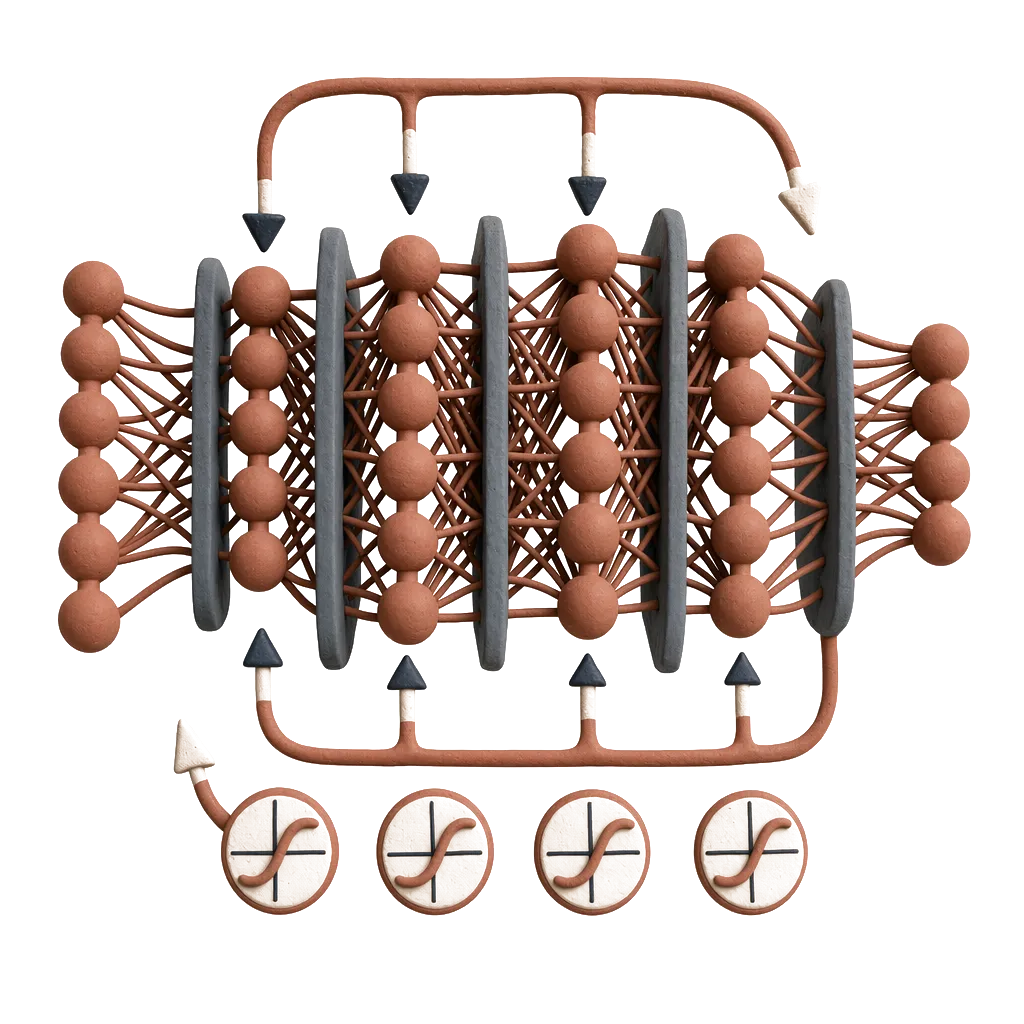
Offline learning performance with quantization-aware training can be demonstrated with the MNIST dataset of handwritten digits [27]. Using the four cores of MorphIC and all the available neuron resources with the network topology shown in Fig. 12, an accuracy of 97.8% is reached using conventional rate-based coding (i.e. the spike frequency of a neuron encodes its output value). As the synaptic weights trained in Keras have 1 and 1 values while the MorphIC synapses have 0 and 1 values instead, it is necessary to compensate for the asymmetric weight distribution of MorphIC. This compensation can be made in a layer by subtracting half the sum of its inputs, which can be achieved by layer-wise inhibitory neurons connected with weight 1 to all the layer inputs and having a firing threshold of 2, as shown in Fig. 12. As the rate code is inefficient in its spike use, it results in a high energy per classification of 205J at 0.8V and 55MHz. It has been shown in [20] that the rank order code (i.e. values are encoded in the order in which neurons spike) is a simple yet much more efficient coding strategy than rate coding. The inferred class can be retrieved from the neuron in the output layer that spikes first. Using rank order coding, MorphIC consumes 5.45mW for 250 classifications per second at 0.8V and 55MHz, which allows reaching a 10-fold energy improvement down to 21.8J per classification, at the expense of a drop of 1.9% in accuracy. The energy-accuracy tradeoff of MorphIC will be discussed and compared to the state of the art in Section IV-C.
S-SDSP online learning is demonstrated in Fig. 13, we reproduced the benchmark that was proposed in [34] for an analog SDSP implementation. Eight patterns are classified by a spiking CNN. Each MorphIC core implements a fixed-weight convolutional layer with a line detection kernel followed by an average pooling layer. The pooling layers from cores 1 to 3 are then mapped back to core 0 through L1 connectivity so as to form a single flattened layer. The flattened layer is connected with plastic weights to an 8-neuron fully-connected (FC) output layer in core 0. The resulting weights allow correctly discriminating all test samples in a test set consisting of 100 different Poisson realizations of each input pattern.
IV Discussion
Comparison with the state of the art can be carried out along several axes, all of which lead to guidelines for future work. Section IV-A compares the proposed hierarchical event routing infrastructures with previously-proposed approaches. Section IV-B discusses the implementation strategy of the proposed S-SDSP learning rule. Section IV-C analyzes the area-accuracy and energy-accuracy tradeoffs on the MNIST dataset. Finally, Section IV-D compares MorphIC with the three binary-weight SNNs proposed to date: TrueNorth [15], Loihi [16] and the chip from Seo et al. [17].
IV-A Hierarchical event routing
A key feature of MorphIC is that only 27 bits per neuron are required to entirely define the connectivity of a multi-chip network, while the routers at all the hierarchy levels are memory-less beyond simple event buffering (i.e. no dedicated access to a stored mapping table). This contrasts with Neurogrid [25] and HiAER [23], which achieve low-cost large-scale routing at the expense of requiring external mapping table storage, thus indirectly inducing high resource and power overheads. SpiNNaker [35, 24] embeds the largest-scale multicast connectivity infrastructure proposed so far. It avoids external accesses but requires local mapping tables inside the routers to store all connectivity information for source-based 2-D triangular toroidal mesh-based routing. The same holds for DYNAPs [22], which also avoids external accesses but still requires local 2.5-kB SRAM storage in the R1 router of each 256-neuron core, beyond a CAM-based 640-bit tag storage per neuron that allows reaching a high fan-out of 4k at the expense of density. Moreover, in DYNAPs, the synaptic connections are defined within the connectivity infrastructure, as opposed to MorphIC which has independent online-learning synapses on the top of the connectivity infrastructure. Therefore, none of Neurogrid, HiAER, SpiNNaker or DYNAPs offer low-cost memory-less routers throughout the hierarchy. The routing infrastructure of TrueNorth [15] holds similar advantages to the one of MorphIC: the routers are also memory-less and require neither external nor internal storage. However, there are only two levels in the TrueNorth hierarchy: the 64k-synapse 256-neuron crossbar cores and the large-scale mesh-based routers. While an arbitrary number of neurons can map to the same axons111Axons are defined as inputs in the TrueNorth terminology, each axon connecting to 256 neurons through 256 synapses in a local crossbar array., thus reaching arbitrary fan-ins with 256 shared synapses, the neuron fan-out of TrueNorth is limited to a maximum value of 256+256. In MorphIC, the addition of an intermediate L1 star-based router brings a two-fold advantage over TrueNorth: it divides by two the number of L2 hops between any two cores and allows extending the neuron fan-out. Finally, the hierarchical routing infrastructure of Loihi [16] differs strongly from all other previously-proposed approaches and, as DYNAPs, does not rely on a crossbar operation at the lowest level of the hierarchy. Instead, it is highly configurable in order to adapt to the target application: 120-kB SRAM memories are used to store the entire synaptic fan-in state of each core, which allows trading off the number of synapses with flexibility in the connectivity patterns. The high-level routing infrastructure of Loihi relies on a unicast mesh-based NoC: in order to process neuron spike multicasting with up to 4096 output axons, one packet needs to be generated for each destination. Therefore, Loihi achieves multicasting at the expense of high router load overhead. While the three-level connectivity infrastructure of MorphIC is less flexible, multicasting is only handled at the L1 level and a clear hierarchy segmentation avoids overloading higher-level routers. It ensures that the higher the hierarchy, the sparser the events and the higher the level of the encoded features, which leads to high efficiency if the hierarchical nature of the event routing infrastructure matches the intrinsic hierarchy in the data representation of a given task. In the case of MorphIC, as shown in Section III, the chosen hierarchical routing infrastructure is ideal to process tasks of the complexity of MNIST in a single chip. The cores implement four weak classifiers that carry out inference on independent sub-images, star-based L1 routing allows all cores to be at equidistance (as opposed to mesh-based routing) to combine weak classifications in a single core, while L2 routing is used to transmit sparse spikes encoding the inference on the full MNIST image.
As the hierarchical event routing fabric of MorphIC strongly relies on all-to-all crossbar operation (Fig. 6), the proposed connectivity infrastructure is ideal to explore fully-connected and recurrent network configurations. Though convolutional layers can also be implemented using crossbars, the absence of efficient weight reuse implies copying the kernels in the dendritic tree of each output neuron. As the receptive field of each neuron in a convolutional layer usually consists of only a few inputs, there is a poor utilization of the synaptic fan-in resources while the time-multiplexed controller goes through a majority of dummy SOPs with zero weights (Fig. 4). The latter aspect can be mitigated by a controller update, similarly to the crossbar optimization with start and end addresses proposed in Section IV-C for fully-connected layers.
Finally, it is worth noting that all the routers in the aforementioned approaches operate asynchronously, except in HiAER [23] and MorphIC. In MorphIC, the choice of clocked operation for the routers allows for a straightforward design at the expense of efficiency. Indeed, the timing critical path being located at the core level, using one global clock common to both the cores and the routers unnecessarily limits the bandwidth of the latter which, as they are memory-less, could operate at much higher speed. Asynchronous router design would alleviate this problem. In order to avoid the design time and complexity overhead of asynchronous digital design, another option would be to locally generate a high-speed clock directly in the L1 and L2 routers, for example with a local ring oscillator that is enabled only when packets await routing.
IV-B S-SDSP online learning
The development of silicon implementations for bio-inspired learning rules such as STDP and SDSP is an inherently bottom-up process: the first step lies in neuroscience experimentation to understand biological phenomena, the second step lies in the development of efficient analog or digital circuits that emulate neuroscience observations, the third step consists in finding a suitable application. Therefore, while bottom-up approaches lead to efficient silicon implementations of bio-inspired plasticity models and are ideal for the design of experimentation platforms, bridging the gap from local brain-inspired learning toward more complex real-life applications is difficult. To the best of our knowledge, only simplified benchmarks have been used so far to demonstrate silicon implementations of STDP, SDSP or their variations. A summary is provided in Table III: no STDP- or SDSP-based learning rule has yet been successfully applied in silico to at least the full MNIST dataset without any pre-processing step. The S-SDSP learning rule we propose for MorphIC allows reaching the highest density of online-learning synapses and has successfully been demonstrated on the 8-pattern benchmark from [34]. However, as it also follows from a bottom-up design approach, scaling S-SDSP to more complex tasks is not straightforward as it would require going beyond single-layer training. Further research is required to leverage brain-inspired local plasticity primitives with multi-layer networks for online learning on real-world tasks, as highlighted by the recent S-STDP study by Yousefzadeh et al. [37].
On the other hand, top-down approaches start from the applicative problems (e.g., image recognition), where the successful backpropagation of errors algorithm [38] has already been applied to specific datasets such as MNIST, CIFAR-10 or ImageNet. Such approaches then attempt to design variations of the backpropagation algorithm that are more in line with brain observation, such as moving data representation to spiking or dropping the requirement for symmetric weights [11, 39]. Silicon implementations would come as a last step. In order to overcome the challenges of bottom-up approaches, the development of new multi-layer spike-based learning rules following top-down approaches has gained growing interest in the recent years (e.g., [9, 10, 11, 12]). Further research is yet required to realize efficient silicon implementations of such learning rules and to make them both compatible with an online-learning setup and able to leverage weight quantization down to binary or ternary resolutions.
Finally, regarding the synapse implementation, we showed in Section II-B that our S-SDSP design is compatible with a standard single-port foundry SRAM, which holds a strong advantage in design time and density over custom-SRAM-based designs, such as in [17]. Our foundry-SRAM-based S-SDSP approach therefore allows leveraging high-density integration of binary plastic synapses. There are two other main trends for synapse implementation. First, the capacitor-based approach proposed in [40] for the subthreshold analog 0.18-m ROLLS chip allows emulating SDSP dynamics with biological time constants and a resolution of a few bits, at the expense of synaptic mismatch and a critical silicon footprint for the pF-range capacitor inside each synapse. Therefore, technology scaling pushes recent subthreshold analog developments to move synaptic weights to TCAM and SRAM memories [41]. Second, non-volatile memories for crossbar implementations leveraging in-memory computation with novel technologies are currently being actively explored. On the one hand, a flash-based approach with STDP plasticity was successfully prototyped in 0.35m CMOS in [42], however embedded flash memory is difficult to scale beyond 40nm and requires high programming voltages. On the other hand, memristors promise new density records and recent work (e.g., [43]) shows how the memristor characteristics can be used to emulate biological synapses and to implement stochastic learning, but high-yield co-integration with CMOS has yet to be demonstrated. For both flash- and memristor-based approaches, the aspects linked to synaptic resolution control, mismatch and fabrication costs will have to be alleviated. It therefore appears that the foundry-SRAM-based strategy that we propose is currently a sound strategy for an efficient low-cost synapse array design.
IV-C Tradeoff analysis of energy, area and accuracy
An analysis of the energy, area and accuracy tradeoffs is shown in Fig. 14, where MorphIC is compared to other SNNs that have been demonstrated on the full 2828 MNIST dataset with no pre-processing beyond conversion of pixel values to spikes: the SNNs from Chen et al. [14], from Kim et al. [44], from Buhler et al. [45] and TrueNorth, which was benchmarked on MNIST in [46]. In order to carry out comparison in a one-to-one basis, all area and energy numbers have been normalized to a 65-nm technology node. While we keep this comparison focused on SNNs, there is also a large body of work for efficient MNIST-proven frame-based neural network accelerators: we refer the reader to [1] for a partial review and to [47] for a recent example.
The area-accuracy tradeoff is shown in Fig. 14(a): MorphIC achieves an order-of-magnitude improvement compared to previously-proposed SNNs. The energy-accuracy tradeoff is shown in Fig. 14(b). While rate coding allows reaching the highest accuracy for MorphIC, the associated power inefficiency is clearly illustrated. Rank order coding (Section III) allows reaching an energy-accuracy tradeoff that comes close to TrueNorth and the SNN from Chen et al. [14]. Following the MorphIC power model from Eq. (3), we can break down the rank-order energy per inference of 21.8J at 0.8V and 55MHz as follows: . Three simple improvements to the MorphIC architecture or implementation would allow to reduce these contributions, as shown in Fig. 14(b) and detailed in Table IV. First, while crossbar operation is highly-efficient for the implementation of fully-connected layers, systematic processing of all neurons in the array for each input spike can lead to a lot of dummy operations (e.g., as shown in Fig. 12, a neuron from the hidden layer should lead to only 10+1 SOPs toward the output layer neurons, not 512). This could be improved by adding only two 9-bit parameters per neuron that define the start and end indices of the destination neurons. Adding this architectural improvement to MorphIC would reduce the number of SOPs to be processed and thus the time per inference, bringing down to 16.0J per inference. Second, as shown in Fig. 12, inhibitory neurons have been added to the hidden and output layers to compensate for rescaling of the synaptic weights trained offline with and values to [math] and values in MorphIC. However this comes at the expense of a 50-% increase in SOP activity. In combination with the previous improvement, allowing the MorphIC binary weights to be interpreted as and values instead of [math] and would allow to further reduce to 10.7J per inference. Finally, as clock gating has only been inserted automatically by the synthesis tool, simple architectural clock gating could be applied (i) to the parameter banks after initial chip configuration and (ii) to S-SDSP up/down registers (Fig. 3) during inference. This would lead to an idle power reduction by 55%, further optimizing down to a value of 8.2J per inference.
Therefore, MorphIC demonstrates an order-of-magnitude improvement in the area-accuracy tradeoff on the MNIST classification task, while keeping an energy-accuracy tradeoff comparable to TrueNorth and the SNN from Chen et al. [14]. With a low leakage of only 45W at 0.8V to ensure full retention of the neuronal and synaptic data, MorphIC is ideally-suited for always-on event-driven processing.
IV-D Comparison with previously-proposed binary SNNs
A comparison of MorphIC with the three previously-proposed binary SNNs is provided in Table V. As TrueNorth embeds static weights and Loihi has a programmable learning engine but does not demonstrate online learning with a binary-weight configuration, MorphIC and the chip from Seo et al. [17] are the only ones to demonstrate embedded online learning on binary weights. The high-density claim of binary-weight S-SDSP online learning is demonstrated with an order-of-magnitude advantage compared to the S-STDP rule from Seo et al. [17]. This point is further emphasized when considering process normalization to 65nm, illustrating record densities for MorphIC. Regarding power, MorphIC has an energy per SOP similar to the other binary SNNs despite using a less advanced CMOS process.
V Conclusion
In this paper, we presented the MorphIC quad-core spiking neuromorphic processor to leverage binary weights with online-learning SNNs. Using the proposed stochastic spike-dependent synaptic plasticity (S-SDSP) learning rule, we demonstrated this claim with a density of 738k synapses per mm2 in 65nm CMOS. MorphIC shows order-of-magnitude improvements both in the area-accuracy tradeoff on MNIST compared to other SNNs and in density compared to the only previously-proposed binary SNN with demonstrated online learning from Seo et al. [17]. MorphIC also integrates a low-cost hierarchical routing fabric with low-memory connectivity for large-scale chip interconnection, where distance information allows modulating the synaptic update probabilities, in accordance with small-world brain network modeling.
Acknowledgment
The authors would like to thank Europractice and its First User Stimulation Program for chip prototyping. C. Frenkel is with Université catholique de Louvain as a Research Fellow from the National Foundation for Scientific Research (FNRS) of Belgium.
The reference list from the paper itself. Each links out to its DOI / PubMed record.
- 1[1] P. N. Whatmough et al., “A 28nm So C with a 1.2 G Hz 568n J/prediction sparse deep-neural-network engine with > > 0.1 timing error rate tolerance for Io T applications,” Proc. of IEEE International Solid-State Circuits Conference (ISSCC) , 2017.
- 2[2] B. Moons et al., “Minimum energy quantized neural networks,” Proc. of IEEE Asilomar Conference on Signals, Systems, and Computers , 2017.
- 3[3] M. Courbariaux et al., “Binarized neural networks: Training deep neural networks with weights and activations constrained to +1 or -1,” ar Xiv preprint ar Xiv:1602.02830 , 2016.
- 4[4] R. Andri et al. “Yoda NN: An architecture for ultralow power binary-weight CNN acceleration,” IEEE Transactions on Computer-Aided Design of Integrated Circuits and Systems , vol. 37, no. 1, pp. 48-60, 2018.
- 5[5] B. Moons et al., “Binar Eye: An always-on energy-accuracy-scalable binary CNN processor with all memory on chip in 28nm CMOS,” Proc. of IEEE Custom Integrated Circuits Conference (CICC) , 2018.
- 6[6] D. Bankman et al., “An always-on 3.8 μ 𝜇 \mu J/86% CIFAR-10 mixed-signal binary CNN processor with all memory on chip in 28nm CMOS,” Proc. of IEEE International Solid-State Circuits Conference (ISSCC) , 2018.
- 7[7] C. S. Poon and K. Zhou, “Neuromorphic silicon neurons and large-scale neural networks: challenges and opportunities,” Frontiers in neuroscience , vol. 5, p. 108, 2011.
- 8[8] M. R. Azghadi et al., “Spike-based synaptic plasticity in silicon: design, implementation, application, and challenges,” Proceedings of the IEEE , vol. 102, no. 5, pp. 717-737, 2014.