Direct observation of minibands in twisted heterobilayers
S{\o}ren Ulstrup, Roland J. Koch, Simranjeet Singh, Kathleen M., McCreary, Berend T. Jonker, Jeremy T. Robinson, Chris Jozwiak, Eli Rotenberg,, Aaron Bostwick, Jyoti Katoch, Jill A. Miwa

TL;DR
This study directly observes minibands in twisted graphene-WS2 heterobilayers using advanced microARPES, demonstrating control over quantum states through stacking angle, which could lead to novel 2D material functionalities.
Contribution
Introduces a new X-ray capillary microARPES technique to map minibands in 2D heterobilayers, revealing angle-dependent miniband formation in graphene-WS2 systems.
Findings
Minibands observed at 2.5° twist angle
No minibands at 26.3° twist angle
Control of quantum states via stacking configuration
Abstract
Stacking two-dimensional (2D) van der Waals materials with different interlayer atomic registry in a heterobilayer causes the formation of a long-range periodic superlattice that may bestow the heterostructure with exotic properties such as new quantum fractal states [1-3] or superconductivity [4, 5]. Recent optical measurements of transition metal dichalcogenide (TMD) heterobilayers have revealed the presence of hybridized interlayer electron-hole pair excitations at energies defined by the superlattice potential [6-10]. The corresponding quasiparticle band structure, so-called minibands, have remained elusive and no such features have been reported for heterobilayers comprised of a TMD and another type of 2D material. Here, we introduce a new X-ray capillary technology for performing micro-focused angle-resolved photoemission spectroscopy (microARPES) with a spatial resolution on the…
Click any figure to enlarge with its caption.
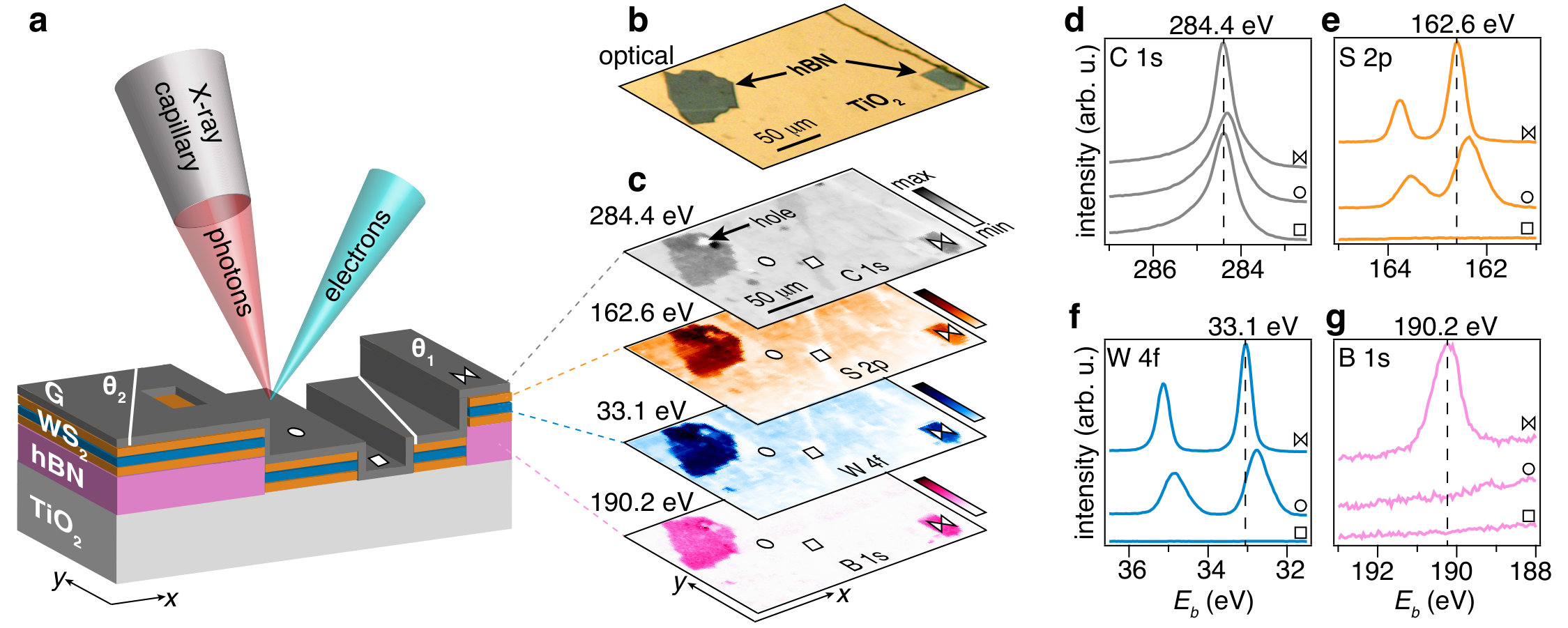 Figure 1
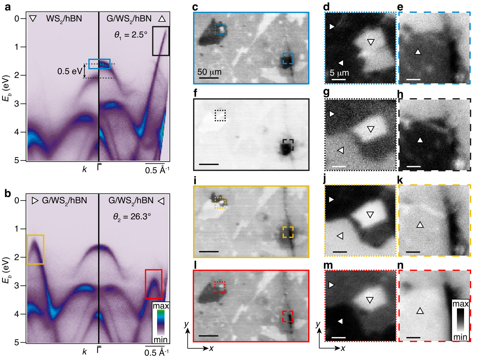 Figure 2
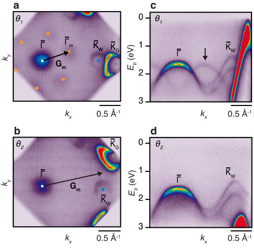 Figure 3
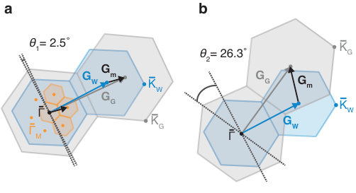 Figure 4
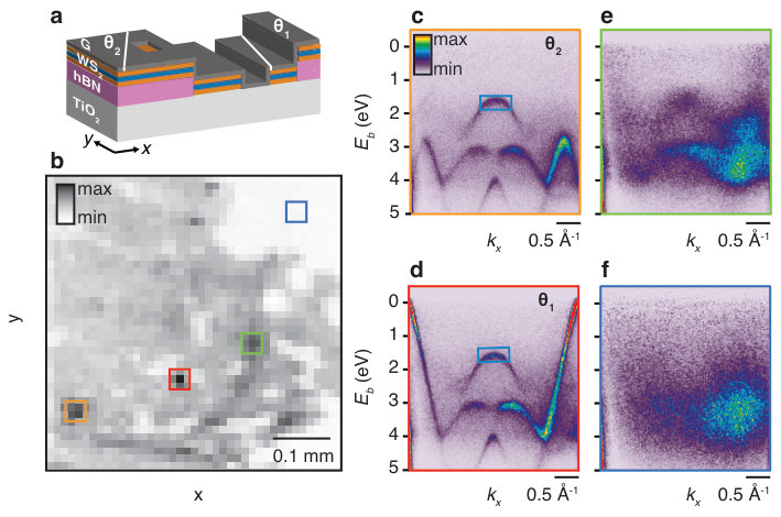 Figure 5
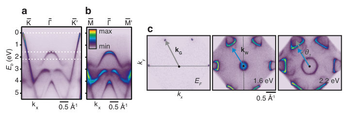 Figure 6
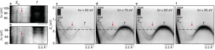 Figure 7
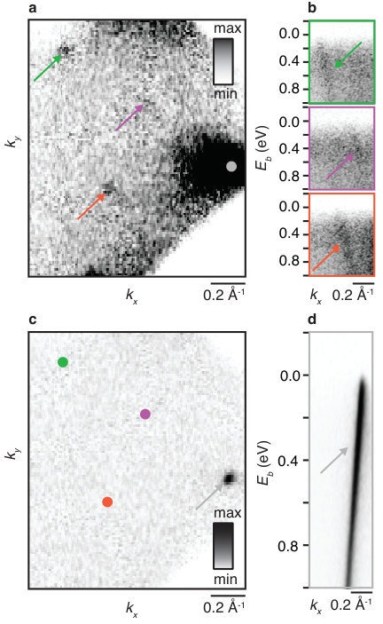 Figure 8
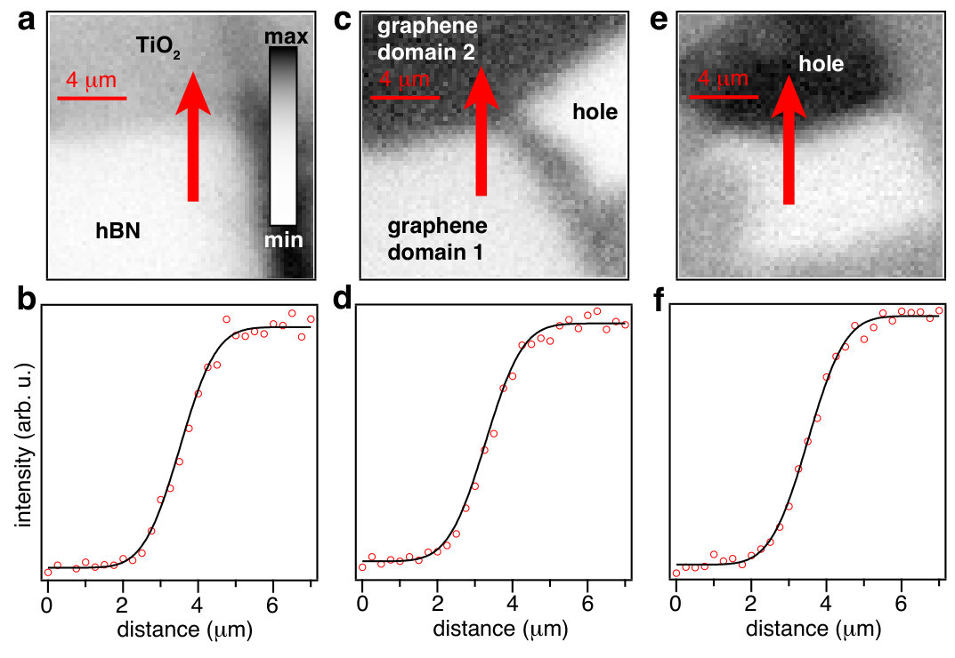 Figure 9
Peer Reviews
No public reviews on file for this paper yet. If you reviewed it on a platform where reviews are public (OpenReview, ICLR, NeurIPS, ICML), you can paste yours below so the community can read it here.
Videos
No videos yet. Explain this paper in a talk, walkthrough, or lecture? Add one.
Direct observation of minibands in twisted heterobilayers
Søren Ulstrup
Department of Physics and Astronomy, Aarhus University, 8000 Aarhus C, Denmark
Roland J. Koch
Advanced Light Source, E. O. Lawrence Berkeley National Laboratory, Berkeley, California 94720, USA
Simranjeet Singh
Department of Physics, Carnegie Mellon University, Pittsburgh, Pennsylvania 15213, USA
Kathleen M. McCreary
Naval Research laboratory, Washington, D.C. 20375, USA
Berend T. Jonker
Naval Research laboratory, Washington, D.C. 20375, USA
Jeremy T. Robinson
Naval Research laboratory, Washington, D.C. 20375, USA
Chris Jozwiak
Advanced Light Source, E. O. Lawrence Berkeley National Laboratory, Berkeley, California 94720, USA
Eli Rotenberg
Advanced Light Source, E. O. Lawrence Berkeley National Laboratory, Berkeley, California 94720, USA
Aaron Bostwick
Advanced Light Source, E. O. Lawrence Berkeley National Laboratory, Berkeley, California 94720, USA
Jyoti Katoch
Department of Physics, Carnegie Mellon University, Pittsburgh, Pennsylvania 15213, USA
Jill A. Miwa
Department of Physics and Astronomy, Aarhus University, 8000 Aarhus C, Denmark
Stacking two-dimensional (2D) van der Waals materials with different interlayer atomic registry in a heterobilayer causes the formation of a long-range periodic superlattice that may bestow the heterostructure with exotic properties such as new quantum fractal states Dean et al. (2013); Ponomarenko et al. (2013); Hunt et al. (2013) or superconductivity Cao et al. (2018); Yankowitz et al. (2019). Recent optical measurements of transition metal dichalcogenide (TMD) heterobilayers have revealed the presence of hybridized interlayer electron-hole pair excitations at energies defined by the superlattice potential Kunstmann et al. (2018); Alexeev et al. (2019); Jin et al. (2019); Seyler et al. (2019); Tran et al. (2019). The corresponding quasiparticle band structure, so-called minibands, have remained elusive and no such features have been reported for heterobilayers comprised of a TMD and another type of 2D material. Here, we introduce a new X-ray capillary technology for performing micro-focused angle-resolved photoemission spectroscopy (microARPES) with a spatial resolution on the order of 1 m, enabling us to map the momentum-dependent quasiparticle dispersion of heterobilayers consisting of graphene on WS2 at variable interlayer twist angles (). Minibands are directly observed for in multiple mini Brillouin zones (mBZs), while they are absent for a larger twist angle of . These findings underline the possibility to control quantum states via the stacking configuration in 2D heterostructures, opening multiple new avenues for generating materials with enhanced functionality such as tunable electronic correlations Wu et al. (2018) and tailored selection rules for optical transitions Ruiz-Tijerina and Fal’ko (2019).
Assembling single-layer (SL) TMDs with different electronic structures in heterobilayers has emerged as a promising method for tailoring the band alignment at type-II heterojunctions Chiu et al. (2015); Wilson et al. (2017), offering a means to control optical excitation and charge transfer processes at the atomic scale Hong et al. (2014). This approach to materials design inevitably involves joining two crystal lattices with different lattice constants and orientation. The long-range periodic pattern arising from the superposition of interlayer atomic registries produces a moiré superlattice. Scanning tunneling microscopy/spectroscopy (STM/STS) experiments on heterobilayers of TMDs have resolved such a moiré together with a local band gap modulation due to the superlattice potential Zhang et al. (2017). In ARPES, these superlattice effects are directly observable via the formation of minibands such as the mini Dirac cones identified in epitaxial graphene on Ir(111) Pletikosić et al. (2009); Starodub et al. (2011), twisted bilayer graphene Ohta et al. (2012) and heterostructures of graphene with hexagonal boron nitride (hBN) Wang et al. (2016a, b). Since ARPES directly probes the energy- and momentum-resolved quasiparticle excitation spectrum, these measurements provide critical information about the minibands such as dispersion, hybridization with main bands, opening of mini gaps as well as emergence of correlation effects i.e., properties that completely specify the functionality of the heterostructure.
It has so far not been possible to observe similar minibands in epitaxial SL TMDs on single-crystal metal substrates Miwa et al. (2015) or TMDs on bilayer graphene on silicon carbide Zhang et al. (2013); Ugeda et al. (2014) despite visible moiré superlattices in the STM data Miwa et al. (2015); Ugeda et al. (2014); Kastl et al. (2018). Recent optical studies of TMD heterobilayers, however, show distinct exciton lines arising from twist angle dependent minibands Alexeev et al. (2019); Jin et al. (2019); Seyler et al. (2019); Tran et al. (2019). It is plausible that the signature of the quasiparticle minibands may have been suppressed in these earlier ARPES measurements due to stronger TMD-substrate interactions, long-range rotational disorder, and/or quenching of the interlayer photoemission intensity as a result of the three-atomic-layer (sandwich-like) structure which essentially constitutes a SL TMD, effectively “burying” the interface. Furthermore, the epitaxial approach in these studies did not allow for tuning of layer orientation, thereby preventing a systematic search for minibands in materials with a different moiré superlattice.
We resolve these issues by using a new microARPES approach with a spatial resolution on the order of 1 m to measure a heterobilayer consisting of graphene, SL WS2 and hBN. Both the graphene and the SL WS2 were grown by chemical vapor deposition (CVD) and sequentially transferred onto the hBN. The graphene has multiple domain orientations while the SL WS2 is single domain. The resulting graphene/WS2/hBN stack is supported on a TiO2 wafer; see illustration in Fig. 1(a) and optical microscope image of hBN flakes on TiO2 in Fig. 1(b). The atomically flat interface and vanishing interlayer interactions with hBN facilitate the collection of extremely high-quality ARPES spectra as recently demonstrated for bare WS2/hBN Katoch et al. (2018). The CVD grown graphene provides a multitude of different orientations on top of WS2, giving access to domains with different twist angles (-domains). The interface of the heterobilayer is notably situated below a single carbon layer instead of the sandwich-like structure of the SL TMD, thereby greatly enhancing the photoemission intensity from the interface compared to earlier studies. Each interface type and -domain is measured by scanning the micro-focused beam of photons across the same area of the sample as seen in the optical microscope image in Fig. 1(b), leading to photoemission from microscopic points on the sample. The focusing is achieved using an achromatic X-ray capillary, providing efficient mapping of valence band (VB) and core level binding energy regions due to a high photon flux and highly tunable photon energy range compared to conventional X-ray focusing optics such as Fresnel zone plates Sakdinawat and Attwood (2010); Koch et al. (2018); Kastl et al. (2019).
Photoemission intensity maps acquired at core level peak energies characteristic of the 2D materials in the heterostructure are shown in Fig. 1(c). Each -position in a map contains a measurement of the corresponding core level binding energy region as shown for the points marked by the symbols “”, “” and “” for C 1s in panel (d), S 2p in panel (e), W 4f in panel (f) and B 1s in panel (g). The contrasts provided by the peak amplitude, position and linewidth clearly outline the graphene/TiO2 (), graphene/WS2/TiO2 () and graphene/WS2/hBN/TiO2 () interfaces. We also identify a hole in the transferred graphene, exposing a bare WS2/hBN area as seen via an arrow in the C 1s map in panel (c). The spectral linewidths of W 4f, S 2p and C 1s core levels obtained on hBN (marked by the ) are reduced by a factor of 2 compared to those measured on the TiO2 (marked by the ). Similar conclusions can be made for the linewidths of the VB spectra as discussed in further detail in the Supplementary Section 1, which we attribute to the flatness and extremely weak charge impurity scattering in hBN compared to the oxide.
We determine the energy- and momentum-dependent dispersion relation, , in the VB region, as shown in Figs. 2(a)-(b). The spectra are characterized by a mix of graphene bands (see black, yellow and red boxes) and the WS2 VB manifold (see blue box for the local VB maximum (VBM) at ). Interestingly, we find that the graphene pins the WS2 electronic structure by a rigid shift of 0.5 eV compared with the WS2 states measured on a bare WS2/hBN region of the sample; see double-headed arrow in Fig. 2(a). The presented data are only a subset of spectra from a 4-dimensional data set containing the -dependent photoemission intensity. It is furthermore possible to obtain corresponding cuts of the intensity in real space composed from a specified region of -space. The results of projecting the specified electronic band structure on a -dependent intensity map are shown in Figs. 2(c)-(n). Panels (c)-(e) are -maps derived from the WS2 local VBM at . The map in panel (c) is a coarse scan corresponding to the field of view in Figs. 1(b)-(c) while the maps in panels (d)-(e) are fine scans of the regions demarcated by dotted and dashed boxes in panel (c). High (low) intensity in real space allows us to identify the presence (absence) of WS2 electronic states at energies and momenta determined by the blue box in panels (a)-(b). Similarly, the -maps in panels (f)-(n) track the domains with the graphene bands given by the -cuts in the black, yellow and red boxes in panels (a)-(b). Measurements of the full 2D Brillouin zone (BZ) permit the determination of , as explained in the Supplementary Section 2. Here we focus on the two -domains seen via high intensity in panels (f) and (l) (see also symbols “” and “” in Fig. 2) where we find two significantly different twist angles given by and . We also observe another orientation in panel (i) (marked by a “” in Fig. 2) but this graphene/WS2 interface has a m hole (marked by a “” in Fig. 2), which led to spurious features in the BZ maps we collected from this domain preventing a detailed analysis of the twist angle.
Figs. 3(a)-(b) map in two momentum directions, and , the constant-energy contours at a binding energy of approximately 1.6 eV for the - and -domains. In both maps, the three most prominent features are labelled , W and G; these labels correspond to the nearly circular feature of the WS2 band at , the spin-split bands of WS2 at W, and the horseshoe-shaped arcs of the graphene Dirac cones at G. There are faint circular features surrounding in panel (a) that are notably absent in panel (b). These features are ascribed to minibands, labelled as m, and are replicas of the WS2 band at that arise from the periodic potential of the -domain, established by the twist angle of 2.5 ∘ between the graphene and WS2 lattices. From the dispersion of the bands, acquired along the –W direction as shown in Fig. 3(c), we see that the miniband, highlighted by the black arrow, replicates the overall shape of the SL WS2 band at . No miniband is present in the similarly acquired -plot of Fig. 3(d) for the -domain, where the twist between the graphene and SL WS2 lattices is at a substantially larger angle of 26.3 ∘. As described in Supplementary Section 3, the intensity of the WS2 minibands peaks in the photon energy range of 60-70 eV and appears to exhibit a strong -dependence in agreement with recent theoretical predictions of the one-electron dipole matrix elements calculated for the photoemission process involving van der Waals heterostructures Amorim (2018).
The positions of the minibands in -space are determined by addition of the reciprocal lattice vectors of graphene () and WS2 (), as illustrated in Fig. 4. Two adjacent 2D BZs of graphene (grey hexagons) are superimposed on two adjacent 2D BZs of WS2 (blue hexagons) with twist angles matching those of - and -domains. From the reciprocal lattice vectors, we establish the moiré reciprocal lattice vector () and construct the corresponding mBZs (orange hexagons) by replicating around the point to locate the centers (orange dots) of the surrounding mBzs. The position of the minibands are mathematically confirmed using the following expressions for the angles and magnitude of the moiré vector: and . Indeed, we find that for the -domain (-domain): Å*-1* (1.35 Å*-1*), (49.1*∘) for the angle between and , and (75.4∘*) for the angle between and . All magnitudes of the reciprocal lattice vectors and angles are in agreement with the microARPES data obtained for these two domains shown in Fig. 3 within the experimental accuracy. The minibands are absent in the case of the -domain as the superlattice potential gets weaker at high twist angles leading to a reduced photoemission intensity. This result is both consistent with theoretical calculations Amorim (2018) and photoemission results of epitaxial graphene on Ir(111) Starodub et al. (2011), and with detailed theory on the origins of minibands in TMD/TMD heterobilayers Ruiz-Tijerina and Fal’ko (2019). The observation of WS2 minibands also implies the existence of mini Dirac cones replicated by the same reciprocal lattice vector in the graphene. Indeed, we find mini Dirac cones at the expected -space coordinates, but their intensity is extremely faint, as shown in the Supplementary Section 4. This observation also confirms that the minibands derive from the graphene/WS2 and not the WS2/hBN interface. Moreover, we do not observe any superlattice features from the bare WS2/hBN interface in the hole (see the “” in Fig. 2) nor in any earlier studies Katoch et al. (2018), possibly due to this interface being buried below the TMD sandwich-like structure. For the sake of clarity, we have omitted the hBN 2D BZ in the sketches in Fig. 4 as this interface does not contribute to our observations.
In summary, we have directly measured the quasiparticle band structure for a graphene/WS2 heterobilayer on hBN using a new X-ray capillary technology for carrying out microARPES. In particular, we capitalize on the 1 m spatially resolving capabilities afforded by this technique to not only determine different interlayer twist angles between the graphene and WS2 but to directly measure minibands produced by the resulting superlattice potential. The technique itself allows for a systematic search of quasiparticle band structures that emerge from moiré superlattices in van der Waals heterostructures. We believe that this is a key observation that not only compliments recent optical studies that have revealed moiré excitons in TMD/TMD heterobilayers Alexeev et al. (2019); Jin et al. (2019); Seyler et al. (2019); Tran et al. (2019) but also demonstrates that our microARPES approach is an ideal strategy towards superlattice engineering of band structure and correlations in 2D materials. The presence of minibands for both SL WS2 and graphene implies the possibility to simultaneously excite moiré excitons in SL WS2 and generate quantum fractal states in the neighboring graphene, all within the same material stack. We therefore expect that our results will inspire further experimental and theoretical studies of the interplay of these effects in multifunctional heterobilayer materials.
I Methods
Graphene growth on Copper. Graphene films were grown using low-pressure CVD with flowing H2 and CH4 gases Zhu et al. (2011). Before growth, the copper foils were electrochemically polished to improve surface cleanliness and remove oxides. These copper foils were then folded into ‘packets’ Li et al. (2011), loaded into a quartz tube and pumped to a base pressure of 2 mTorr. The copper substrates were heated to 1030 *∘*C and H2/CH4 was introduced for 1.5 hours at a total pressure of 60 mTorr. The substrates were then quenched by removing them from the hot zone while under vacuum.
Single-layer WS2 growth on SiO2/Si. Synthesis of SL WS2 was performed at ambient pressure in a 2-inch diameter quartz tube furnace on SiO2/Si substrates (275 nm thickness of SiO2). Prior to use, all SiO2/Si substrates were cleaned in acetone, isopropanol, and Piranha etch then thoroughly rinsed in DI water. At the center of the furnace a quartz boat containing 1 g of WO3 powder was positioned. Two SiO2/Si wafers were positioned face-down, directly above the oxide precursor. The upstream wafer contained perylene-3,4,9,10-tetracarboxylic acid tetrapotassium salt (PTAS) seeding molecules, while the downstream substrate was untreated. The hexagonal PTAS molecules were carried downstream to the untreated substrate and promoted lateral growth of the TMD materials. A separate quartz boat containing sulfur powder was placed upstream, outside the furnace-heating zone. Pure argon (65 sccm) was used as the furnace was heated to the target temperature. Upon reaching the target temperature of 825 *∘*C, 10 sccm H2 was added to the Ar flow and maintained throughout the 10 minute soak and subsequent cooling.
Heterostructure fabrication. Bulk hBN crystals were exfoliated onto a -doped TiO2 substrate using scotch tape to obtain 10–30 nm thick flakes. The TiO2 substrate with exfoliated hBN flakes was annealed in ultra-high vacuum (UHV) at 150 *∘*C for 15 minutes to get rid of any unwanted tape residues. Next, CVD grown single-domain SL WS2 was transferred onto the cleaned hBN flakes using a thin PC film on a PDMS stamp employing a custom-built transfer tool Katoch et al. (2018); Ulstrup et al. (2016). This was followed by another annealing cycle of the WS2/hBN heterostructure in UHV at 150 *∘*C for 15 minutes. Separately, one side of the copper foil (with graphene grown on both sides) was spin coated with a PMMA layer. The CVD graphene layer on the backside (without protective PMMA layer) of the copper foil was etched away using reactive ion etching. Next, the PMMA/graphene was floated by etching away the copper using wet chemistry Patra et al. (2012); Singh et al. (2015). The PMMA/graphene layer was subsequently transferred onto a clean WS2/hBN stack. The top PMMA layer was removed by immersing the graphene/WS2/hBN heterostructure in acetone for 15 minutes followed by a rinse in isopropanol. Lastly, the graphene/WS2/hBN heterostructure was subjected to another annealing cycle in UHV.
Spatially-resolved ARPES experiments. The heterobilayer sample was shipped in air and inserted into the Microscopic and Electronic Structure Observatory (MAESTRO) UHV facility at the Advanced Light Source (ALS) in Berkeley. The sample was annealed at 600 K for 15 minutes prior to ARPES measurements.
The micro-focused scanning of core level and ARPES spectra presented in Figs. 1-2 was carried out in the MAESTRO nanoARPES end-station using an X-ray capillary (Sigray Inc.) with a spatial resolution in this experiment given by m, as explained in the Supplementary Section 5. We used a coarse-motion piezo scanner for spatial maps larger than 30 m with a step-size of 1.5 m and a fine-motion piezo flexure scanning stage for detailed maps below this range and with a scanning step of 250 nm. Due to the achromaticity of the capillary we were able to perform valence band measurements with variable photon energy in the range 60-160 eV and W 4f, S 2p, B 1s and C 1s core level measurements with a photon energy of 350 eV without apparent loss of spatial resolution. The high efficiency of the capillary enabled acquisition of 4D datasets of the -dependent intensity in 40 minutes. The -dependent data presented in Fig. 3 were collected using an electron analyzer equipped with custom-made deflectors in the MAESTRO microARPES end-station, such that the sample could be held fixed during BZ mapping. These measurements were acquired with a photon beam focused to a spot size of 10 m using Kirkpatrick-Baez (KB) optics, enabling BZ mapping on a time scale of 10 minutes for our flakes. The Supplementary Section 1 demonstrates that high quality spectra could be collected from - and -domains using the larger beam on the relevant areas identified by the high spatial resolution maps in Figs. 1-2. All data were obtained using hemispherical Scienta R4000 electron analyzers with the energy- and momentum-resolution set at 40 meV and 0.01 Å*-1*, respectively. The sample was held at room temperature during all the measurements.
II Acknowledgement
S. U. and J. A. M. acknowledge financial support from VILLUM FONDEN (Grant. No. 15375), from the Danish Council for Independent Research, Natural Sciences under the Sapere Aude program (Grant No. DFF-6108-00409) and from Aarhus University Research Foundation. R. J. K. is supported by a fellowship within the Postdoc-Program of the German Academic Exchange Service (DAAD). S.S. and J.K. acknowledge the start-up funds from Carnegie Mellon University. J.K also acknowledges partial support from the Center for Emergent materials: an NSF MRSEC under award number DMR-1420451.The Advanced Light Source is supported by the Director, Office of Science, Office of Basic Energy Sciences, of the U.S. Department of Energy under Contract No. DE-AC02-05CH11231. This work was supported by IBS-R009-D1. The work at NRL was supported by core programs and the Nanoscience Institute.
III Author information
The authors declare that they have no competing financial interests. Supplementary Information accompanies this paper. Correspondence and requests for materials should be addressed to S. U. ([email protected]), J. K. ([email protected]) or J. A. M. ([email protected]).
References
- Amorim (2018)
B. Amorim, Phys. Rev. B 97, 165414 (2018).
- Koch et al. (2018)
R. J. Koch, C. Jozwiak, A. Bostwick, B. Stripe, M. Cordier, Z. Hussain, W. Yun, and E. Rotenberg, Synchrotron Radiation News 31, 50 (2018).
The reference list from the paper itself. Each links out to its DOI / PubMed record.
- 1Dean et al. (2013) C. R. Dean, L. Wang, P. Maher, C. Forsythe, F. Ghahari, Y. Gao, J. Katoch, M. Ishigami, P. Moon, M. Koshino, et al., Nature 497 , 598 (2013).
- 2Ponomarenko et al. (2013) L. A. Ponomarenko, R. V. Gorbachev, G. L. Yu, D. C. Elias, R. Jalil, A. A. Patel, A. Mishchenko, A. S. Mayorov, C. R. Woods, J. R. Wallbank, et al., Nature 497 , 594 (2013).
- 3Hunt et al. (2013) B. Hunt, J. D. Sanchez-Yamagishi, A. F. Young, M. Yankowitz, B. J. Le Roy, K. Watanabe, T. Taniguchi, P. Moon, M. Koshino, P. Jarillo-Herrero, et al., Science 340 , 1427 (2013).
- 4Cao et al. (2018) Y. Cao, V. Fatemi, S. Fang, K. Watanabe, T. Taniguchi, E. Kaxiras, and P. Jarillo-Herrero, Nature 556 , 43 (2018).
- 5Yankowitz et al. (2019) M. Yankowitz, S. Chen, H. Polshyn, Y. Zhang, K. Watanabe, T. Taniguchi, D. Graf, A. F. Young, and C. R. Dean, Science 363 , 1059 (2019).
- 6Kunstmann et al. (2018) J. Kunstmann, F. Mooshammer, P. Nagler, A. Chaves, F. Stein, N. Paradiso, G. Plechinger, C. Strunk, C. Schüller, G. Seifert, et al., Nature Physics 14 , 801 (2018).
- 7Alexeev et al. (2019) E. M. Alexeev, D. A. Ruiz-Tijerina, M. Danovich, M. J. Hamer, D. J. Terry, P. K. Nayak, S. Ahn, S. Pak, J. Lee, J. I. Sohn, et al., Nature 567 , 81 (2019).
- 8Jin et al. (2019) C. Jin, E. C. Regan, A. Yan, M. Iqbal Bakti Utama, D. Wang, S. Zhao, Y. Qin, S. Yang, Z. Zheng, S. Shi, et al., Nature 567 , 76 (2019).