Domain Wall Conductivity with strong Coulomb interaction of two-dimensional massive Dirac Electrons in the Organic Conductor $\alpha$-(BEDT-TTF)$_2$I$_3$
Daigo Ohki, Yukiko Omori, Akito Kobayashi

TL;DR
This study models domain wall conductivity in a pressurized organic conductor with massive Dirac electrons, revealing metallic conduction along domain walls and explaining experimental transport gaps through numerical analysis.
Contribution
It introduces a semi-infinite lattice model for interacting Dirac electrons, demonstrating domain wall metallicity and its impact on transport and optical properties in charge-ordered phases.
Findings
Activation gap smaller than optical gap near criticality
Metallic conduction occurs along domain walls
Low-energy shoulder in optical conductivity linked to bound states
Abstract
Motivated by the results of recent transport and optical conductivity studies, we propose a semi-infinite two-dimensional lattice model for interacting massive Dirac electrons in the pressurized organic conductor -(BEDT-TTF)I, and address the problem of domain wall conductivity in a charge-ordered insulating phase under realistic experimental conditions. Using the extended Hubbard model at a mean field level, we present results of extensive numerical studies around the critical region of the model, reporting on the resistivity and optical conductivity calculated by means of the Nakano-Kubo formula. We find that the activation gap extracted from the resistivity data can be much smaller than the optical gap in the critical region, which is induced by metallic conduction along an one-dimensional domain wall emerging at the border of two charge-ordered ferroelectric regions…
Click any figure to enlarge with its caption.
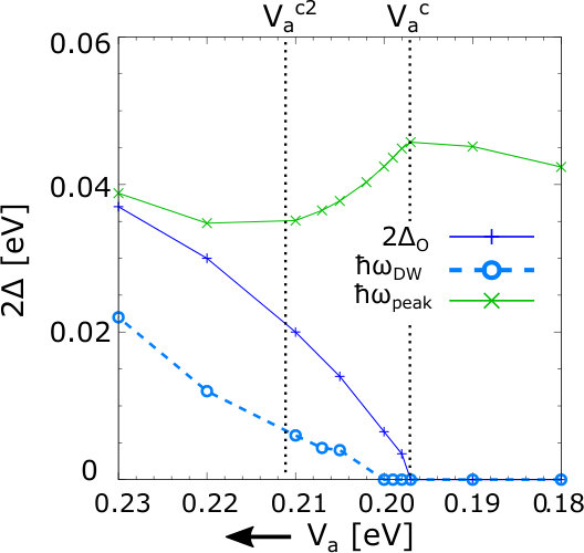 Figure 10
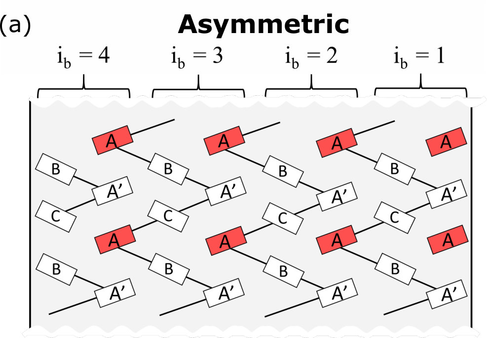 Figure 1
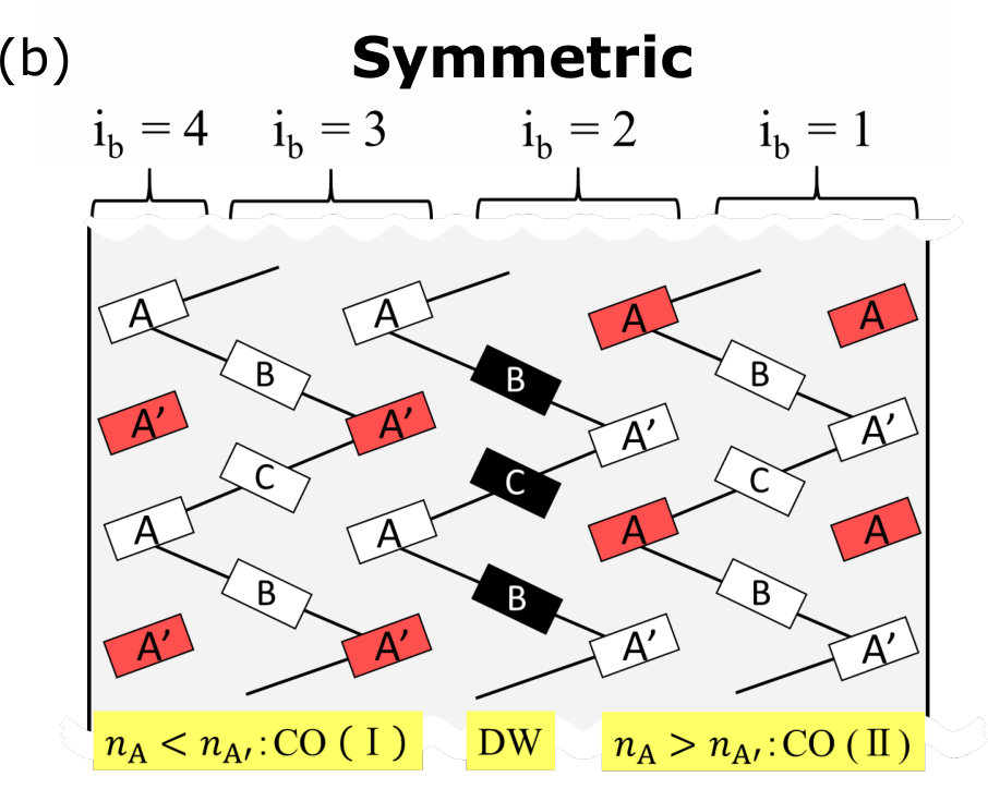 Figure 1
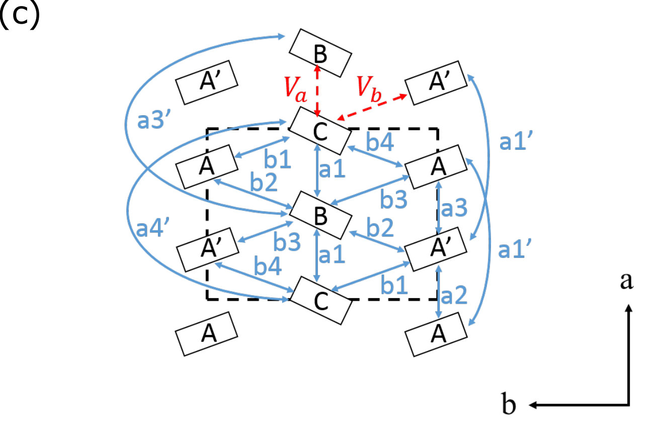 Figure 1
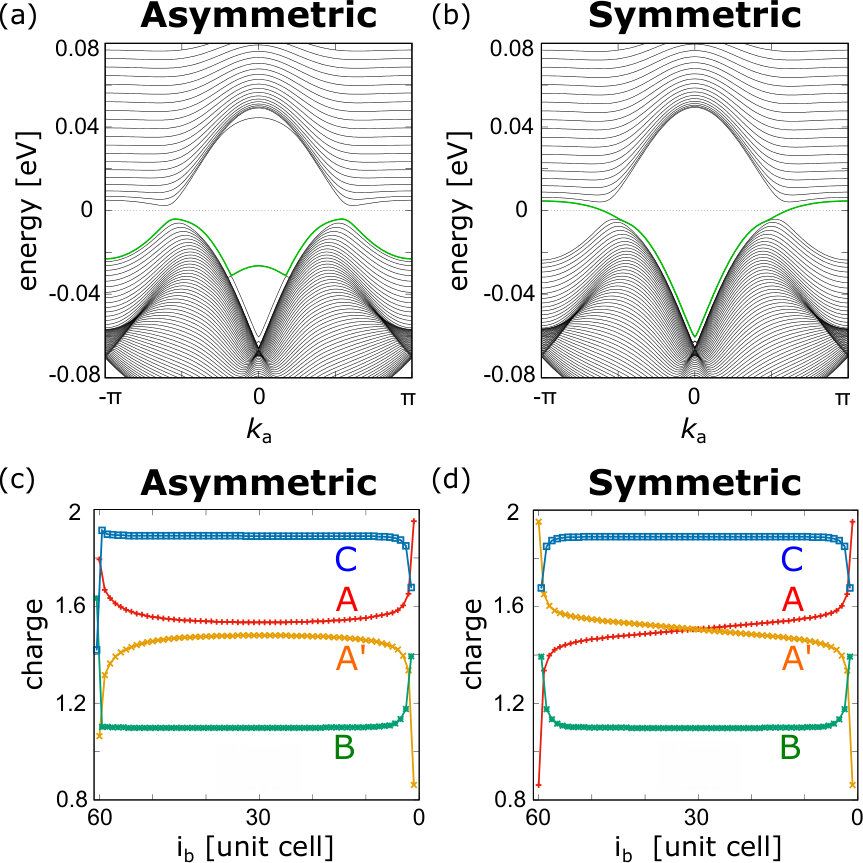 Figure 2
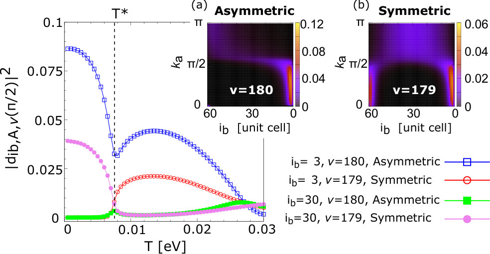 Figure 3
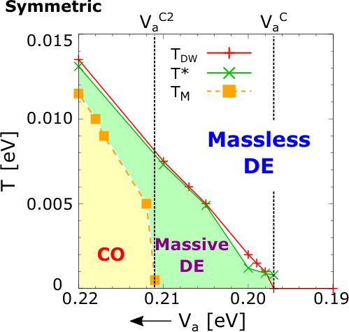 Figure 4
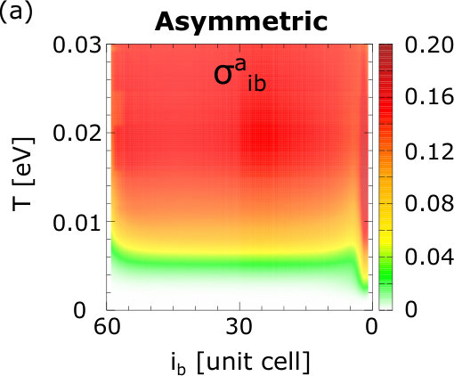 Figure 5
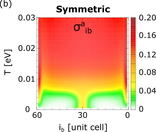 Figure 5
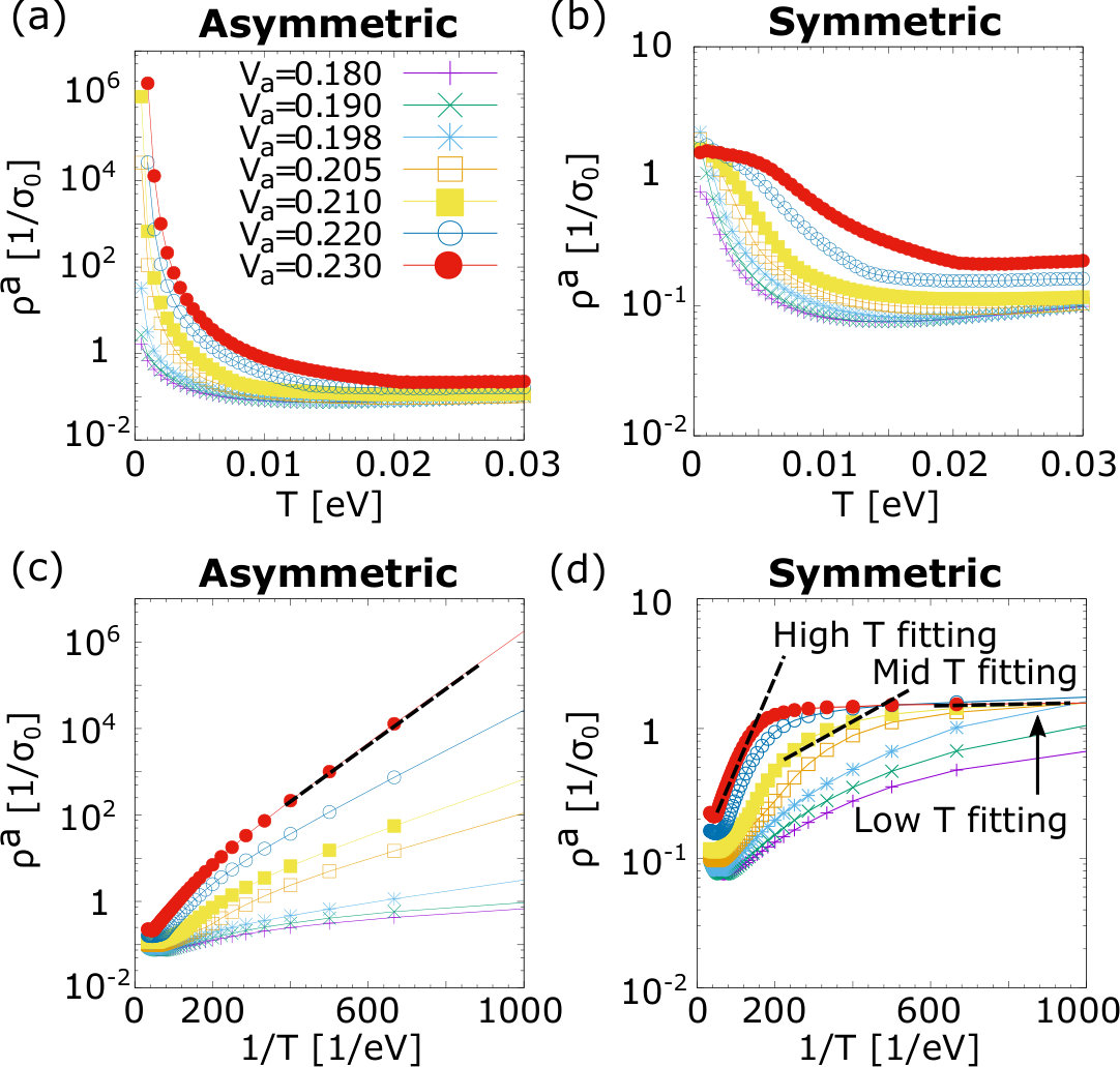 Figure 6
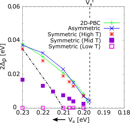 Figure 7
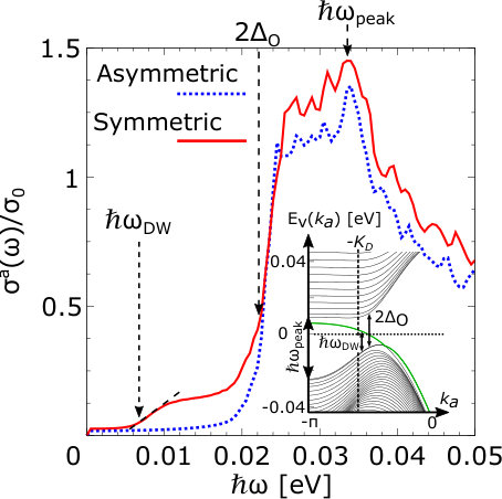 Figure 8
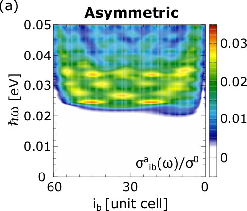 Figure 9
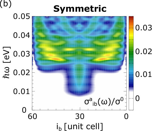 Figure 9
Peer Reviews
No public reviews on file for this paper yet. If you reviewed it on a platform where reviews are public (OpenReview, ICLR, NeurIPS, ICML), you can paste yours below so the community can read it here.
Videos
No videos yet. Explain this paper in a talk, walkthrough, or lecture? Add one.
Domain Wall Conductivity with strong Coulomb interaction of two-dimensional massive Dirac Electrons in the Organic Conductor -(BEDT-TTF)2I3
D. Ohki1
Y. Omori2
A. Kobayashi1
1Department of Physics, Nagoya University, Furo-cho, Chikusa-ku, Nagoya, 464-8602 Japan
2Toyota College, National Institute of Technology, Eisei-cho 2-1, Toyota, 471-8525 Japan
Abstract
Motivated by the results of recent transport and optical conductivity studies, we propose a semi-infinite two-dimensional lattice model for interacting massive Dirac electrons in the pressurized organic conductor -(BEDT-TTF)2I3, and address the problem of domain wall conductivity in a charge-ordered insulating phase under realistic experimental conditions. Using the extended Hubbard model at a mean field level, we present results of extensive numerical studies around the critical region of the model, reporting on the resistivity and optical conductivity calculated by means of the Nakano-Kubo formula. We find that the activation gap extracted from the resistivity data can be much smaller than the optical gap in the critical region, which is induced by metallic conduction along an one-dimensional domain wall emerging at the border of two charge-ordered ferroelectric regions with opposite polarizations. The data are consistent with the observed transport gap in real -(BEDT-TTF)2I3 samples that is reduced remarkably faster than the optical gap upon suppressing charge order with pressure. Our optical conductivity also reveals an additional shoulder-like structure at low energy inside the gap, which is argued to be directly relevant to the metallic bound states residing on the domain wall.
††preprint: APS/123-QED
I Introduction
The quasi-two-dimensional (quasi-2D) electron system in the layered organic salt -(BEDT-TTF)2I3 has a unique pressure-temperature (-) phase diagram in which a 2D massless Dirac electron phase appears at high [1, 2, 3, 4, 5, 6, 7] which an insulating phase is stabilized at low showing charge ordering. In the high- phase the space and time inversion symmetry guaranties the stability of the (spin-degenerate) Dirac points in the momentum space, and the 3/4-filling of the electronic band fixes the Fermi energy at the band-crossing points. In contrast, the inversion symmetry is spontaneously broken in the low- insulating phase where electrons are localized and form a stripe-type charge-ordering pattern along the crystalline axis [8, 9, 10, 11]. At ambient pressure the charge-ordered phase appears below a transition temperature of K. An application of a hydrostatic pressure linearly reduces and eventually suppresses the phase transition above a critical pressure P_{\rm c}{\color[rgb]{0,0,0}\simeq}12 kbar, stabilizing the massless Dirac electron phase at low temperature.
A narrow energy bandwidth characteristic for this type of organic conductors gives rise to strong electronic correlation effects in both phases [1, 2, 12]. As theoretically predicted and also experimentally confirmed, the electron-electron Coulomb interaction plays a significant role in the stripe-type charge-ordered phase at low-. For example, recent NMR and Monte Carlo studies point to a spin-excitation nature that is consistent with one-dimensional (1D) alternating Heisenberg spin chains [8, 9, 13, 14]. Moreover, a novel charge-ordered phase accompanied by massive Dirac electrons has been predicted in the vicinity of the critical region of the phase diagram (), which is induced by the short-range part of the Coulomb interaction (This charge-ordered massive Dirac electron phase can be distinguished from the ordinary charge-ordered phase at lower in terms of the valley Hall effect since the former has a finite valley Chern number, whereas the latter has none [4, 5, 19, 20, 21, 22, 23, 15, 16, 17, 18]). In the high- massless Dirac electron phase, not only the short-range repulsive interactions but also the long-range part of the Coulomb interaction (appearing due to the absence of metallic screening at the Dirac point) induce various anomalies in the NMR spin susceptibilities: A ferrimagnetic spin polarization, a logarithmic suppression of the Knight shift, and orders of magnitude enhancement of the Korringa ratio [24, 25]. Moreover, at low temperature signatures of inter-valley excitonic spin fluctuations were reported as a precursor to the excitonic transition by the long-range part of the Coulomb interaction [24, 26, 25, 27].
Recently, a surprising transport property under pressure has been reported by resistivity measurements [28]. The transport gap estimated by Arrhenius plots turns out to have a much smaller value compared to the optical gap extracted from optical conductivity measurements [29]. The resistivity gap is strongly suppressed as pressure is increased and becomes zero at kbar while and the optical gap remain finite until the pressure reaches . As a candidate of a possible dc conduction mechanism in this critical region ( kbar ), a 1D conduction scheme has been predicted along a gapless bound state on a domain wall formed between two kinds of charge-ordered domains with different polarization [15, 16, 17]. Interestingly, the charge ordering in -(BEDT-TTF)2I3 is also found to be accompanied by ferroelectricity [30, 31, 32] as well as polar domains having a domain size of several hundred micrometers [31]. However, it remains unclear how the formation of these domain walls is related to the observed contrasting pressure dependence of and . To construct a realistic theory in this critical region, one is therefore motivated to start with a minimal model that has a single domain wall formed between two ferroelectric domains possessing opposite electric polarization.
In this paper we develop a numerical approach which accounts for the distinct pressure dependence of and in the pressurized -(BEDT-TTF)2I3, using a cylindrical boundary condition that naturally introduces a domain wall in a space-dependent mean-field theory [33, 34, 15, 16, 17]. The interaction between electrons is treated within the extended Hubbard model, where the canonical on-site interaction and the nearest-neighbor interactions are included. In our recent mean-field studies with semi-infinite [15, 16, 17] and 2D periodic [18] boundary conditions, indications were found that the influence of pressure can be parametrized by the strength of the nearest-neighbor Coulomb interaction along the crystalline axis , which varies most sensitively upon changing the applied external pressure [35, 36] and plays dominant roles in stabilizing the stripe-type charge order [9]. Following this hypothesis, we utilize as our control parameter in this study. Periodic boundary conditions are considered in the direction but edges are placed in the direction to introduce a domain wall in the model. We present extensive numerical calculations of the dc resistivity and the optical conductivity using the T-matrix approximation combined with the Nakano-Kubo formula [37, 38, 39, 40, 16, 18]. This approach provides us a novel way to understand the anomalous behavior of the experimentally reported transport and optical gaps (\Delta_{\rm\rho}{\color[rgb]{0,0,0}\ll}\Delta_{\rm O} around kbar [28, 29]) by domain wall conduction along the direction in the model’s critical region. We also find an unexpected shoulder-like structure in the optical conductivity at low energy, which is discussed in terms of a 1D metallic bound state on the domain wall.
The remainder of this paper is organized as follows. In Sec. II. A, we lay out the extended Hubbard model for -(BEDT-TTF)2I3 subjected to two kinds of cylindrical boundary conditions either symmetric or asymmetric in the direction [15, 16, 17]. We also present a summary of earlier works in this section, putting particular emphasis on geometrical mechanisms behind the formation of a single domain wall and showing its energy spectrum. In Sec. II. B, we present the formalisms of dc and optical conductivities within the T-matrix approximation using the Nakano-Kubo formula. Details of their formulations are summarized in Appendix A. Our numerical results are shown in Sec. III. In Sec. III. A, we first focus on the temperature dependence of the spatially-resolved electronic states for the two types of boundary conditions with and without a domain wall. We also present the interaction-temperature (-) phase diagram which, for the symmetric-edge case, confirms the presence of a domain wall in a wide parameter region in the charge-ordered phase. In Sec. III. B, results for the temperature dependent dc resistivity are shown for various sizes of , in which Arrhenius fits to the data reveal a transport gap that is strongly dependent on the fitted temperature range. In Sec. III. C, we evaluate the optical conductivity as a function of energy and boundary types, which provides the optical gap for a range of interaction sizes. We summarize our findings for the domain wall conduction in Sec. VI and also try to associate our proposed conduction mechanism to the results in real -(BEDT-TTF)2I3 by considering realistic experimental and materialistic conditions.
II Model and Formulation
II.1 Models and Summary of Previous Studies: Emergent Domain Wall by Geometrical Constraints
Before presenting the main results of this paper, let us first introduce our semi-infinite models that require special cares on the treatment of edges. We then proceed to show the Hamiltonian and summarize previous key findings derived from these models; in particular, we focus on the geometry-necessitated mechanism of domain wall formation between two different charge-ordered domains [15, 16, 17].
To begin with, the model we rely on aims to describe conduction mechanisms in -(BEDT-TTF)2I3 in a realistic situation where cylindrical boundary conditions are employed in the conducting 2D plane. More specifically, we assume a periodic boundary condition along the crystalline axis, whereas edges are introduced along the axis, as presented in Figs. 1(a) and (b). The 2D unit cell in the (low-) charge-ordered state contains four nonequivalent molecular sites (dubbed A, A*′, B and C) [12, 41] which form two distinct columns in the direction, labeled as AA′* and BC (see Fig. 1). Because of these two column types, there are three ways to introduce edges at the two ends in the direction: AA*′-AA′, AA′-BC and BC-BC. Among these, AA′-AA′* and BC-BC have symmetric edges and lead to similar results within this theory. Therefore, we will not distinguish them hereafter and will only focus on the two edge types of AA*′-BC and AA′-AA′* that are either asymmetric (AA*′-BC) [Fig. 1(a)] or symmetric (AA′-AA′*) [Fig. 1(b)] in the direction.
The electronic structure in -(BEDT-TTF)2I3 is somewhat involved due to a complicated 2D inter-molecular network of hopping integrals. Figure 1(c) shows the nearest and next-nearest neighbor hoppings in the conducting phase used in this study, where the system has inversion centers between the molecules A and A*′* as well as on the molecules B and C [11]. Note that the sizeable hopping integrals [in particular b1 and b2 in Fig. 1(c)] form a zigzag network along the direction [shown by solid lines in Figs. 1(a) and 1(b)].
As we reported previously, the molecules at the edges residing off these zigzags are close to charge neutral (i.e., closed shell), whereas the other molecules residing on the zigzags are positively charged reflecting the hole 1/4 filling (electron 3/4 filling) of the electronic bands [16]. That kind of charge neutral molecules isolated from the zigzags appear only in the AA*′* column locating at the edges; for the (AA*′-AA′) symmetric-edge pattern, the isolation occurs at the molecule A on one edge while it takes place at the molecule A′* on the other [Fig. 1(b)]. Because of this and the fact that the charge carriers (i.e., holes) are localized either on the molecule A or A*′* (plus B) in the strip-type charge-ordered state [11], the (AA*′-AA′) symmetric-edge pattern inevitably acquires at least one domain wall on a BC column necessitated by the geometry [16] [Figs. 1(b) and 2(d)]. For the (AA′-BC) asymmetric-edge pattern, by contrast, no domain walls are required as there is only one AA′* column at an edge, and the charge-ordering pattern can be uniquely determined [Fig. 1(a)]. Generally speaking, charge-ordered domains are accompanied by spontaneous electric polarization [30, 31], causing multiple domain walls at the boundaries of several ferroelectric domains, as is the case for conventional ferroelectric materials. To make the story simple, however, we will omit these additional domain walls in this study and concentrate only on the one required from the geometrical arguments.
Next, so as to the Hamiltonian, we consider a 2D Hubbard-type model serving as a standard framework to study interacting electrons on a lattice. In the orthodox Hubbard model one only considers a repulsive on-site interaction between electrons of opposite spin, but in this study we incorporate the nearest-neighbor interactions playing one of the most essential roles in driving the charge-ordering transition in -(BEDT-TTF)2I3, as theoretically suggested [9] and experimentally confirmed by NMR [14]. We also introduce edge potentials following Ref. [16] to treat the effects of surface charge recombination. (In addition, we note that the interactions between BEDT-TTF molecules and I3 anions would also play some roles in charge order as argued in Ref. [42]. Although we do not exclude that possibility, these interactions are assumed to have only minor influences on our arguments and are thus neglected.) The Hubbard-type model used in this study is described by the Hamiltonian which is given by a sum of the kinetic term
[TABLE]
and the interaction term
[TABLE]
Here, represents a molecule = A, A*′*, B, and C in the -th unit cell, for the space slices in the direction and in the direction , respectively. is the nearest-neighbor or next-nearest-neighbor hopping integral between sites and . is the (molecule-independent) on-site interaction, and represents the nearest-neighbor repulsive interaction between electrons at sites and , for which one can consider two types, dubbed and as shown in Fig. 1(c). () creates (annihilates) an electron of spin at site , stands for the density of electrons with spin at site , and the density at site is summed over all spin projections. Following recent analyses of the high-pressure NMR data [24, 25], we use the values of given by a first principle calculation in Ref. [43]: , , , , , , , , , [in eV; see Fig. 1(c)]. The interaction parameters are set to literature-accepted values eV and eV [15, 16, 17], and, again, is the control parameter of the model. The third term in [Eq. (2)] represents an edge potential that only acts on the electrons residing at the edge sites; following Ref. [16], we assume . The system size is set as and , and a Fourier transformation is performed along the axis using the operator defined for and the wavenumber vector . Within the Hartree approximation we get a mean-field Hamiltonian that is diagonalized in the band representation and has an energy eigenvalue , as described by
[TABLE]
where indicates the band index and is defined using an unitary matrix [which is the eigenfunction in Eq. (4)] as . The charge carrier density at the site is calculated as \langle n_{l_{b}}\rangle=N_{a}^{-1}\sum_{k_{a}\sigma}\sum_{\nu}{\color[rgb]{0,0,0}\left|d_{l_{b}\nu\sigma}({k_{a}})\right|^{2}}\langle c^{\dagger}_{{k_{a}}\nu\sigma}c_{{k_{a}}\nu\sigma}\rangle. Throughout this manuscript, eV is used as the unit of energy.
Finally, let us show that an emergent gapless state naturally appears on the the domain wall in the above model [15, 16, 17]. Figures 2(a) and (b) show the mean-field energy eigenvalue around the Fermi level at the transition temperature to the charge-ordered state (hereafter referred to as ) for the (AA*′-BC) asymmetric- and (AA′-AA′) symmetric-edge patterns, respectively. (Note that is defined from the point where a discontinuous jump occurs in the second derivative of the Helmholtz Free energy .) A gapless energy spectrum arising from the domain-wall bound state crosses for the (AA′-AA′) symmetric-edge [green curve in Fig. 2(b)], whereas there is no gapless states for the (AA′-BC) asymmetric-edge such that the system remains fully gapped [see Fig. 2(a), where the green curve represents the top level in the valence band]. In Figs. 2(c) and (d) the corresponding mean electron density at site is plotted for the (AA′-BC) asymmetric-edge [Fig. 2(c)] and (AA′-AA′) symmetric-edge [Fig. 2(d)] patterns. For the (AA′-AA′*) symmetric case intersects at signifying the appearance of a domain wall. In this study we investigate the temperature dependence of these electronic states, whose detailed nature including the phase diagram has not yet been fully understood.
II.2 Optical Conductivity
In order to evaluate the optical gap, we calculate the optical conductivity given by the following Nakano-Kubo formula
[TABLE]
where is a current-current correlation function in which the Matsubara frequency is analytically connected to a real frequency . The optical conductivity is calculated in a clean limit. In the zero-frequency limit equation (5) gives the longitudinal conductivity along the axis (corresponding to the Drude term) [37, 38, 39, 40, 16]
[TABLE]
where is the Fermi-Dirac function and is a distribution function that is calculated for impurity scatterings using the T-matrix approximation, as expressed by
[TABLE]
Here, is the 2D system size, is an relaxation time and is a velocity derived from a wavenumber derivative of the energy eigenvalue . A spatially resolved conductivity is calculated as
[TABLE]
(For the details of derivations, see Appendix A and Ref [16].) In the following, the conductivity is normalized to the universal conductivity , and the Drude term is subtracted.
III Numerical Results
III.1 Local Electronic Structures and the Massive Dirac Electron Phase
In Fig. 3 we plot the temperature dependence of the modulus of the squared A-site eigenfunction at , , in which we focus on the bands and at the unit cell locating at the center () and around the right end (). (For the definition of these band indices, see the caption of Fig. 2). The 2D plot of at is also shown in the insets, plotted as a function of and for the (AA*′-BC) asymmetric-edge pattern [; inset (a)] and the (AA′-AA′*) symmetric-edge pattern [; inset (b)]. A clear change in the temperature dependence appears at in (open squares) and (filled circles).
For emergent edge states are clearly visible for the both edge patterns, although the amplitude of is twice larger than . Moreover, the edge state appears only at the right end for the (AA*′-BC) asymmetric case [inset (a)], whereas it is visible at both ends for the (AA′-AA′) symmetric case [inset (b)]. These results suggest that the electrons tend to gather more easily around the charge-neutral molecules appearing in the AA′* column of the edges (see Fig. 1).
For a redistribution of electrons takes place for the (AA*′-AA′) symmetric case, shifting electrons from an edge ( at ) to the center ( at ) due to a formation of a domain wall and an associated bound state. For the (AA′*-BC) asymmetric case, by contrast, electrons do not gather around the center, but instead the population around the right edge ( at ) suddenly increases below , signaling that electrons are bound to the charge-neutral molecules at that edge [see Fig. 1(a)]. These edge-bound electrons might contribute to the conductivity by thermal excitations.
Figure 4 shows the interaction-temperature (-) phase diagram for the (AA*′-AA′*) symmetric-edge pattern, where we present three characteristic energy scales: , , and . Already introduced as the metal-to-insulator transition temperature, also defines a phase boundary between the massless Dirac phase (with gapless Dirac cones) and the (charge-ordered) massive Dirac phase (with gapped Dirac cones). , which coincides with , gives the energy scale for forming a single domain wall determined from the temperature where the domain-wall width diverges [15, 17], and represents a merging transition of two gapped Dirac cones [4, 5, 19, 20, 21, 22, 23, 15, 16]. The fact that we have directly supports the notion that the domain wall only appears in the charge-ordered state and disappears in the massless Dirac phase. To have a better understanding of this phase diagram, it is informative to focus on the evolution of the electronic state at low temperature as a function of . As one increases , there is first a transition from the massless Dirac phase to the massive Dirac phase at (at ) occurring simultaneously with the charge ordering [15, 16, 17]. Upon further increasing , the merging transition takes place at (at ) where the system changes from the (charge-ordered) massive Dirac state () to the charge-ordered state with no Dirac cones () (As we mentioned previously, the valley Chern number changes from a finite value to zero across this transition [15], but in both phases metallic bound states exist along the domain wall). The latter critical interaction value well agrees with what is deduced from the previous study using the 2D periodic boundary condition ( at [18]). We note, however, that the real situation is a bit more complicated because the merging happens separately in the conduction and valence bands in -(BEDT-TTF)2I3 reflecting the tilt of the Dirac cones; in Fig. 4 we thus defined from the merging of two energy minima taking place in the conduction band.
III.2 Temperature Dependence of the Resistivity and the Transport Gap
Next, we calculate the temperature dependence of the resistivity to estimate the transport gap . Figures 5(a) and (b) present the 2D plots of the spatially resolved dc conductivity in the direction (at ) plotted as a function temperature and the position in the direction for the (AA*′-BC) asymmetric-edge pattern [Fig. 5(a)] and the (AA′-AA′) symmetric-edge pattern [Fig. 5(b)]. The plots reveal a very different nature in the low behaviors for two cases. For the (AA′-BC) asymmetric pattern, vanishes at low in the bulk of the sample since a gap opens at the Fermi energy. For the (AA′-AA′) symmetric pattern, by contrast, becomes vanishingly small at low except for the central region of the sample (i.e., ) where a gapless 1D bound state appears on the domain wall [Fig. 2(b)] and yields finite conductivity [16]. Note that high conductivity also survives at low on the two edges in the (AA′-AA′) symmetric case, whereas it remains large only on the right end in the (AA′*-BC) asymmetric case (for ). These high conductivities can be explained by thermal edge conductance owing to the edge-bound electrons, as we mentioned in the previous section (see Figs. 2 and 3).
To have a closer look on the temperature dependence, we measured the dc resistivity as a function of in the direction for several strengths of interaction ranging from 0.180 to 0.230. The resulting curves for the (AA*′-BC) asymmetric- and (AA′-AA′) symmetric-edge patterns are shown in Figs. 6(a) and 6(b), respectively. For the (AA′-BC) asymmetric pattern [Fig. 6(a)], the curves start to diverge at low above the critical interaction . This divergence signals the opening of a gap via spontaneous charge ordering, in line with our recent results using the 2D periodic boundary condition [18]. These data are contrasted to the (AA′-AA′) symmetric pattern [Fig. 6(b)] in which the resistivity does not diverge but levels off at low for since the domain-wall formation in the charge-ordered state results in a finite conductivity along the gapless bound state [Fig. 5(b)]. The values of the resistivity gap can be extracted from exponential fits to the Arrhenius plot of , presented in Figs. 6(c) and 6(d) for the (AA′-BC) asymmetric- and (AA′-AA′) symmetric-edge patterns, respectively. Upon increasing , the slope of the data shows a systematic increase for in the (AA′-BC) asymmetric case [Fig. 6(c)], pointing to a continuous evolution of as a function of . For the (AA′-AA′*) symmetric case [Fig. 6(d)], however, the curves of show a nonmonotonic behavior as one increases ; for large values of there is a steep slope at high (around the transition temperature ), a gradual increase at intermediate (), and a clear levelling-off at low (\simeq 0.001{\color[rgb]{0,0,0}\ll}T^{*}). These contrasting behaviors yield different estimates of in the charge-ordered state () that strongly depend on the range of the fits to the data, as we shall see below.
We note here that the calculated curves of in Fig. 6(d) have many features in common with the recent experimental data at a range of pressure [28], showing strongly nonmonotonic changes in the shape of upon increasing . This apparent similarity motivates us to make a comparison of the calculated values of with the experimentally obtained , considering instead of as a control parameter of the charge-ordering transition. To this end, we perform fits using different fitting ranges to Figs. 6(c) and 6(d). Figure 7 plots the resulting values of against for several fitting procedures. The horizontal axis is reverted to make a comparison to the pressure-dependence data in Ref. [28]. The charge-ordering gap starts to open at and continues to develop almost linearly for . For the (AA*′-BC) asymmetric pattern the gap size agrees with that for the 2D periodic boundary condition [18] since the bulk appearance of charge order results in a unique definition of the gap. In contrast, the evolution of for the (AA′-AA′*) symmetric pattern shows a marked difference for certain types of fits. The fits at high yield a similar result to the above two cases, pointing to a small influence of the domain-wall bound state at high temperature. On the other hand, the gap becomes smaller for the intermediate- fits and is almost zero for the low- fits, reflecting the presence of the metallic bound state dominating the conductivity at low temperature.
In Ref. [28] the authors examined fits to the Arrhenius plot of experimental resistivity at various values of for determining , but their choice of fitted temperature range varies from pressure to pressure: (i) At ambient pressure the fit was performed just below the transition temperature (High ), (ii) for and kbar it was done at half of the transition temperature (Mid ), and (iii) for kbar it was done at a low-temperature limit below 20 K (Low ). Given the similarity of the experimental Arrhenius plot and Fig. 6 (d), one is tempted to hypothesize that there is a correspondence between the -dependent choice of the fitted temperature range in [28] and the -dependent fit range in Fig. 6(d). By doing so, we are able to estimate an expected curve of corresponding to the experimental data (indicated by the black dash-dotted line in Fig. 7).
III.3 Optical Conductivity and Optical gap
As a next step, we calculated the optical conductivity in the direction for the (AA*′-BC) asymmetric- and (AA′-AA′) symmetric-edge patterns, where the interaction was varied between 0.180 and 0.230. The representative conductivity data normalized to deep in the charge-ordered phase (at and ) are presented in Fig. 8. The overall shape of the optical conductivity spectra is more or less similar for the two edge patterns and is characterized by two energy scales, and . A sharp drop at meV signals the opening of a direct charge-ordering gap at the Dirac point. Above the gap, there is a hump-like structure with a peak at meV. The peak is ascribed to a direct transition between different van Hove singularities in the conduction and valence bands, locating at a time reversal invariant momentum (TRIM). Similar structures have been observed in the previous study using the 2D periodic boundary condition [18]. A remarkable difference found in the present cylindrical model is the additional bump at low energy with a kink at meV, which only appears for the (AA′-AA′*) symmetric pattern. This bump can be associated to a direct transition between the valence band and the gapless band at the Fermi energy linked to the 1D bound state on the domain wall. In addition, we note that is almost half the charge-ordering gap since the Fermi energy locates at approximately the mid point of the gap (for details, see the inset of Fig. 8).
Figures 9(a) and 9(b) show the 2D plots of the spatially resolved optical conductivity normalized to in the charge-ordered phase (at ) calculated at for the (AA*′-BC) asymmetric-edge pattern [Fig. 9(a)] and the (AA′-AA′) symmetric-edge pattern [Fig. 9(b)], plotted as a function of and the position in the direction. A spatially uniform optical gap is clearly visible in both plots except for the central region () in Fig. 9(b) where the conductivity increases from a lower energy due to the domain-wall bound state, bringing about a T-shaped structure. At the edges finite conductivity resumes due to a direct transition between the edge states (Fig. 3) and the conduction band. The edge conductance is absent at the left edge () for the (AA′*-BC) asymmetric pattern in Fig. 9(a) since there is no edge states in this case.
In Fig. 10 we present results for the optical gap and the two characteristic energy scales, and (The horizontal axis is inverted to make a comparison with the transport gaps in Fig. 7). The results of and show identical behaviors for the (AA*′-BC) asymmetric and (AA′-AA′*) symmetric patterns and will not be distinguished. The optical gap approximately increases linearly with increasing , which is paralleled by that also linearly develops in a similar fashion. Note that the magnitude of is about 50 the size of as we mentioned above. By contrast, is almost flat at lower , starts to decrease at (due to a deformation of energy bands at the charge-ordering transition [18]), gradually approaches for , and eventually becomes almost identical to for . The last point agrees with the fact that the van Hove singularities in the conduction and valence bands disappear when the merging transition occurs at since in that case direct transitions between the singular points also vanish. We have reported similar asymptotic behaviors of and for the 2D periodic boundary condition in Ref. [18]. This similarity suggests that the overall changes of the band topology and the optical gap are irrespective of boundary choices (i.e., the absence or presence of a domain wall).
IV Summary and discussion
In this study we examined the detailed temperature dependence of the electronic states of interacting 2D Dirac electrons in -(BEDT-TTF)2I3 by using a minimal lattice model at a mean-field level. More specifically, we assumed cylindrical boundary conditions that, depending on the type of edges, necessitate a single domain wall as a consequence of geometrical constraints. An interaction-temperature (-) phase diagram is proposed which we claim to correspond to the experimentally-reported pressure-temperature (-) phase diagram if one associates an increase in with a reduction in .
We find clear evidence for a formation of a domain wall in the entire charge-ordered phase () for the (AA*′-AA′) symmetric-edge pattern. The key finding is the discovery of a conduction mechanism along the 1D domain-wall bound state that excellently explains the experimental discrepancy in the sizes of transport and optical gaps under pressure. The conduction along this bound state turns out to offer a major contribution to the transport conductivity at large , whose degree increases upon cooling and completely dominates the conduction at low temperature, resulting in a saturation of resistivity and a vanishingly small transport gap. In contrast, the impact of the bound state is rather limited in the optical conductivity, giving rise to a finite gap in the optical spectra regardless of the size of in the charge-ordered phase [The bound state causes, however, a small additional bump at low energy () corresponding to an in-gap bound state]. As a direct consequence of these differences, the transport gap ends up with a vanishingly small value at low temperature, whereas the optical gap stays finite, in a remarkable agreement with the experiments. We therefore conclude that the emergent domain wall must be relevant to the observed discrepancy in the experimental gap sizes. This point is in line with our supportive calculations using the (AA′*-BC) asymmetric-edge pattern and the 2D periodic boundary condition since in these cases there is no domain wall, and the two gaps reasonably coincide.
We also demonstrate that the Arrhenius analyses of the resistivity data provide unusual gap values for large depending strongly on the slice the data are fitted. The gap is identical to the bulk gap just below the transition temperature , whereas it is largely suppressed towards lower and eventually becomes zero at low . We reiterate that a very similar behavior has been reported in the recent transport experiments under pressure; Fig. 1(b) of Ref. [28] highlights at low a levelling-off-like feature of resistivity developing upon increasing pressure, which draws an excellent parallel with the calculated resistivity in Fig. 6(d) showing a similar saturation at large . This strongly reinforces our original hypothesis that the major impact of pressurization is altering the size of .
Of course our assumption in this model is somewhat oversimplified, and in reality pressure would also changes other parameters such as the electronic bandwidth as well as interactions between BEDT-TTF molecules and I3 anions [42]. In our view, however, these effects are insufficient to qualitatively reproduce the remarkable saturation of low- resistivity, allowing us to safely omit these effect as a first approximation. Unfortunately, the putative model we rely on precludes us from making a more quantitative analysis of the gap sizes at this stage. In this regard a more complete calculation considering all these pressurization effects may prove interesting.
The finding of the phase diagram also reveals that the charge-ordered phase is divided into two subgroups in an extended region on the - plane; namely, the massive Dirac electron phase with gapped Dirac cones on the lower-interaction side () and the trivial charge-ordered phase without any cone on the higher-interaction side (). The categorization of these two phases in terms of the valley Hall effect would be informative for improving further understanding of charge order in this material.
We note that while our model assumes semi-infinite boundary conditions and is hence different from the situation in naturally grown -(BEDT-TTF)2I3 bulk samples, a real crystal is a quasi-2D material consisted of a multiple stacks of 2D conducting layers which inevitably has edges in each layer of either (AA*′-BC) asymmetric- or (AA′-AA′) symmetric-edge patterns. Taking proper account of this, one can expect that at least certain portions of the layers are comprised of the (AA′-AA′*) symmetric-edge pattern. We therefore argue that the domain-wall conductance must be relevant at low temperature as long as these symmetrically edged layers are concerned. Recent experimental reports on the electronic ferroelectricity in -(BEDT-TTF)2I3 at ambient pressure [30, 31, 32] agree with this notion, which point to the presence of multiple domain walls created between charge-ordered regions having opposing electric polarizations. Another interesting remark is that the saturation-like behavior of resistivity emerges even at ambient pressure in some samples [14] (albeit it is absent in others [28, 44]). For real materials this suggests that the domain wall conduction may be present in a much wider region in the charge-ordered phase. We propose that optical conductivity or real-space resolved spectroscopy would be able to confirm domain walls, which should see some bump structures at low energy inside the charge-ordering gap.
Finally, let us recall that our mean-field theory assumes a minimal model which only considers a single domain wall necessitated by geometrical requirements (i.e., the type of edges at the two ends in the direction). To go one step ahead, one should take, for instance, thermal effects into account which can cause excitations of multiple domain walls by fluctuations. Nevertheless, we believe that the qualitative features of the transport and optical gaps, in particular their discrepancy in size, would not be altered much by the presence of excess domain walls. In that regard, our arguments are expected to be durable even in the presence of fluctuations, although further studies are clearly needed for gaining deeper insight into these phenomena. It will be an interesting future problem to consider the creation and annihilation of domain walls as well as their dynamic properties.
Acknowledgements.
The authors would like to thank S. Onari, K. Miyagawa, K. Kanoda, and H. Fukuyama for fruitful discussions, and Y. Yamakawa for advice on numerical calculation. We would also like to express our gratitude to M. Hirata for discussions as well as reading and correcting the manuscript. This work was supported by MEXT/JSPJ KAKENHI under Grant Nos. 15K05166 and 19J20677.
Appendix A Details of the formulation in the cylindrical systems using extended Hubbard model
In Appendix A we introduce the detailed formulations used in this study. Our starting point is a Hamiltonian which is described in the site representation [see equations (1) and (2) in the main text]. Making a Fourier transformation along the axis, we define the Fourier inverse transform for site (-th unit cell in the direction and -th molecule) and wavenumber vector . The Hamiltonian in the wavenumber representation then reads
[TABLE]
Here, and are defined as and , respectively, with a momentum transfer and a vector connecting all possible-nearest neighbor sites. Within the Hartree approximation one obtains a mean-field Hamiltonian
[TABLE]
where is the mean density of electrons with spin at site averaged for the Fermi distribution. Diagonalization of leads to the energy eigenvalue and the eigenfunction , which results in a formation of the energy bands for the (AA*′-AA′) symmetric-edge ((AA′*-BC) asymmetric-edge) pattern. Recalling the orthogonality , the Hamiltonian becomes
[TABLE]
with . The chemical potential is determined from the quarter filling condition . Note that we set . Using Eqs. (A6) and (A7), we will evaluate the electronic properties at finite temperature, in particular the optical and dc conductivities.
The optical conductivity along the axis is calculated by the Nakano-Kubo formula which is formulated in terms of a linear response theory, given by
[TABLE]
where is the 2D system size and is the Fermi-Dirac distribution function.
The longitudinal dc conductivity [37, 38, 39, 40, 16] along the axis is given by
[TABLE]
where we introduced velocity variables
[TABLE]
The retarded Green’s function is expressed in the T-matrix approximation as
[TABLE]
with the retarded self-energy
[TABLE]
and the single-particle retarded Green’s function
[TABLE]
Here, we defined the impurity potential
[TABLE]
for the number of impurity centers and the density of impurities in the direction. The damping constant is given by the imaginary part of and is calculated as
[TABLE]
where is a site-resolved spectral density given by
[TABLE]
Recalling that defines the relaxation time, one is able to simplify in Eq. (A11) as follows:
[TABLE]
To see the spatial distribution of conductivities along the direction, a spatially-resolved conductivity is defined by
[TABLE]
with a spatially-resolved distribution function
[TABLE]
The dc conductivity (or the dc resistivity ) is derived from a summation of over all possible in the direction.
The reference list from the paper itself. Each links out to its DOI / PubMed record.
- 1[1] K. Kajita, T. Ojiro, H. Fujii, Y. Nishio, H. Kobayashi, A. Kobayashi, and R. Kato, J. Phys. Soc. Jpn. 61 , 23 (1992).
- 2[2] N. Tajima, M. Tamura, Y. Nishio, K. Kajita, and Y. Iye, J. Phys. Soc. Jpn. 69 , 543-551 (2000).
- 3[3] A. Kobayashi, S. Katayama, K. Noguchi, and Y. Suzumura, J. Phys. Soc. Jpn. 73 , 3135 (2004)
- 4[4] S. Katayama, A. Kobayashi, and Y. Suzumura, J. Phys. Soc. Jpn. 75 , 054705 (2006).
- 5[5] A. Kobayashi, S. Katayama, Y. Suzumura, and H. Fukuyama, J. Phys. Soc. Jpn. 76 , 034711 (2007).
- 6[6] M. O. Goerbig, J.-N. Fuchs, G. Montambaux, and F. Pi e ´ ´ e \acute{{\rm e}} chon, Phys. Rev. B 78 , 045415 (2008).
- 7[7] K. Kajita, Y. Nishio, N. Tajima, Y. Suzumura, and A. Kobayashi, J. Phys. Soc. Jpn. 83 , 072002 (2014).
- 8[8] H. Kino and H. Fukuyama, J. Phys. Soc. Jpn. 64 , 4523 (1995).