A simple rule for finding Dirac Cones in Bilayered Perovskites
XueJiao Chen, Lei Liu, DeZhen Shen

TL;DR
This paper introduces a straightforward rule to identify Dirac cone electronic states in bilayered perovskites by focusing on active atom groups, demonstrated through DFT calculations on specific materials, revealing high Fermi velocities and potential for ultra-fast devices.
Contribution
The paper presents a simple, general rule for locating Dirac cones in bilayered perovskites based on quasi-atom lattices, validated with DFT calculations.
Findings
Both bilayers exhibit Dirac cones near the Fermi level.
Fermi velocities reach approximately 0.2×10^6 m/s.
The materials are promising for ultra-fast electronic devices.
Abstract
We propose a simple rule for finding Dirac cone electronic states in solids, that is neglecting those lattice atoms inert to the particular electronic bands, and pursuing the two dimensional (2D) graphene-like quasi-atom lattices with s- and p-bindings by considering the equivalent atom groups in the unit cell as quasi-atoms. With CsPbBr and CsBiBr bilayers as examples, we demonstrate the effectiveness and generality of this rule with the density functional theory (DFT) calculations. We demonstrate that both bilayers have Dirac cones around the Fermi level and reveal that their corresponding Fermi velocities can reach as high as 0.210m/s. That makes these new 2D layered materials very promising in making new ultra-fast ionic electronic devices.
Click any figure to enlarge with its caption.
 Figure 1
 Figure 2
 Figure 3
 Figure 1
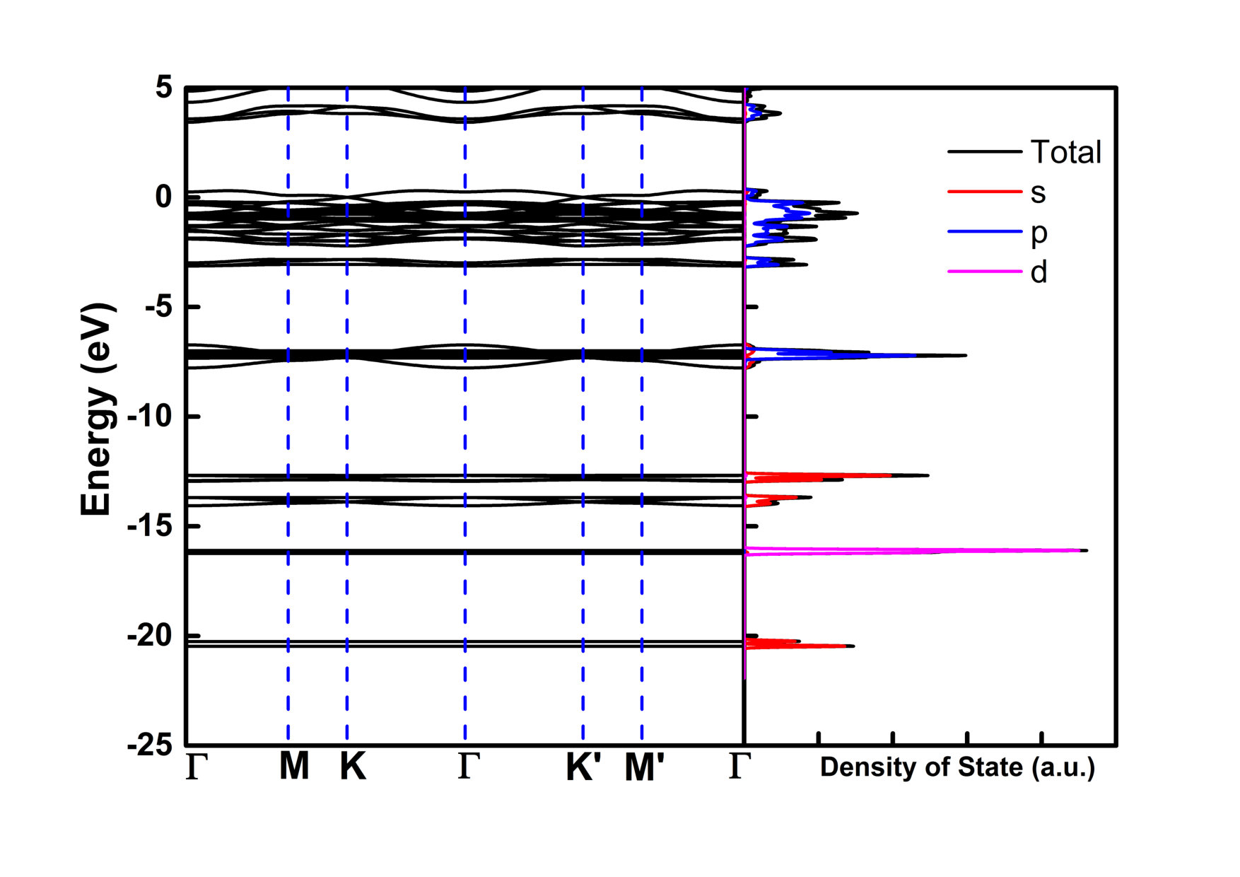 Figure 2
Peer Reviews
No public reviews on file for this paper yet. If you reviewed it on a platform where reviews are public (OpenReview, ICLR, NeurIPS, ICML), you can paste yours below so the community can read it here.
Videos
No videos yet. Explain this paper in a talk, walkthrough, or lecture? Add one.
Abstract
We propose a simple rule for finding Dirac cone electronic states in solids, that is neglecting those lattice atoms inert to the particular electronic bands, and pursuing the two dimensional (2D) graphene-like quasi-atom lattices with s- and p-bindings by considering the equivalent atom groups in the unit cell as quasi-atoms. With CsPbBr and CsBiBr bilayers as examples, we demonstrate the effectiveness and generality of this rule with the density functional theory (DFT) calculations. We demonstrate that both bilayers have Dirac cones around the Fermi level and reveal that their corresponding Fermi velocities can reach as high as 0.2106m/s. That makes these new 2D layered materials very promising in making new ultra-fast ionic electronic devices.
“Dirac Cone”, describing the gapless linear-dispersion of electronic bands, characterizes the superior ballistic massless charge-carrier transport of solids such as in graphene Wallace (1947); Novoselov et al. (2005); Zhang et al. (2005), or on the surfaces of topological insulatorsBernevig et al. (2006); Hsieh et al. (2008); Chen et al. (2009). Theoretically, the Dirac cones had been predicted in 1947 in graphene, whose honeycomb lattice of - bonding results in the conical band structure with the linearly dispersive valence and conduction bands touching each other at the Dirac points (K or K*′*) of its hexagonal Brillouin zoneWallace (1947). Nevertheless, it was only after its first isolationNovoselov et al. (2004), graphene has become a source of new sciences, and aroused research upsurges again and again over its novel electronic behaviorsGeim and Novoselov (2007); Geim (2009); Castro Neto et al. (2009); Brumfiel (2009); Service (2009); Nat (2010); Kim (2010); Novoselov et al. (2012); Service (2015); Gibney (2018); Cao et al. (2018). In fact, by energy-band theory and symmetry analysisWallace (1947), the normal Dirac cones as presented in graphene will generally appear in those materials, as long as they have the similarly honeycomb bonding style as graphene does. But, among hundreds of 2D materials examined by now, only graphynesMalko et al. (2012), silicene and germaneneCahangirov et al. (2009), ionic boronMa et al. (2016), and othersWang et al. (2015) have been identified to be the normal Dirac materials. Nevertheless, unlike graphene, these 2D Dirac materials are made of some sort of artificial lattices where the atoms do not bond together as they do in their stable natural structural polymorphs. In this letter, we propose that following a simple but effective rule more Dirac cone states can be found generally in the 2D materials with stable natural bonding structures.
Here, perovskites are selected to demonstrate physics behind the rule we proposed for finding 2D Dirac materials. As shown in Fig. 1a, normally perovskites have the well-known ABX lattice structure, where the 6-fold coordinated B cation and its surrounded X anions form the BX octahedron, the BX octahedra share their X corners forming the 3D skeleton, and the A cations occupy every hole among the 8 BX octahedra. For a cubic ABX lattice, if viewed from the [111] direction, it presents natively the hexagonal symmetry as shown in Fig. 1b. While the A cations stay isolated from the BX skeleton, their electronic states normally do not participate in forming the low-energy bands dispersing near the Fermi level. For a selected halide perovskite (CsPbBr), Fig. 1c plots its gapped electronic band structure calculated with DFT, together with the total and site-decomposed density of states (DOS). That demonstrates clearly that the electronic orbitals of the A cations stay a few electronvolts away from the valence band maximum (VBM) and the conduction band minimum (CBM) and thus play no role in deciding the low-energy electronic behaviors of a perovskite. Therefore, for those low energy charge carriers, no matter electrons or holes, propagating in a perovskite crystal, the effective lattice they see would be without A cations as shown in Fig. 1d. For such a cubic lattice, if sliced out along the (111) plane, two BX layers construct naturally the hexagonal honeycomb lattice with two equivalent BX sublattices similar as graphene as shown in Fig. 1e. If considering the BX octahedron as a quasi-atom, such a BX bilayer transforms into a buckled single quasi-atom layer with structure exactly like silicenceCahangirov et al. (2009) as shown in Fig. 1f.
Consequently, a hexagonal perovskite bilayer will present naturally the Dirac-cone electronic states as graphene at its Dirac points of K and K*′*. This is a corollary based on the honeycomb symmetry of BX sublattices and the - and -binding characters of BX octahedraWallace (1947). As a verification example, the hexagonal CsPbBr bilayer was selected to calculate its electronic band structures near the Fermi level. Here, the DFT calculations were performed within Perdew-Burke-Ernzerhof (PBE) generalized gradient approximationPerdew et al. (1996) and the projected augmented wave (PAW) methodBlochl (1994), as implemented by the Vienna ab initio simulation package (VASP)Kresse and Furthmuller (1996a, b); Kresse and Joubert (1999). The cutoff energy for the plane-wave basis set is 300 eV and the Brillouin zone is sampled with the Monkhorst-Pack mesh of 6 6 6 for bulk and 6 6 1 for bilayer CsPbBr. The lattice parameter of bulk CsPbBr is set to its experimental value a = 5.874 Å)Moller (1958). For the CsPbBr (111) bilayer, it has the lattice constant of 8.307 Å ( Å) and the thickness of about 6.783 Å.
As expected, as shown in Fig. 2, its top valence and bottom conduction bands disperse linearly and touch each other at K and K*′* points. Their orbital-decomposed DOS reveals clearly the - and -orbital nature of both bands around the Dirac points. And that is evidenced further by the insets of Fig. 2 which plot the isosurfaces of VBM and CBM partial charge densities. By fitting these two bands at k = K +q to the expression Cahangirov et al. (2009), the Fermi velocity is estimated to be v{{}_{\_}F}$$\sim 0.2106m/s, which is one fifth of graphene . While graphene has the intrinsic carrier mobility of 200000 cm2V*-1s-1Morozov et al. (2008), it is reasonable to infer that carrier mobility in such a CsPbBr bilayer may goes around 40000 cm2V-1s-1*. That makes it rather superior in making ultra-fast electronic devices in comparison with those conventional semiconductorsYettapu et al. (2016) normally with mobilities less than 10000 cm2V*-1s-1*.
Moreover, the vacancy-order halide perovskites ABX (A: Cs; B: Fe, Sb, Bi; X: Cl, Br, I) are selected to demonstrate the effectiveness of this rule to find the Dirac electronic states away from the Fermi level. Naturally, the ABX perovskites are stacked together by those bilayers of linked BX octahedra. Figs. 3a and 3b presents the crystal structure of CsBiBr, as an example of the vacancy-order halide perovskites. If viewed from their natural hexagonal axis, the ABX perovskites present the honeycomb lattice of BX quasi-atoms, as shown in Fig. 3c. Experimentally, the bulk CsBiBr crystals had been successfully grown by dissolving Bi(OH) and CsCO in a dilute HBr solution, in 1977 by Lazarini et alLazarini (1977). This layered material presents the trigonal symmetry with space group of Pm1 and lattice constants of Å and ÅLazarini (1977). As a stacking unit, its bilayer is inherently stable as graphene to graphite or single-layer h-BN to bulk h-BN. Based on the similar quasi-atom analysis on the CsPbBr bilayer, the CsBiBr bilayer will certainly present the Dirac electronic states as well.
Fig. 3d shows the calculated electronic band structure of the CsBiBr bilayer. And as expected, it presents the crossing Dirac bands as well. However, as Bi contributes one more electron in CsBiBr than Pb does in CsPbBr, its Fermi level goes above the the Dirac bands for the CsBiBr bilayer. Its Fermi velocity at the crossing point is found to be v{{}_{\_}F}$$\sim 0.2106m/s, which equals to the values of the CsPbBr bilayer. Furthermore, as the layer interaction is rather weak in bulk CsBiBr, its electronic band structure presents the similar Dirac bands below the Fermi lever, as shown in Fig. 3e. It is notable that the electronic band structures of ABX perovskites have been calculated previously, such as on CsBiBrBass et al. (2017), or on CsSbISingh et al. (2018). But, in these works, the Dirac-band features of their band structures had been neither noticed or pointed out.
In conclusion, we propose a quasi-atom rule for searching 2D Dirac materials in the conventional solids with natural stable bonding lattices. With this rule, we demonstrate with DFT calculations that hexagonal perovskite ABX bilayers, such as the CsPbBr (111) bilayer, may have the Dirac band crossing at the Fermi level. Similarly, taking CsBiBr as an example, we demonstrate further the hexagonal vacancy-order halide perovskite ABX bilayers, together with their bulk phases, will have the Dirac bands below the Fermi level. Both bilayer CsPbBr and CsBiBr layers exhibit the Fermi velocity of 0.2106m/s. That makes them promising in making ultra-fast electronic devices.
Acknowledgements.
L. L. acknowledges the support from the National Science Fund for Distinguished Young Scholars of China (No. 61525404).
The reference list from the paper itself. Each links out to its DOI / PubMed record.
- 1Wallace (1947) P. R. Wallace, Phys. Rev. 71 , 622 (1947) . · doi ↗
- 2Novoselov et al. (2005) K. S. Novoselov, A. K. Geim, S. V. Morozov, D. Jiang, M. I. Katsnelson, I. V. Grigorieva, S. V. Dubonos, and A. A. Firsov, Nature 438 , 197 (2005) . · doi ↗
- 3Zhang et al. (2005) Y. B. Zhang, Y. W. Tan, H. L. Stormer, and P. Kim, Nature 438 , 201 (2005) . · doi ↗
- 4Bernevig et al. (2006) B. A. Bernevig, T. L. Hughes, and S.-C. Zhang, Science 314 , 1757 (2006) . · doi ↗
- 5Hsieh et al. (2008) D. Hsieh, D. Qian, L. Wray, Y. Xia, Y. S. Hor, R. J. Cava, and M. Z. Hasan, Nature 452 , 970 (2008).
- 6Chen et al. (2009) Y. L. Chen, J. G. Analytis, J. H. Chu, Z. K. Liu, S. K. Mo, X. L. Qi, H. J. Zhang, D. H. Lu, X. Dai, Z. Fang, S. C. Zhang, I. R. Fisher, Z. Hussain, and Z. X. Shen, Science 325 , 178 (2009) . · doi ↗
- 7Novoselov et al. (2004) K. S. Novoselov, A. K. Geim, S. V. Morozov, D. Jiang, Y. Zhang, S. V. Dubonos, I. V. Grigorieva, and A. A. Firsov, Science 306 , 666 (2004).
- 8Geim and Novoselov (2007) A. K. Geim and K. S. Novoselov, Nat. Mater. 6 , 183 (2007) . · doi ↗