Picosecond coherent electron motion in a silicon single-electron source
Gento Yamahata, Sungguen Ryu, Nathan Johnson, H.-S. Sim, Akira, Fujiwara, Masaya Kataoka

TL;DR
This paper demonstrates both theoretically and experimentally that ultrafast, coherent electron dynamics inside a silicon single-electron source can be detected, revealing quantum oscillations at approximately 200 GHz, which is crucial for quantum technologies.
Contribution
The study introduces a method to observe internal electron dynamics within a single-electron source using a resonant level, enabling detection of GHz-scale quantum oscillations.
Findings
Electron wave packets oscillate coherently at ~200 GHz inside the source.
The method combines experimental measurements with realistic simulations.
Potential applications include high-precision current sources and quantum sensing.
Abstract
Understanding ultrafast coherent electron dynamics is necessary for application of a single-electron source to metrological standards, quantum information processing, including electron quantum optics, and quantum sensing. While the dynamics of an electron emitted from the source has been extensively studied, there is as yet no study of the dynamics inside the source. This is because the speed of the internal dynamics is typically higher than 100 GHz, beyond state-of-the-art experimental bandwidth. Here, we theoretically and experimentally demonstrate that the internal dynamics in a silicon singleelectron source comprising a dynamic quantum dot can be detected, utilising a resonant level with which the dynamics is read out as gate-dependent current oscillations. Our experimental observation and simulation with realistic parameters show that an electron wave packet spatially oscillates…
Click any figure to enlarge with its caption.
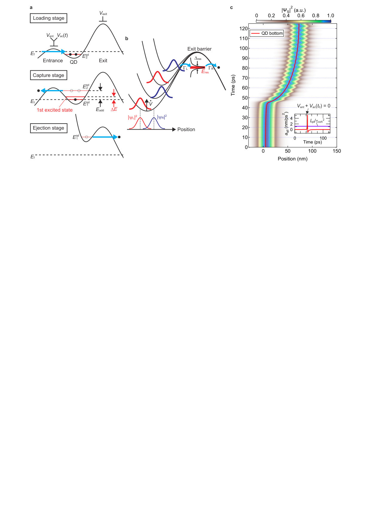 Figure 1
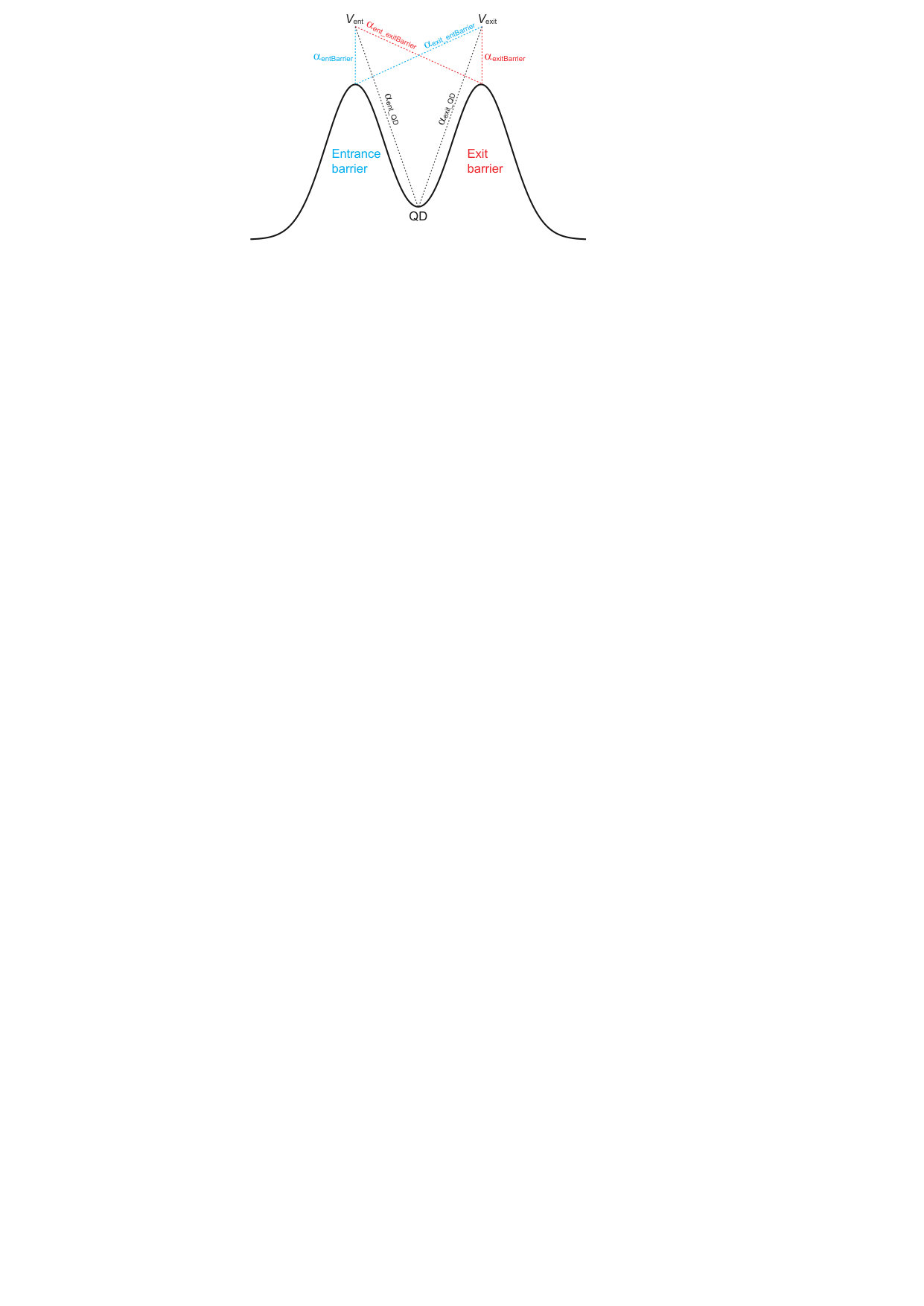 Figure 1
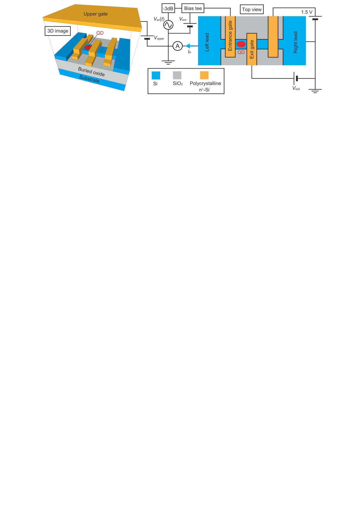 Figure 2
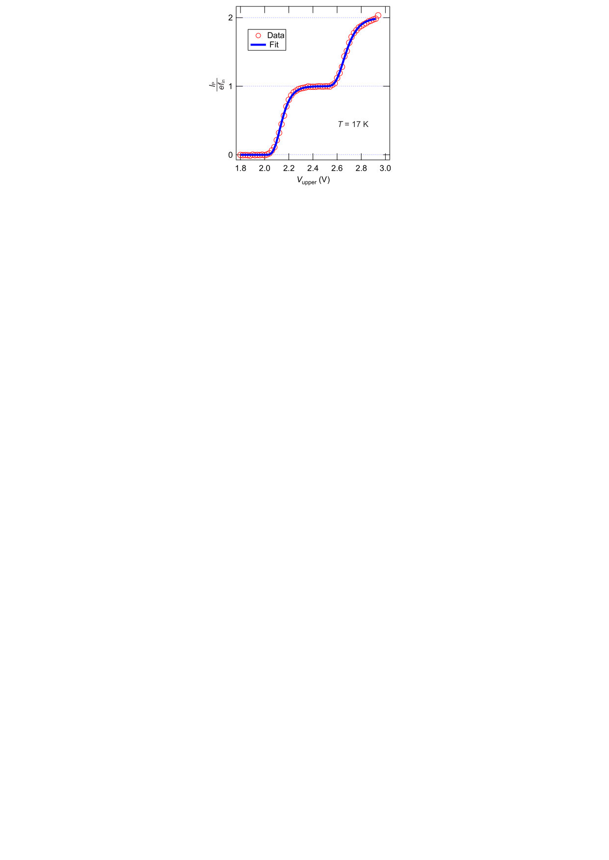 Figure 2
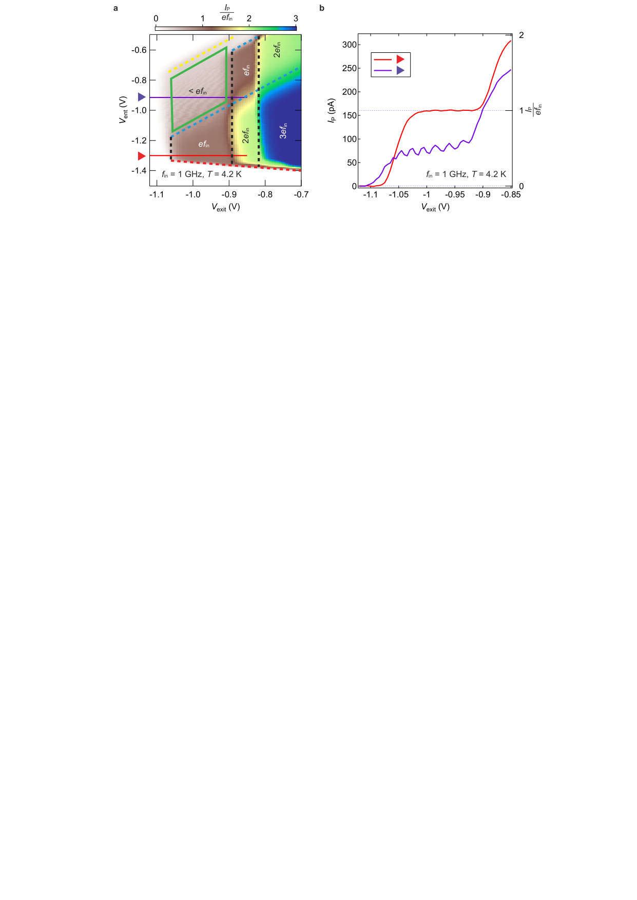 Figure 3
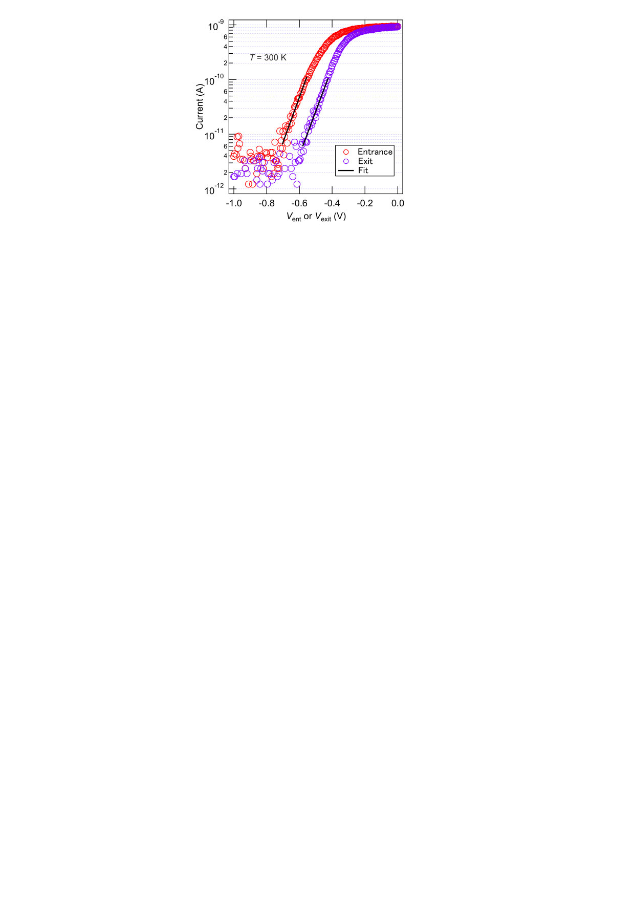 Figure 3
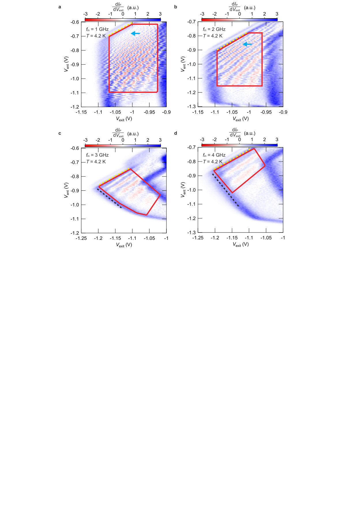 Figure 4
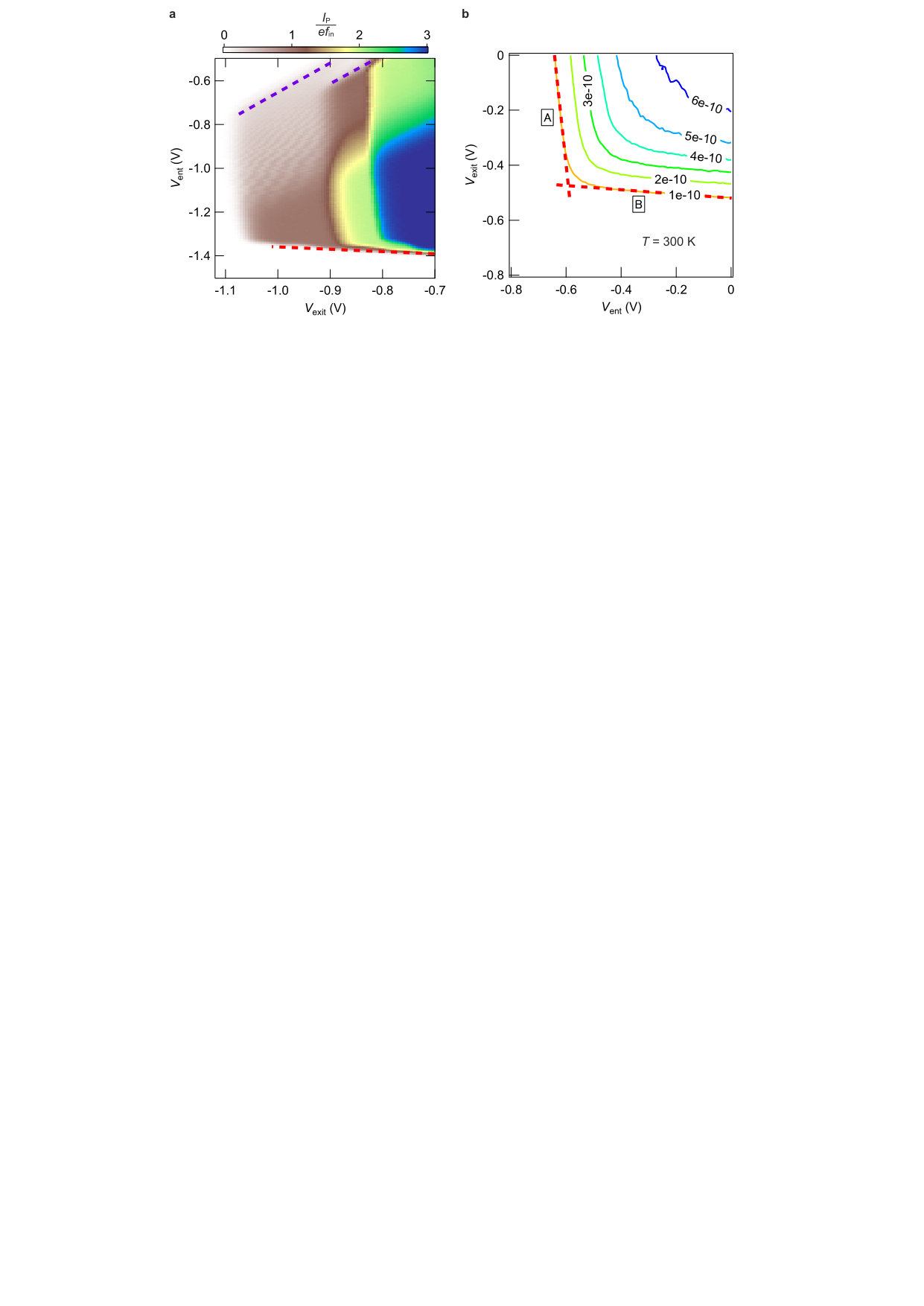 Figure 4
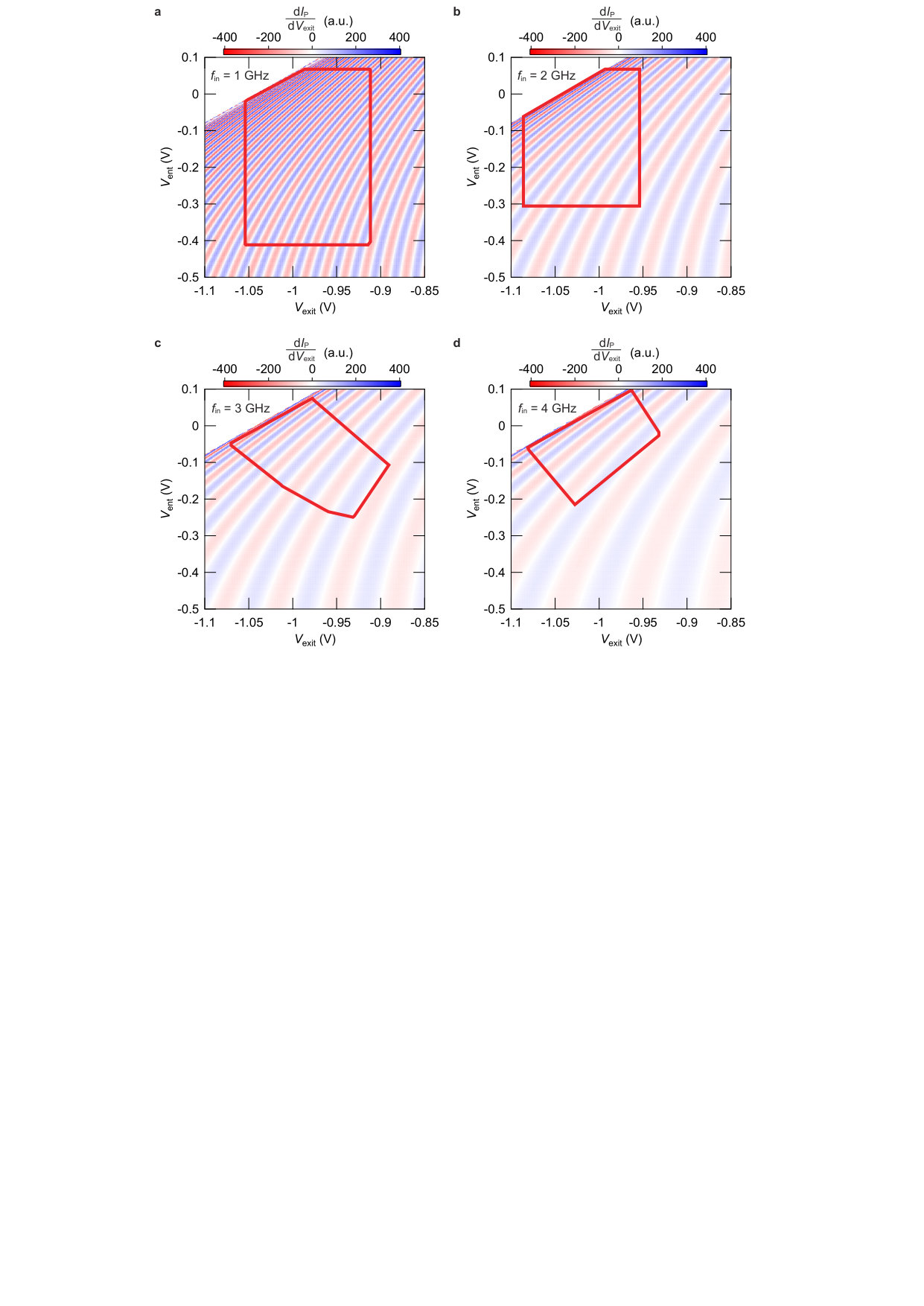 Figure 5
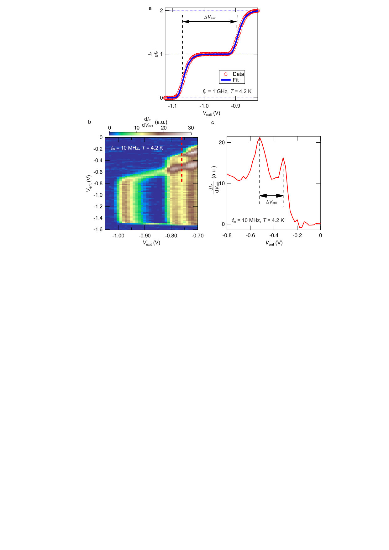 Figure 5
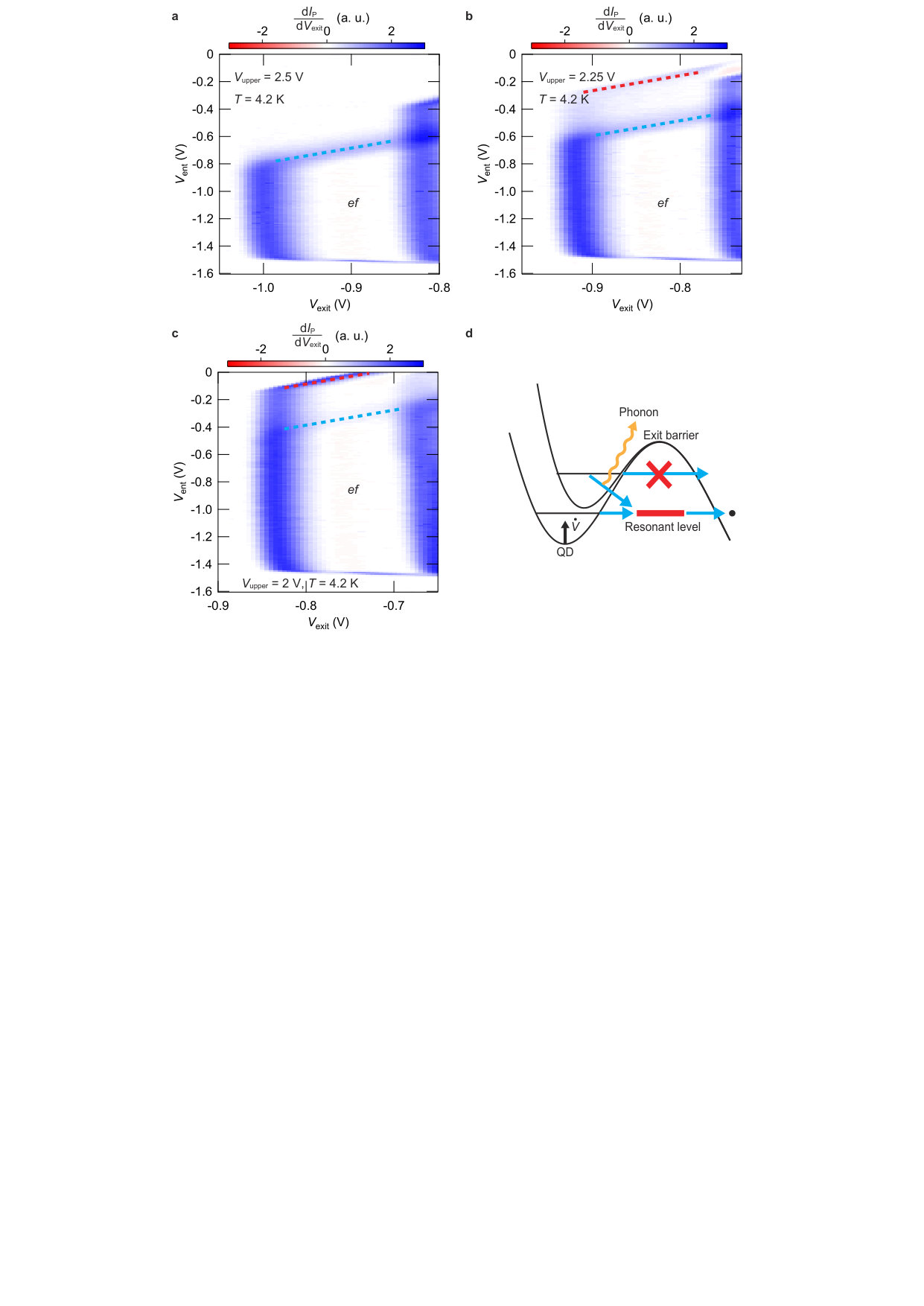 Figure 6
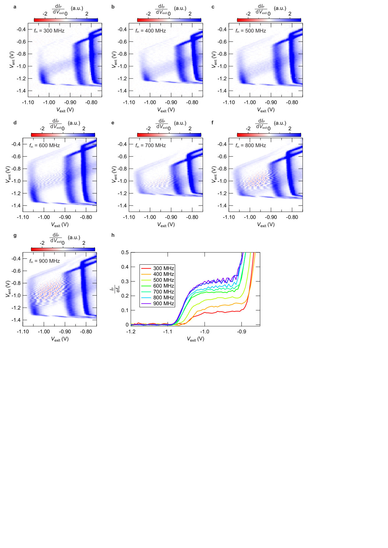 Figure 7
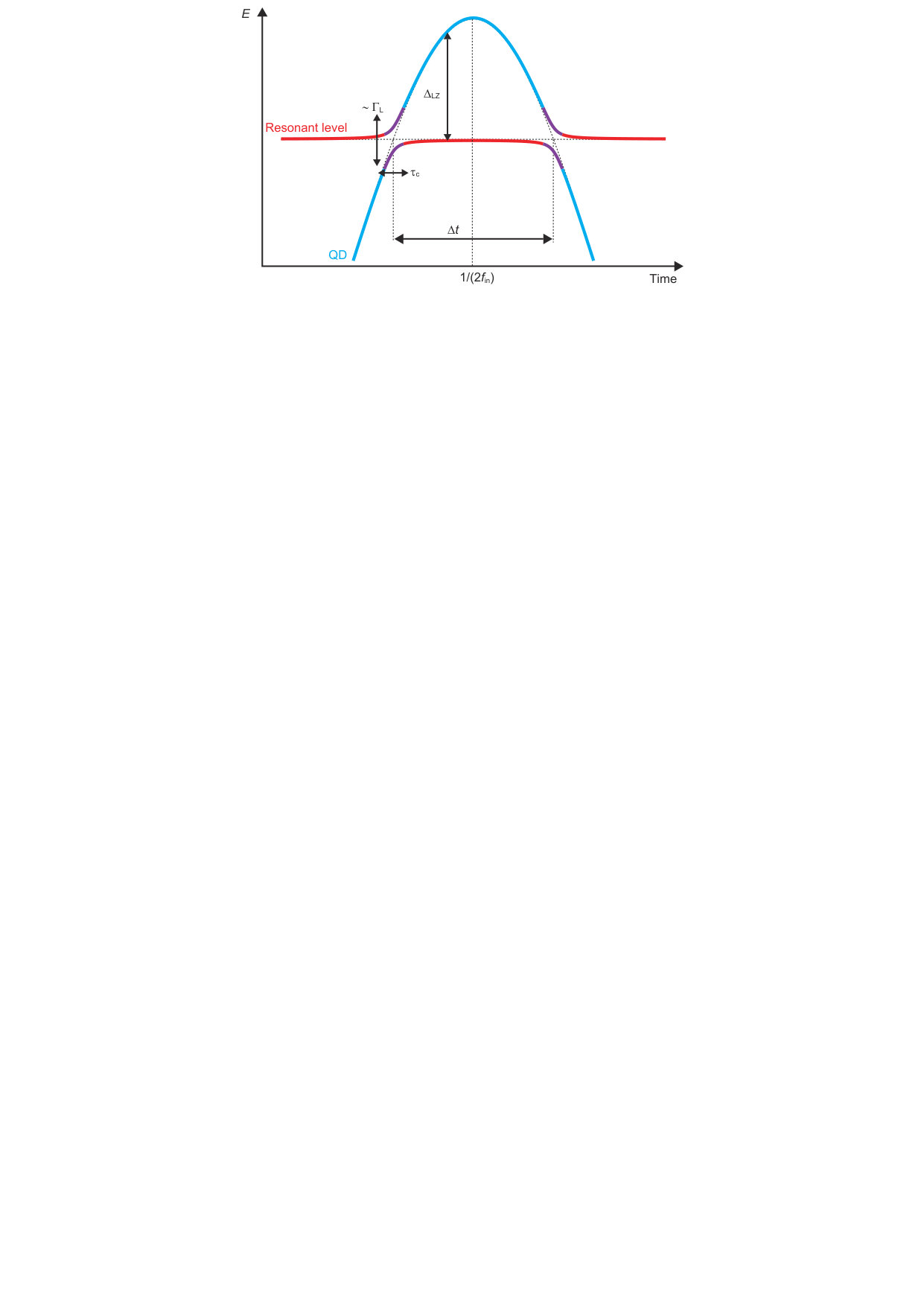 Figure 8
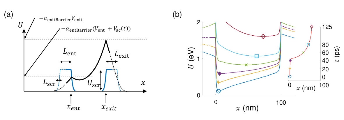 Figure 14
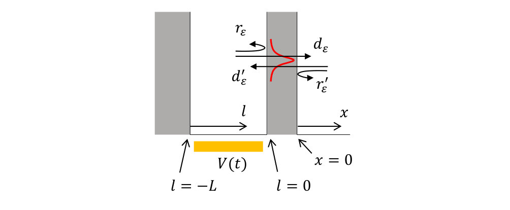 Figure 15
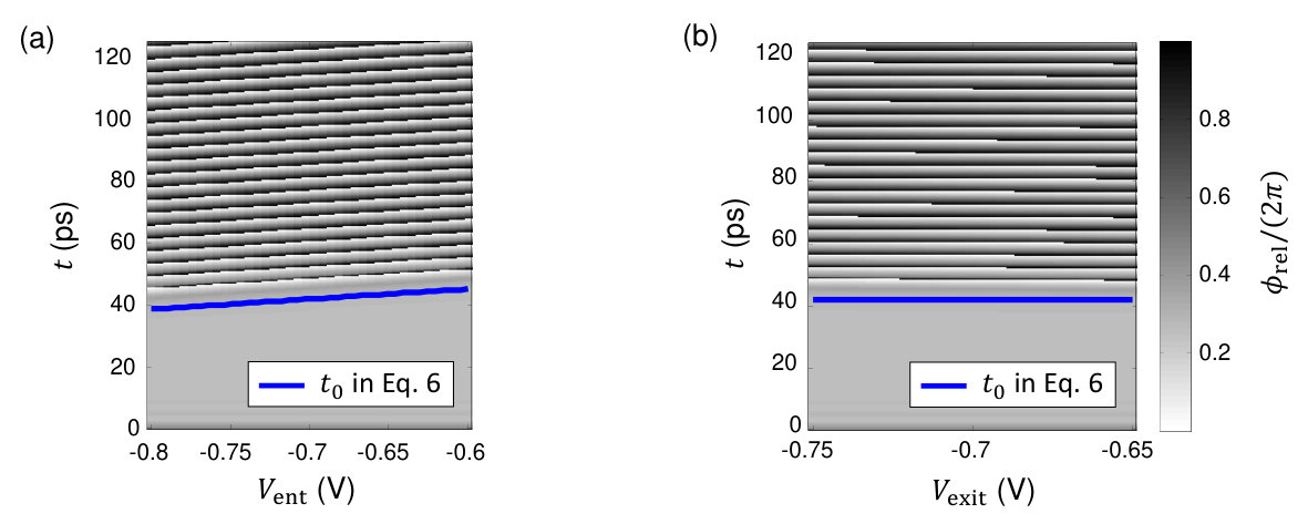 Figure 16
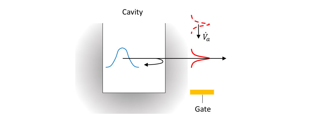 Figure 17
Peer Reviews
No public reviews on file for this paper yet. If you reviewed it on a platform where reviews are public (OpenReview, ICLR, NeurIPS, ICML), you can paste yours below so the community can read it here.
Videos
No videos yet. Explain this paper in a talk, walkthrough, or lecture? Add one.
††thanks: These authors contributed equally to this work.††thanks: These authors contributed equally to this work.
Picosecond coherent electron motion in a silicon single-electron source
Gento Yamahata1)1)1)Electronic mail: [email protected]
NTT Basic Research Laboratories, NTT Corporation, 3-1 Morinosato Wakamiya, Atsugi, Kanagawa 243-0198, Japan
Sungguen Ryu
Department of Physics, Korea Advanced Institute of Science and Technology, Daejeon 34141, Korea
Nathan Johnson
NTT Basic Research Laboratories, NTT Corporation, 3-1 Morinosato Wakamiya, Atsugi, Kanagawa 243-0198, Japan
H.-S. Sim
Department of Physics, Korea Advanced Institute of Science and Technology, Daejeon 34141, Korea
Akira Fujiwara
NTT Basic Research Laboratories, NTT Corporation, 3-1 Morinosato Wakamiya, Atsugi, Kanagawa 243-0198, Japan
Masaya Kataoka
National Physical Laboratory, Hampton Road, Teddington, Middlesex TW11 0LW, United Kingdom
Understanding ultrafast coherent electron dynamics is necessary for application of a single-electron source to metrological standardspekola-rev , quantum information processingSEsouce1 , including electron quantum opticsFeve_opt1 , and quantum sensingNathan_samp ; qsen1 . While the dynamics of an electron emitted from the source has been extensively studiedkataokaSAW ; Feve_sci_coh ; lev-opt ; glat_tomo ; Ubbelohde1 ; Nathan1 , there is as yet no study of the dynamics inside the source. This is because the speed of the internal dynamics is typically higher than 100 GHz, beyond state-of-the-art experimental bandwidthSEsouce1 . Here, we theoretically and experimentally demonstrate that the internal dynamics in a silicon single-electron source comprising a dynamic quantum dot can be detected, utilising a resonant level with which the dynamics is read out as gate-dependent current oscillations. Our experimental observation and simulation with realistic parameters show that an electron wave packet spatially oscillates quantum-coherently at 200 GHz inside the source. Our results will lead to a protocol for detecting such fast dynamics in a cavity and offer a means of engineering electron wave packetsSungguen1 . This could allow high-accuracy current sourcesgib1 ; PTB-ulca1 ; NPL-NTT1 ; Zhao_pump , high-resolution and high-speed electromagnetic-field sensingNathan_samp , and high-fidelity initialisation of flying qubitsyamamoto_fly ; MeunSAW1 .
Owing to recent demonstrations of high-accuracy GHz operationgib1 ; PTB-ulca1 ; NPL-NTT1 ; Zhao_pump , a single-electron pump with a tunable-barrier quantum dot (QD) becomes promising for application to on-demand single-electron sourcespekola-rev . Because of the fast dynamic movement of the QD, there can occur nontrivial electron dynamics, such as non-adiabatic excitationkataoka1 and subsequent coherent time evolution. While the non-adiabatic excitation could degrade the pumping accuracy, a spatial movement of an electron wave packet due to the coherent time evolution can be used for engineering a wave packet emitted from the QDSungguen1 , which could make possible electron quantum optics experiments and high-speed quantum sensing with high resolution. In addition, understanding of the fast electron dynamics could offer insight into quantum computing with QDs. However, the existing standard measurement techniquentte ; Petersson1 ; DKim1 does not have enough bandwidth to detect fast dynamics beyond 100 GHz. In order to overcome the limitation and detect the fast dynamics in the QD, we use a temporal change in a tunnel rate between a resonant level in a tunnel barrier and a QD, which is induced by the dynamic change of the QD potential.
First of all, we explain how coherent oscillations of an electron in a single-electron pump occur. A single-electron pump with a tunable-barrier QD consists of the entrance (Fig. 1a, left) and exit (right) potential barriers, formed by applying gate voltages and , respectivelytunable-barrier1 . An AC voltage with frequency is added to dynamically tune the entrance barrier. The QD energy level is also tuned owing to the cross coupling. When the energy level () of the QD with electrons is lower than the Fermi level , electrons can be loaded from the left lead (loading stage). After that, when is lifted and becomes higher than , the loaded electrons can escape to the left lead. However, when the escape rate is much slower than the barrier-rise rate, the electrons can be dynamically captured by the QD (capture stage)kaestner1 . Finally, the captured electrons can be ejected to the right lead (ejection stage). This gives the pumping current as , where is the elementary charge. Detailed models for these three stages are found in the Supplementary Information.
When is high (typically in the GHz regime), non-adiabatic excitation can occur in the QDkataoka1 . Then, electrons can be in a superposition of the ground state and excited states. In the case that only one electron is captured in the QD, the electron forms a wave packet kataokaSAW ; Sungguen1 moving coherently back and forth between the entrance and exit barriers in the QD, as shown in Fig. 1b. The coherent spatial oscillations can be approximately described by a time-dependent superposition between the instantaneous ground state and the first excited state of the QD,
[TABLE]
where is the probability that the excited state is occupied and is the initial phase. The oscillation period is determined by the energy gap between the ground and first excited states, and it is written as when is approximately time independent. Here, is the Planck constant.
To check the feasibility of the non-adiabatic excitation and coherent dynamics described by Eq. 1, we numerically solve the time-dependent Schrdinger equation with a realistic potential profile (see Supplementary Information). Figure 1c shows a calculated wave-packet distribution as a function of time and position at GHz. The entrance barrier starts to push the QD away from it at around 40 ps, at which the acceleration of the horizontal movement of the QD bottom rapidly increases (inset of Fig. 1c). Around this time, the acceleration is higher than the critical value above which the non-adiabatic excitation occurs, where is the confinement length of the QD and is the electron effective mass. After that there occurs, following Eq. 1, the spatial oscillations at the picosecond scale, which is beyond currently available bandwidth for measurements of coherent charge oscillationsntte ; Petersson1 ; DKim1 .
We propose that such fast coherent oscillations can be detected using a resonant level formed in the exit barrier (Fig. 1b). While the electron moves back and forth, the potential energy of the QD increases from the value at initial time (onset of the non-adiabatic excitation). At time , when the energy becomes aligned with , the electron can be ejected through the exit barrier via the resonant level, generating current. We formulate the ejection probability based on scattering theory (see Supplementary Information) as
[TABLE]
depends on the time difference , which is tuned by changing the gate voltages or the rising speed of the QD bottom. The probability becomes maximal (minimal) when the tuning makes the electron wave packet be located near the exit (entrance) barrier at , resulting in gate-dependent current oscillations. The mean probability depends on the transmission probability through the resonant level and on the ratio of the energy broadening of the resonant level to the energy rise in one period of the spatial oscillations, where is the coupling energy between the resonant level and QD (right lead).
The conditions for observing the gate-dependent current oscillations are
[TABLE]
Under the left inequality, the energy uncertainty of the electron wave packet is smaller than the resonance energy broadening so that the electron can fully pass the resonant levelSungguen1 . The right inequality is also required; in the opposite limit , the current becomes gate-independent because the wave packet reaches the exit barrier many times within the time window where the electron is allowed to pass the resonant level (the limit is also not acceptable because the oscillation amplitude becomes too small, as expected from the expression of ).
To observe the coherent dynamics, we measure a device with a double-layer gate structure on a non-doped silicon wirefrat1 ; NPL-NTT1 at 4.2 K (Fig. 2). The fabrication process and measurement detail are described in Methods. This kind of device often has a resonant level in the exit barrier, which most likely originates from an interface trap leveltrap1 ; trap2 ; rossi_trap . Such a resonant level can be identified by investigating a map of as a function of and (Fig. 3a). In the map, there are several threshold voltages indicated by dashed lines. Along the red solid line, we observe an current plateau (Fig. 3b). The signature of the resonant level appears in a wide region with a current less than indicated by the green parallelogram, where the direct tunneling through the exit barrier is suppressed and the resonant and inelastic tunnelingFujiPh via the resonant level can be resolved.
We observe current oscillations in the region with the resonant-level signature (see the line cut in Fig. 3b). In this region, the current (normalised by ) through the resonant level increases with increasing , indicating the non-adiabatic excitation (the detail is discussed in the Supplementary Information). To examine the current oscillations, we plot as a function of and at 1 to 4 GHz (Fig. 4). The period of the current oscillations increases with increasing . This is expected from Eq. 2 because increases with increasing . In addition, the period becomes shorter when the trap-ejection line (the yellow dashed line) approaches and the oscillation lines slightly bend towards the bottom right.
The above features agree with the coherent spatial oscillations described by Eqs. 1 and 2. To see this, we simplify Eq. 2 as
[TABLE]
which focuses on the position of the current oscillations; the simplification is valid when , 0.5, and . The final time , at which the energy of the electron becomes aligned with , is given by (see Supplementary Information),
[TABLE]
where and are voltage-to-energy conversion factors related to the entrance and exit gate, respectively. The initial time is chosen to be the onset of the non-adiabatic excitation, at which the entrance gate voltage becomes negative so that the entrance barrier starts to push the QD away from it. The onset is determined by (see also the inset of Fig. 1c), equivalently
[TABLE]
By estimating and from the measurement results (see Supplementary Information), we simulate the gate dependence of the current oscillations. Figure 5 shows calculated current-oscillation maps as a function of and at 1 to 4 GHz, corresponding directly to Fig. 4. The peak positions with respect to the trap-ejection line are well reproduced, including the shorter period at the trap-ejection line and the curvature of the oscillation lines (see also discussion in the Supplementary Information).
Importantly, the only fit parameter of the calculation is meV. The QD size () estimated from is about 40 nm, which is reasonable with respect to the lithographic size of our device (the first electron can be confined at the QD bottom)nttg1 . The fact that the current oscillations are reproduced using only reasonable parameters supports that the experimental observation is related to the coherent dynamics of the wave packet. We highlight that meV corresponds to ps ( GHz), which is far in excess of currently achievable bandwidthSEsouce1 ; ntte ; Petersson1 ; DKim1 .
Here, we roughly evaluate Eq. 3 using the above results to investigate the validity of the experimental observation (see Supplementary Information), and find that 1 meV meV for meV and GHz. The range of is acceptable, in comparison with the energy difference ( 10 meV, estimated from the result in Fig. 3a) between the top of the exit barrier and the resonant level; the energy difference should be larger than to observe the current oscillations.
We note that we have considered other possible mechanisms for observed current oscillations, but have not found any alternative explanations. We can neglect the possibilities of the phonon density of statesPhonon_DQD and the Fabry-Perot interference through an unintentionally-formed QDFabryPerot1 because they should be independent of . We also rule out Landau-Zener-Stckelberg interferenceLZSSi1 (see Supplementary Information).
Our results imply a protocol for measuring such a fast dynamics. We suggest that when any kind of dynamic control of a particle in a cavity, including its initialisation, excitation, and coherent oscillations, is repeated by frequency , the coherent dynamics can be detected as oscillations of the current of the particle through the resonant level, by coupling the cavity to any kind of a resonant level driven by an AC signal with (see Supplementary Information).
Finally, we stress that the understanding of the internal coherent dynamics is useful for engineering an emitted wave packet, for example, to be a Gaussian formSungguen1 . A Gaussian wave packet has a narrow wave-packet width in terms of energy or time (achieving the Heisenberg uncertainty limit), and such a narrow wave packet could lead to ultimately high-speed and high-resolution quantum sensingNathan_samp and enhancement of the visibility of electron quantum optics experimentsFeve_opt1 . Furthermore, since internal coherent dynamics affect the initialisation of flying qubitsyamamoto_fly ; MeunSAW1 , this understanding could contribute to the improvement of the initialisation fidelity. In addition, further investigation of the non-adiabatic excitation using the method proposed in this Letter could lead to improvement of the accuracy of single-electron pumping, which contributes to the realisation of high-accuracy current sources.
Acknowledgements
We thank K. Chida, H. Tanaka, T. Karasawa, S. P. Giblin, J. D. Fletcher, and T. J. B. M. Janssen for useful discussions. This work was partly supported by JSPS KAKENHI Grant Number JP18H05258 and by the UK Department for Business, Innovation, and Skills and by the EMPIR 15SIB08 e-SI-Amp Project. The latter project has received funding from the EMPIR programme co-financed by the Participating States and from the European Union’s Horizon 2020 research and innovation programme. This work was also supported by the National Research Foundation (Korea NRF) funded by Korea Government via the SRC Center for Quantum Coherence in Condensed Matter (Grant Number 2016R1A5A1008184).
Author contributions
G.Y. measured the device, analyzed the data, and performed the calculation of the pump map. S.R. performed the numerical calculation of the Schrdinger equation. G.Y. and M.K. conceived the idea of the experiment. S.R. and H.S. developed the theory of the coherent dynamics. N.J. took supporting data of the current oscillations. A.F. fabricated the device. All authors discussed the results. G.Y., S.R., and H.S. wrote the manuscript with feedback from all authors. M.K., A.F., and H.S. supervised the project.
Competing interests
The authors declare no competing interests.
Additional information
Supplementary information is available for this paper.
Methods
Device fabrication
A silicon wire is patterned using electron beam lithography and dry etching on a non-doped silicon-on-insulator wafer with a buried-oxide thickness of 400 nm. After formation of thermally grown silicon dioxide with a thickness of 30 nm, three lower gates made of heavily-doped polycrystalline silicon are formed using chemical vapor deposition, electron beam lithography, and dry etching. The spacing of the adjacent lower gates is 100 nm. Then, an inter-layer silicon dioxide is deposited using chemical vapor deposition. Next, an upper gate made of heavily-doped polycrystalline silicon is formed using chemical vapor deposition, optical lithography, and dry etching. Then, the left and right leads are heavily doped using ion implantation, during which the upper gate is used as an implantation mask. Finally, aluminum pads are formed to obtain an Ohmic contact. The width and thickness of the silicon wire are 15 and 10 nm, respectively.
Measurement detail
Measurements were performed in liquid He at 4.2 K. DC and AC voltages were applied using the Keithley 213 voltage source and Keysight 83623B signal generator, respectively. The pumping current was measured using the Keithley 6514 electrometer. DC voltage is applied to the upper gate to induce electrons in the silicon wire. and are applied to the entrance and exit gates, respectively, where with amplitude .
The reference list from the paper itself. Each links out to its DOI / PubMed record.
- 1(1) Pekola, J. P. et al. Single-electron current sources: Toward a refined definition of the ampere. Rev. Mod. Phys. 85 , 1421 (2013).
- 2(2) Bäuerle, C. et al. Coherent control of single electrons: a review of current progress. Rep. Prog. Phys. 81 , 056503 (2018).
- 3(3) Bocquillon, E. et al. Electron quantum optics: Partitioning electron one by one. Phys. Rev. Lett. 108 , 196803 (2012).
- 4(4) Johnson, N. et al. Ultrafast voltage sampling using single-electron wavepackets. Appl. Phys. Lett. 110 , 102105 (2017).
- 5(5) Degen, C. L., Reinhard, F. & Cappellaro, P. Quantum sensing. Rev. Mod. Phys. 89 , 035002 (2017).
- 6(6) Kataoka, M. et al. Coherent time evolution of a single-electron wave function. Phys. Rev. Lett. 102 , 156801 (2009).
- 7(7) Bocquillon, E. et al. Coherence and indistinguishability of single electrons emitted by independent sources. Science 339 , 1054–1057 (2013).
- 8(8) Dubois, J. et al. Minimal-excitation states for electron quantum optics using levitons. Nature 502 , 659–663 (2013).