Charge detection in gate-defined bilayer graphene quantum dots
A. Kurzmann, H. Overweg, M. Eich, A. Pally, P. Rickhaus, R. Pisoni, Y., Lee, K. Watanabe, T. Taniguchi, T. Ihn, and K. Ensslin

TL;DR
This paper demonstrates charge detection in bilayer graphene quantum dots using an integrated, high-quality charge detector without etching, capable of sensing individual electron charging events and coupled quantum dot states.
Contribution
It introduces a novel, etching-free fabrication method for bilayer graphene quantum dots with integrated charge detection, enabling sensitive measurement of single-electron charging.
Findings
Charge detector detects single-electron charging events.
Potential change causes up to 77% current step in detector.
Detection of charging states in coupled quantum dots.
Abstract
We report on charge detection in electrostatically-defined quantum dot devices in bilayer graphene using an integrated charge detector. The device is fabricated without any etching and features a graphite back gate, leading to high quality quantum dots. The charge detector is based on a second quantum dot separated from the first dot by depletion underneath a 150 nm wide gate. We show that Coulomb resonances in the sensing dot are sensitive to individual charging events on the nearby quantum dot. The potential change due to single electron charging causes a step-like change (up to 77 %) in the current through the charge detector. Furthermore, the charging states of a quantum dot with tunable tunneling barriers and of coupled quantum dots can be detected.
Click any figure to enlarge with its caption.
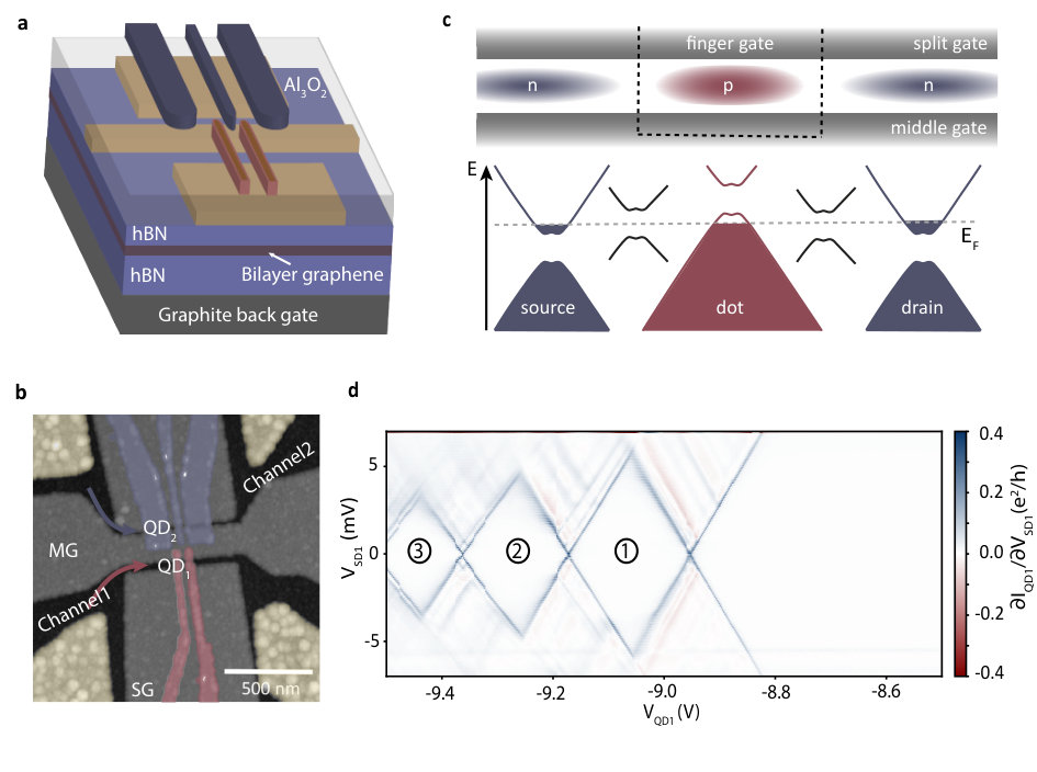 Figure 1
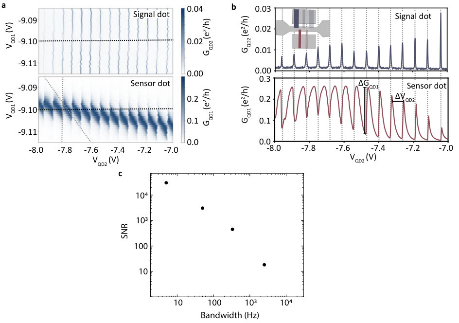 Figure 2
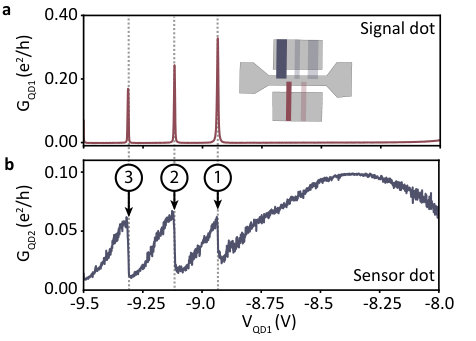 Figure 3
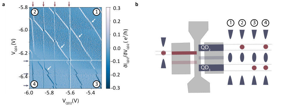 Figure 4
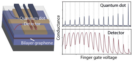 Figure 5
| Publication | Fabrication | Detector | |
|---|---|---|---|
| Güttinger et al. (2008) 28 | Etched | Resonance in a nanoribbon | |
| Wang et al. (2010) 29 | Etched | SET | |
| Fringes et al. (2011) 30 | 0.005 | Etched | Resonance in a nanoribbon |
| Güttinger et al. (2011) 33 | 0.05 | Etched | Resonance in a nanoribbon |
| Volk et al. (2013) 31 | 0.002 | Etched | Resonance in a nanoribbon |
| This work (2019) | 0.2 | Gate-defined | Quantum dot resonance |
Peer Reviews
No public reviews on file for this paper yet. If you reviewed it on a platform where reviews are public (OpenReview, ICLR, NeurIPS, ICML), you can paste yours below so the community can read it here.
Videos
No videos yet. Explain this paper in a talk, walkthrough, or lecture? Add one.
Charge Detection in Gate-Defined Bilayer Graphene Quantum Dots
Annika Kurzmann
Hiske Overweg
Marius Eich
Alessia Pally
Peter Rickhaus
Riccardo Pisoni
Yongjin Lee
Solid State Physics Laboratory, ETH Zürich, CH-8093 Zürich, Switzerland
Kenji Watanabe
Takachi Taniguchi
National Institute for Material Science, 1-1 Namiki, Tsukuba 305-0044, Japan
Thomas Ihn
Klaus Ensslin
Solid State Physics Laboratory, ETH Zürich, CH-8093 Zürich, Switzerland
Abstract
We report on charge detection in electrostatically-defined quantum dot devices in bilayer graphene using an integrated charge detector. The device is fabricated without any etching and features a graphite back gate, leading to high quality quantum dots. The charge detector is based on a second quantum dot separated from the first dot by depletion underneath a 150 nm wide gate. We show that Coulomb resonances in the sensing dot are sensitive to individual charging events on the nearby quantum dot. The potential change due to single electron charging causes a step-like change (up to 77%) in the current through the charge detector. Furthermore, the charging states of a quantum dot with tunable tunneling barriers and of coupled quantum dots can be detected.
keywords:
Bilayer graphene, quantum dot, charge detection, tunneling, multidots
1 Introduction
Graphene is a promising candidate for future nano-electronic devices including building blocks for quantum information processing. Reasons are the expected long spin lifetimes 1 and high carrier mobilities 2, 3, 4. Experimentally these spin lifetimes have not been demonstrated yet. For progress in this direction 5 a device is needed that allows to confine charges and simultaneously measure their dynamics in a time-resolved way. This is possible with a charge detector in close proximity to a graphene quantum dot (QD). In GaAs based devices a combination of QDs and QPCs allowed to detect spin-qubit states 5, 6 and molecular states in coupled QDs 7. Furthermore, charge detection can be used to investigate tunneling dynamics of charges in a time-resolved way 8, 9 and to obtain the full counting statistics of the charge current and the charge occupation.
Recent experiments show the fabrication and measurement of quantum dots 10, 11, 12 and quantum point contacts 13, 11, 14 in bilayer graphene, that are comparable to GaAs devices. Bilayer graphene offers the possibility to electrostatically define nanostructures by opening a band gap through the application of a displacement field normal to the bilayer plane 15, 16, 17. With a suitable design of top and back gate electrodes, it allows for electrostatic confinement of charge carriers in high quality bilayer graphene devices. These devices use encapsulation in hexagonal boron nitride (hBN) 18, edge contacts 19 and a graphite back gate 10, 11, 12, that screens charge impurities trapped in the silicon oxide substrate 20.
In previous experiments, exfoliated graphene flakes have been etched to fabricate graphene nanoribbons 21, 22, 23, single-electron-transistors (SETs) 24 and quantum dots 25, 26 with charge detector 27, 28, 29, 30, 31. A disadvantage of this fabrication method are charge carrier localizations at the rough sample edges, that can lead to transmission resonances from the tunneling barriers which may dominate the entire device behavior in certain parameter regimes. 32.
Here, we use bilayer graphene with its electrostatically induced band gap to fabricate a fully gate-defined device with quantum dots, that are also used as charge detectors. The quality of the bilayer graphene quantum dots and the amplitude of the detection signal matches that of the traditional semiconductors Si and GaAs. A comparison of the charge detection signal in different etched devices with our electrostatically defined device is shown in Table 1. We measure a detection signal that exceeds the best previous results by more than a factor of two. Furthermore, a tunable gate-defined quantum dot is used as charge detector instead of a random resonance in a nano ribbon. The quality of our device and the good control of the charge detector makes it interesting for future investigations of the spin and valley coherence and relaxation rates.
2 Characterization
The van-der-Waals heterostructure has been fabricated using the dry transfer method 18. A schematic of the stack is shown in Figure 1a. It consists (from bottom to top) of a graphite back gate (grey), a bottom hexagonal boron nitride (hBN) flake (33 nm thick, light blue in Figure 1a), the bilayer graphene flake (dark red) and a top hBN flake (35 nm thick, light blue). The bilayer graphene flake is electrically contacted using edge contacts 19 and metal deposition (Cr/Au). In a next step the Cr/Au (5 nm/20 nm for the small structures and 10 nm/60 nm for the connections to the bond pads) split gates and middle gate (SG and MG, grey in Figure 1b) are deposited on top of the stack. The middle gate is 150 nm wide and separated from the split gates by 100 nm on both sides, forming two channels (black in Figure 1b). An insulating 30 nm thick layer separates the split gates and the Cr/Au (thickness similar to SGs) finger gates (blue and red in Figure 1b). The wider finger gates have a width of 120 nm, the narrow one is 20 nm wide. Their lateral separation is 90 nm. A quantum dot can be formed below each of the finger gates (two quantum dots in channel 1 and three dots in channel 2). The atomic force microscope image in Figure 1b shows the lateral layout of the two top gate layers with split gates (gray), middle gate (gray), finger gates (blue and red) and the Ohmic contacts (yellow).
The graphite back gate and the split gates can be used to (i) open a band gap below the gates, and (ii) tune the Fermi energy into the band gap, which renders these regions insulating. N-type channels with a lithographic width of are formed between the gates (see Figure 1c blue n-doped regions) by applying a positive voltage to the graphite back gate () and a negative voltage to the split gates (). The MG is used to separate the channels, where a gate width of is needed to avoid leakage currents between them. Separate source-drain bias voltages are applied to each channel using pairs of ohmic contacts (Figure 1b).
Using one of the finger gates the Fermi-energy in the bilayer graphene region below the finger gate can be tuned into the band gap (pinch-off) or into the p-region (Figure 1c red), where a QD confining holes is formed. The band structure is sketched in Figure 1c (lower panel) with source and drain contacts in the n-regions and the hole QD below the finger gate. Between the n- and p-regions the Fermi-energy (at the edges of the finger gate, see Figure 1c) lies in the band gap, hence natural tunnel barriers for the quantum dot are formed 12. Each quantum dot with its sharp Coulomb resonances is also a sensitive detector for single charges in any other QD nearby. The resonances of the QDs are even more sensitive than a QPC, due to the steeper slope of the conductance versus finger gate voltage.
All measurements presented here were performed in a dilution refrigerator with an electronic base temperature of 60 mK in a two-terminal DC setup with a bias voltage applied between source and drain, and the drain contact grounded. The integration time for current measurements was set to 20 ms.
Figure 1d shows a measurement of Coulomb blockade diamonds of QD1 formed underneath the left red-colored finger gate in channel 1 (see Figure 1b). We measure the differential current in channel 1 as a function of the finger gate voltage forming QD1 and the DC source-drain bias . In the Coulomb blockade diamonds we see single holes charging into the quantum dot at for . From the Coulomb blockade diamonds a charging energy of about and a finger gate lever arm can be determined.
3 Results and discussion
For the charge detection experiment shown in Figure 2, QD1 in channel 1 is used as sensing dot. A source-drain bias of (optimized for the detection signal) is applied across the sensing dot and the finger gate voltage is chosen so that sequential tunneling through QD1 is possible and a current is measured. At this finger gate voltage the quantum dot is a sensitive detector for changes of the charge configuration in its environment. A small change in the electrostatic environment of the dot leads to a shift of the Coulomb resonance in energy (or equivalently, in finger gate voltage ) and therefore to a change in the conductance through channel 1.
A second p-type quantum dot (signal dot QD2) is formed below the left blue gate in channel 2 (Figure 1a), by tuning the finger gate voltage . The linear conductance through channel 2 is shown in Figure 2a upper panel, where the gate voltages and are changed and a source-drain voltage of across the signal dot is applied. By changing we scan across one Coulomb resonance of QD1 (detector dot) and measure the conductance in channel 1 and channel 2 at the same time. The upper panel in Figure 2a shows regularly spaced Coulomb resonances in the conductance of the signal dot, which slightly shift by changing .
These resonances are observed through charge detection in the lower panel of Figure 2a. A line-cut in direction shows a Coulomb resonance of the sensing dot (QD1), that shifts to more negative , when is increased. The diagonal shift of the sensing dots resonance (marked by diagonal dashed line) is due to the cross capacitance between the sensing dot and the finger gate voltage defining the signal dot. From this shift a ratio between the lever arm of the blue gate () on the sensor dot and the red gate () on the sensor dot \alpha_{V_{\text{QD2}}-\text{QD1}}/\alpha_{\text{V_{\text{QD1}}-QD1}}=0.07 is calculated.
We identify single charging events in the signal dot as abrupt shifts of the conductance resonance in the sensing dot (marked with vertical dashed line), aligned with the Coulomb resonances of the signal dot (see vertical dashed lines). Line cuts from Figure 2a at are shown in Figure 2b. Regularly spaced conductance resonances are observed in Figure 2b (upper panel), when sequential tunneling through the signal dot is possible.
The corresponding conductance measured simultaneously in the detector channel is shown in the lower panel in Figure 2b. We observe a broadened resonance with its maximum at and a width of with step-like features on top. The resonance is broader in than in , due to the much smaller lever arm of the blue finger gate on the sensing dot as compared to the red finger gate. The conductance steps (marked with vertical dashed lines) are related to a shift in the resonance of the sensing dot with respect to the signal dot’s voltage .
From an analysis of the charging events an average shift in (see Figure 2b) is observed. The conductance in the detector channel (see Figure 2b) changes by up to 77% for a single charging event. This change in conductance is compared to other devices in Graphene in Table 1. Furthermore, we evaluate the signal to noise ratio (SNR) of at a measurement bandwidth of 50 Hz. is the variance of the detector current and the current change in the detector due to one charging event. In Figure 2c the SNR of the charge detection signal is shown for different measurement bandwidth. From these measurements we expect a maximal bandwidth of 10 kHz for our measurement, which is higher than in etched graphene devices 33. The tunneling rates in the presented device are higher than the maximal measurement bandwidth, so that time-resolved measurements of electron tunneling is not possible in this device.
In the following, we exchange the role of the two dots, to confirm that we are able to fully deplete the quantum dot and fill it with individual holes. The quantum dot in channel 2 (QD2) will be used as the sensing dot. The conductances through the signal dot in channel 1 (QD1) is shown in Figure 3a. For QD1, we can clearly see a first Coulomb resonance (marked by ①) in the conductance of the channel 1 at . The conductances and of both channels are shown in Figure 3a and b, while the gate voltage of the signal dot (QD1) is changed and a source-drain bias of is applied to both channels. In the conductance of the detector a first step is also observed at about .
Furthermore, QDs with tunable tunneling barriers and multiple-dots can be formed in channel 2 using the two broader finger gates (blue in Figure 4b).12 Figure 4a shows the differential conductance of the charge detector (the conductance change through the signal dot is lower than our measurement resolution) as function of the gate voltages and that were applied to the two outer finger gates in channel 2. Three distinct sets of resonances are observed vertical (marked with red arrows), horizontal (marked with blue arrows) and diagonal (marked with white arrows) resonances in Figure 4a). The measurement can be divided into four quadrants (① to ④), separated by the white dashed lines. The corresponding sketch of the charge carrier distributions along channel 2 is shown in Figure 4b. In the first quadrant of Figure 4a we observe diagonal resonances only, that belong to a single electron dot formed between the two outer gates in channel 2 (dark blue in Figure 1a and Figure 4b). The two finger gates are tuned close to the charge neutrality point, thus creating tunneling barriers between the source and drain contacts (see Figure 4b ①). Both gates have the same lever arm on the resonances of this dot, leading to diagonal resonances with a slope of about -1 in this measurement. The tunneling barriers of this dot are tunable, which allows for changing the tunneling rates through the dot.
By decreasing the voltages of the finger gates and further, we can form double- and triple-dots in channel 2 (sketches of the charge carrier density in the channel are shown in Figure 4b ② to ④) similar as demonstrated in Ref. 12. Charge occupation of these multidots, is also detected using QD1 as the charge detector. On the one hand, the gate voltage on the left outer finger gate in channel 2 is more negative and a hole dot forms below the gate. Hence, additional vertical resonances (marked with red arrows) are observed in region ② at and (see schematic picture ② in Figure 4b). For this situation of an electron-hole double-dot, we observe the typical honeycomb pattern using the charge detector.
On the other hand, we decrease the voltage on finger gate 3 () such that a hole QD is formed below this gate. We observe horizontal resonances in region ③ in Figure 4a ( and , marked with blue arrows), which are not influenced by . In region ④ in Figure 4a, three dots are formed- one p-type QD below each of the gates and an n-type dot between them. This leads to diagonal resonances for the tunneling through the electron dot in the middle, horizontal resonances for tunneling through QD3 and vertical line for tunneling through QD2.
The three dots measured in Figure 4a have different distances to the charge detector. Hence, charging the different dots leads to different energy shifts of the sensing dots resonance. The distance between the signal dot and the sensing dot changes from (dot between the gates, blue in Figure 4b) to (dot below left gate in Figure 4b). The energy shift of the detector resonance is evaluated from the detection signal using the shift in gate voltage and the relative lever arms , and . It decreases with the distance between sensing and signal dot from to in agreement with a Coulomb screening model. Our sample design allows for a minimal distance of between the sensing dot and the signal dot, which leads to an energy shift of which is of the same order as the charging energy of the sensing dot.
In conclusion, we presented an electrostatically-defined device that allows us to detect single charge carriers in bilayer graphene quantum dots. Using conductance resonances in the Coulomb-blockade regime of a second quantum dot as a sensitive detector, we reached a maximum relative conductance change of 77% for charge detection. Our measurements show that a width of for the MG is sufficient to avoid leakage between the sensing and signal dot and to reach a high signal-to-noise ratio in the detector. Using this device, we were able to show complete depletion of one of the quantum dots. Furthermore, we were able to observe the changes in the charge state of a quantum dot with tunable tunneling barriers, and of a multi-dot system. In the multi-dot regime, the charge detection enables us to determine the number of charge carriers in each of the dots. Our experiments demonstrate a device that is needed as the starting point for time-resolved measurements in graphene quantum dots, which may allow us to investigate the spin-lifetime in graphene 5.
4 Acknowledgments
We thank Peter Märki, Erwin Studer, as well as the FIRST staff for their technical support. We also acknowledge financial support from the European Graphene Flagship, the Swiss National Science Foundation via NCCR Quantum Science and Technology, the EU Spin-Nano RTN network and ETH Zurich via the ETH fellowship program. Growth of hexagonal boron nitride crystals was supported by the Elemental Strategy Initiative conducted by the MEXT, Japan and the CREST (JPMJCR15F3), JST.
The reference list from the paper itself. Each links out to its DOI / PubMed record.
- 1Trauzettel et al. 2007 Trauzettel, B.; Bulaev, D. V.; Loss, D.; Burkard, G. Spin qubits in graphene quantum dots. Nature Physics 2007 , 3 , 192
- 2Novoselov et al. 2005 Novoselov, K. S.; Geim, A. K.; Morozov, S.; Jiang, D.; Katsnelson, M.; Grigorieva, I.; Dubonos, S.; Firsov, A. Two-dimensional gas of massless Dirac fermions in graphene. Nature 2005 , 438 , 197
- 3Zhang et al. 2005 Zhang, Y.; Tan, Y.-W.; Stormer, H. L.; Kim, P. Experimental observation of the quantum Hall effect and Berry’s phase in graphene. Nature 2005 , 438 , 201
- 4Banszerus et al. 2015 Banszerus, L.; Schmitz, M.; Engels, S.; Dauber, J.; Oellers, M.; Haupt, F.; Watanabe, K.; Taniguchi, T.; Beschoten, B.; Stampfer, C. Ultrahigh-mobility graphene devices from chemical vapor deposition on reusable copper. Science advances 2015 , 1 , e 1500222
- 5Elzerman et al. 2004 Elzerman, J.; Hanson, R.; Van Beveren, L. W.; Witkamp, B.; Vandersypen, L.; Kouwenhoven, L. P. Single-shot read-out of an individual electron spin in a quantum dot. Nature 2004 , 430 , 431
- 6Petta et al. 2005 Petta, J. R.; Johnson, A. C.; Taylor, J. M.; Laird, E. A.; Yacoby, A.; Lukin, M. D.; Marcus, C. M.; Hanson, M. P.; Gossard, A. C. Coherent manipulation of coupled electron spins in semiconductor quantum dots. Science 2005 , 309 , 2180–2184
- 7Di Carlo et al. 2004 Di Carlo, L.; Lynch, H.; Johnson, A.; Childress, L.; Crockett, K.; Marcus, C.; Hanson, M.; Gossard, A. Differential charge sensing and charge delocalization in a tunable double quantum dot. Physical review letters 2004 , 92 , 226801
- 8Gustavsson et al. 2006 Gustavsson, S.; Leturcq, R.; Simovič, B.; Schleser, R.; Ihn, T.; Studerus, P.; Ensslin, K.; Driscoll, D.; Gossard, A. Counting statistics of single electron transport in a quantum dot. Physical review letters 2006 , 96 , 076605