Exciton routing in the heterostructure of TMD and paraelectrics
V. Shahnazaryan, O. Kyriienko, H. Rostami

TL;DR
This paper introduces a method to control and route excitons in TMD monolayers by exploiting the temperature-sensitive dielectric properties of a paraelectric substrate, enabling spatial energy modulation and exciton flow.
Contribution
It presents a novel approach for exciton routing using substrate dielectric permittivity changes induced by temperature variations in TMD heterostructures.
Findings
Substrate temperature significantly affects TMD exciton properties.
Localized heating creates exciton energy gradients and directs exciton flow.
Large dielectric screening in SrTiO₃ enhances exciton energy modulation.
Abstract
We propose a scheme for the spatial exciton energy control and exciton routing in a transition metal dichalcogenide (TMD) monolayer which lies on a quantum paraelectric substrate. It relies on the ultrasensitive response of the substrate dielectric permittivity to temperature changes, allowing for spatially inhomogeneous screening of Coulomb interaction in a monolayer. As an example, we consider the heterostructure of TMD and strontium titanate oxide SrTiO, where large dielectric screening can be attained. We study the impact of substrate temperature on the characteristic electronic features of TMD monolayers such as the particle bandgap and exciton binding energy, Bohr radius and nonlinearity (an exciton-exciton interaction). The combination of particle bandgap and exciton binding energy modulation results in the shift of the exciton resonance energy. Applying local heating, we…
Click any figure to enlarge with its caption.
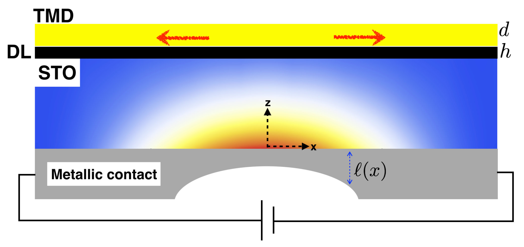 Figure 1
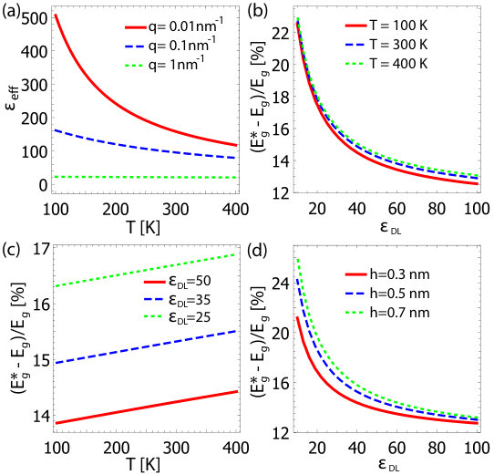 Figure 2
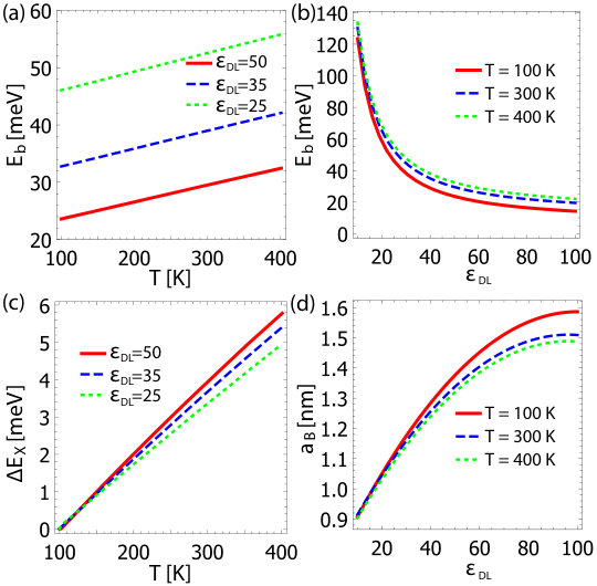 Figure 3
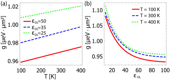 Figure 4
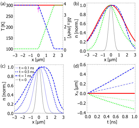 Figure 5
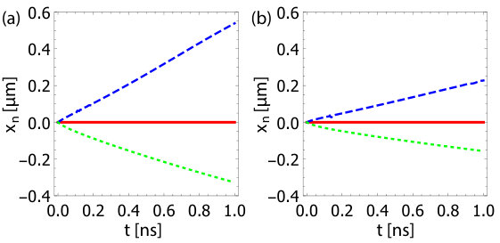 Figure 6
Peer Reviews
No public reviews on file for this paper yet. If you reviewed it on a platform where reviews are public (OpenReview, ICLR, NeurIPS, ICML), you can paste yours below so the community can read it here.
Videos
No videos yet. Explain this paper in a talk, walkthrough, or lecture? Add one.
Exciton routing in the heterostructure of TMD and paraelectrics
V. Shahnazaryan
ITMO University, St. Petersburg 197101, Russia
O. Kyriienko
NORDITA, KTH Royal Institute of Technology and Stockholm University, Roslagstullsbacken 23, SE-106 91 Stockholm, Sweden
ITMO University, St. Petersburg 197101, Russia
H. Rostami
NORDITA, KTH Royal Institute of Technology and Stockholm University, Roslagstullsbacken 23, SE-106 91 Stockholm, Sweden
Abstract
We propose a scheme for the spatial exciton energy control and exciton routing in a transition metal dichalcogenide (TMD) monolayer which lies on a quantum paraelectric substrate. It relies on the ultrasensitive response of the substrate dielectric permittivity to temperature changes, allowing for spatially inhomogeneous screening of Coulomb interaction in a monolayer. As an example, we consider the heterostructure of TMD and strontium titanate oxide SrTiO3, where large dielectric screening can be attained. We study the impact of substrate temperature on the characteristic electronic features of TMD monolayers such as the particle bandgap and exciton binding energy, Bohr radius and nonlinearity (an exciton-exciton interaction). The combination of particle bandgap and exciton binding energy modulation results in the shift of the exciton resonance energy. Applying local heating, we create spatial patterns with varying exciton resonant energy and an exciton flow towards the energetically lower region of the sample.
I Introduction
The synthesis of atomically thin transition metal dichalcogenides (TMDs), such as MoS2 and WS2, opened new horizons for contemporary semiconductor optics Mak2010 ; Novoselov2016 . Thanks to direct band gap and rich diversity of exciton states, caused by the presence of a valley degree of freedom, the family of TMD monolayers becomes especially favorable for addressing a wide range of exciton-related phenomena ChernikovReview . In addition, the TMD monolayers possess giant exciton binding energy of the order of 0.3-0.5 eV, allowing for a room temperature operation. The study of excitonic effects in TMD monolayers covers the spectroscopic measurement Zhao2013 ; Shan2014 ; Zhu2015 ; Shang2015 ; Hill2015 ; Ceballos2016 ; Schmidt2016 ; Chernikov2014 and first principle calculation of binding energy Komsa2012 ; Rama2012 ; Lambrecht2012 ; Yakobson2013 ; Berkelbach2013 ; Qiu2013 ; Komsa2015 ; Qiu2016 , together with analytic calculations of excitonic properties Berghauser2014 ; Glazov2014 ; Wu2015 ; Li2015 .
The electronic properties of all two-dimensional (2D) materials, with TMDs being a prominent example, are extremely sensitive to external probes such as external gating potential, local strain, and substrate effect. This circumstance opens a way to the control of exciton resonant energy, arising via the interplay of modification of both electronic bandgap () and exciton binding energy (). In particular, the screening of inter-particle interactions via electrically injected free charge carriers Chernikov2015 or by the choice of a suitable substrate Ugeda2014 ; Lin2014 ; Raja2017 ; Borghardt2017 ; Hsu2019 can be employed in order to manipulate the exciton energy (). It should be mentioned, that the modification of electronic bandgap () and exciton binding energy () have the same sign and therefore the overall change in the exciton energy, , is mostly compensated. Yet, this cancellation is not perfect, resulting in a significant shift of the exciton resonant energy position of the order of tens of meVs.
A more challenging task is to attain spatially resolved control over exciton energy. One way to reach this was suggested via application of spatially inhomogeneous strain to the monolayer, leading to local modification of the bandgap, and thus creating the energy gradients for quasiparticles throughout the sample Feng_nph_2012 ; Gomez_nl_2013 ; Rostami2015 ; Pablo_prx_2016 . The latter, known as exciton funnel effect, can be favorable for enhancing the efficiency of solar cells.
In this paper, we propose a new method in order to maintain spatial control over exciton resonant energy in TMD monolayers. The method is based on a spatially resolved modulation of Coulomb interaction by means of dielectric environment. For this purpose, we employ quantum paraelectric materials such as SrTiO3 (STO) and KTaO3 (KTO) known for outstanding dielectric properties, as the substrate.
There is a growing interest in exploring the effect of substrate on the electronic and optical properties of 2D materials. Particularly, the heterostructure of STO substrate with graphene Couto_prl_2011 ; Saha_srep_2014 ; Ryu_nl_2017 ; Sahoo_npj_2018 ; Chen_pssrrl_2018 and TMD Zhang_2016 ; Chen_2018 is attracting considerable attention. The large dielectric constant of STO substrate strongly screens the long-range Coulomb interactions inside 2D materials. This property has been already employed in experimental transport studies of graphene/STO heterostructure Couto_prl_2011 ; Chen_pssrrl_2018 . The angle-resolved spectroscopy of graphene on STO demonstrated the temperature-dependent nonlinearity of the energy spectrum, which can be attributed to the modulation of the electron-electron interaction as a function of temperature Ryu_nl_2017 . Recently, it was experimentally shown that single-layer MoS2 can be grown on STO substrate with different interface terminations Chen_2018 . The experimental evidence implies that large triangle-shape flakes MoS2, with up to 10 m side lengths, are attached to STO surface owing to a weak van der Waals interaction Chen_2018 . The experimental measurements show that the photoluminescence efficiency of single-layer MoS2/STO is high enough and this heterostructure could be promising for optoelectronics.
Here, the substrate induced screening is utilized to manipulate the electronic bandgap and characteristic properties of excitons in TMD, e.g. exciton binding energy and Bohr radius. The latter ultimately results in the modulation of exciton lifetime and nonlinearity, caused by exciton-exciton Coulomb interaction. Precisely, we aim to study the effect of spatially inhomogeneous temperature profiles in STO substrate on the exciton properties in TMD. We show that the spatially resolved heating of the substrate results in a corresponding gradient of the exciton energy. The latter plays a role of the drifting force, routing the excitons towards the minimum of exciton resonance energy , whereas typically the exciton transport in TMD monolayers is of diffusive character Kumar2014 ; Mouri2014 ; Yuan2017 ; Kulig2018 ; Cadiz2018 ; Glazov2019 .
The characteristic feature of the quantum paraelectric compounds (e.g. STO) is the strong quantum fluctuations close to the ferroelectric critical point which suppresses the ferroelectric order. Inverse dielectric function of these materials scales as close to the ferroelectric critical point Rowley_np_2014 ; Fujishita_jpsj_2016 . Due to the quantum paraelectric nature of STO at low temperature, its dielectric constant can reach very high values () in a few hundred Kelvin change of temperature. Phenomenologically, one can use the Barrett formula for STO’s dielectric constant above the critical temperature Sawaguchi1962
[TABLE]
where , , K. The strong temperature-dependent dielectric constant of STO substrate has a dramatic impact on the Coulomb interaction between charged particles inside the 2D material. The temperature gradient in STO can be generated in several ways such as local heating by using lasers and Joule heating Watelot_prl_2012 . Particularly, in Ref. Watelot_prl_2012 , it is shown that by utilizing Joule heating in a nanocontact, it is possible to create large temperature gradient, K, within nanoscale depth ( nm). Here, we assume a similar scenario where a desired temperature profile can be achieved in STO by properly designing the thickness of a metallic contact and fabricating a nanocontact. A non-uniform resistivity, , comes as a result of the non-uniform thickness of the metallic nanocontact, . Considering a current flow in the Ohmic nanocontact with an inhomogeneous resistivity, an inhomogeneous temperature can be achieved at the interface of STO and the metallic contact. A schematic illustration of a non-uniform temperature distribution is shown in Fig. 1.
The rest of the paper is organized in three sections. In Sec. II we explain the main body of our modeling. In Sec. III we present our numerical results and corresponding discussion. In Sec. IV we summarize the main achievements of the study, and provide the outlook for future directions.
II Methods
We consider a structure of an atomically thin monolayer of MoS2 deposited on a bulk STO substrate, being a paraelectric material with a giant dielectric constant [see Fig. 1(a)]. The TMD monolayer represents a direct gap semiconductor, which can host excitons at room temperatures. The system can be described as a two-body problem, which satisfies the following Schrodinger equation:
[TABLE]
where , are the electron-hole relative and center of mass (CM) coordinates, and , are exciton total and reduced masses, respectively. For monolayer MoS2 the electron and hole effective masses are and , where is the free electron mass Lambrecht2012 . Here stands for the single-layer bandgap. Evidently, both the bandgap and the exciton binding energy are determined by the Coulomb interaction in the structure. Hence, we first proceed with the analysis of the Coulomb interaction in the system.
Due to the discontinuity of dielectric permittivity at the interfaces of monolayer with substrate and cover layer (or vacuum), the Coulomb interaction substantially differs from the conventional dependence. Typically it is described by the Keldysh-Rytova formula Keldysh ; Cudazzo2011 . However, the material properties of STO impose additional peculiarity to the inter-particle interactions in the considered system. Particularly, it is known that the capacitance of nanoscale STO based capacitors is strongly affected due to the formation of the so-called dead layer at the STO-metal interfaces Spaldin2006 ; Chang2009 . The latter is characterized by much smaller dielectric permittivity, caused by the rearrangement of atoms to compensate the strains on the surface of STO. It is still disputable whether the presence of this layer is inherent property of STO or stems from fabrication imperfections. However, accounting for a dead layer impact allows to provide a more realistic description of such interfaces. In recent experiments with graphene grown on STO substrate it was shown that the STO induced screening is severely quenched Ryu_nl_2017 , which can be attributed to the dielectric constant reduction due to the dead layer. Based on the aforesaid, we model this extra quenching by considering a thin dead layer at the interface of STO/TMD as sketched in Fig. 1(a). The generic interaction potential in Fourier space is given by
[TABLE]
where the bare attractive Coulomb interaction between an electron and a hole reads with as the elementary charge. The effective substrate-induced nonlocal dielectric function reads Florian2018
[TABLE]
where and
[TABLE]
For the shorthand notation in the above formula, we use instead of . Notice that corresponds to the dielectric constant of air; and denote the dielectric constant and the thickness of single-layer TMD. and correspond to the dielectric permittivity and thickness of dead layer. While the exact values of parameters for the dead layer depend on particular experimental realization, we take its width be of the order of 4Å. The dielectric permittivity of the dead layer is shown to be temperature independent Chang2009 and much smaller than that of bulk STO, and we assume it to vary in the range of 10 to 100. Here we also disregard the vertical variation of STO temperature. The latter is explained by the evidence that only a few nm thick upper skin of substrate affects the strength of Coulomb interaction inside the single layer TMD, and the temperature variation on that length scale is negligible.
The parametric dependence of Coulomb interaction on the substrate temperature is reflected in the temperature-induced modulation of STO’s dielectric constant given in Eq. (1). The heat impact on the effective dielectric function is shown in Fig. 2(a). For small values of momentum, , there is a well pronounced dependence of effective permittivity on temperature, mostly determining the excitonic structure. On the other hand, for larger values of , the temperature dependence is negligible, and the value of permittivity is small, meaning a reduced screening of the Coulomb interaction. As we show later, this circumstance leads to strong bandgap renormalization due to Coulomb exchange between particles. It should be also mentioned, that the presence of the dead layer significantly suppresses the impact of STO giant permittivity.
III Results and discussion
In this section we report and discuss our numerical results on the impact of substrate temperature on excitons in single-layer TMD.
III.1 Bandgap renormalization
The modulation of electron-electron interaction strength due to the variation of screening rate can lead to the renormalization of single-particle bandgap in TMD layer. In order to evaluate the strength of bandgap renormalization, we calculate the mean-field self-energy correction to the energy spectrum in TMD. In the low energy limit, the electron Hamiltonian of a single atomic layer takes the following two-band form around the corner of hexagonal Brillouin zone Rostami13a ; Liu13 ; Andor15
[TABLE]
where and , , are the identity matrix and the components of Pauli matrix, respectively. The components of the Hamiltonian (6) read
[TABLE]
where is the chemical potential. Here, , stand for valley and spin degrees of freedom, respectively. Note that , where is the lattice constant of MoS2. The numerical values of this Hamiltonian parameters are taken as eV, eV, meV, meV, meV and the bare bandgap is set as eV based on experimental Ulstrup2016 and theoretical Qiu2013 evidences. The self-consistent mean-field self-energy correction is given by
[TABLE]
Notice that with as the Boltzmann constant, is the fermionic Matsubara frequency, is the electron-electron interaction with a static screening effect and the Green’s function follows
[TABLE]
We seek the self-energy function in the following generic two-band form
[TABLE]
Calculating the Green’s function, performing Matsubara summation over the fermionic frequency, and considering the effective dielectric function given in Eq. (4), one obtains the following self-consistent equations of the self-energy:
[TABLE]
in which we explicitly note the -dependence of the self-energy and stands for the bare Coulomb interaction between two electrons. The approximation in Eq. (11) corresponds to using the approximate values of Fermi-Dirac distribution functions as and for the conduction and valence band, respectively. This assumption is justified owing the large value of the band gap comparing to at room temperature. Note that the term is decoupled from when we use the approximate Fermi-Dirac function. In fact, it is shown that results in an irrelevant rigid energy shift Borghi2009 ; Rostami15b and therefore can be safely dropped. Moreover, we recall that . We introduce an upper momentum cutoff chosen to preserve the total available phase space. Namely, considering the valley degeneracy we set , where is the area of the Brillouin zone. This implies . Eventually, the renormalized bandgap reads
[TABLE]
The results of numerical simulations are shown in Fig. 2. One general observation is that the presence of Coulomb interactions essentially modifies bandgap. Depending on the parameters of the dead layer, the renormalization rate, i.e. , varies in 12-25 range [see Figs. 2 (b), (d)]. In addition, there is a pronounced dependence on the substrate temperature, resulting in change of bandgap of about 15 meV for the temperature variation of 300 K. Our numerical results based on the simple low-energy modeling are in a good agreement with previous sophisticated theoretical analysis and experimental measurements Qiu2013 ; Ugeda2014 .
III.2 The modulation of binding energy
The modulation of the substrate dielectric constant leads to modification of the spatial properties of excitons, which become coordinate-dependent. For a long wavelength temperature profile, we can consider that changes smoothly in space. Therefore, any significant variation happens on the scale of tens of nanometers, while the Coulomb interaction inside the exciton occurs at sub-nm scale. This means that one can safely neglect the modulation of substrate permittivity as a function of exciton relative coordinate, i.e. . The latter allows for the factorization of an exciton wave function in the form , leading to the separation of exciton internal and CM dynamics:
[TABLE]
and
[TABLE]
where is the exciton binding energy. As it follows from Eq. (14), plays a role of the effective potential energy for the exciton CM wavefunction.
We note that Eq. (13) with the potential given by Eq. (3) is not exactly solvable. To characterize the exciton internal state, we employ a variational approach Shahnazaryan2017 , using as a trial function the conventional 2D exciton wavefunction Yang_pra_1991 in momentum space:
[TABLE]
Here, is a variational parameter and its critical value which minimizes the binding energy is the Bohr radius, i.e. . The results of the binding energy calculation as a function of substrate temperature (dielectric permittivity) are presented in Fig. 3(a). One immediate consequence is that the absolute scale of binding energy is much lower than in conventional hexagonal boron nitride (hBN) based setups, where it lies in 500 meV range Hill2015 . The latter arises from the strong screening of interaction, stemming from the enhanced impact of substrate permittivity. It is notable, that while the dead permittivity sufficiently determines the absolute value of exciton binding energy, it almost does not modify temperature dependence. The latter demonstrates of about 10 meV change for binding energy in the corresponding temperature variation range for different values of dead layer permittivity. The values of exciton Bohr radius vary little with temperature, and can be approximated as nm for dead layer permittivity values , respectively. In contrast to binding energy, these values are quite close to exciton Bohr radius in TMD setups on conventional substrates (about 1 nm). The violation of the conventional ratio between exciton energy and Bohr radius is explained by the evidence that the Coulomb interaction generally in TMD based setups and particularly in the considered structure essentially differs from that in dielectrically homogeneous bulk media.
The dependence of exciton binding energy on dead layer permittivity is further revealed in Fig. 3 (b), demonstrating almost an order of magnitude change for dead layer permittivity variation in the range of 10 to 100. The corresponding variation of Bohr radius is depicted in Fig. 3 (d). We also note that the binding energy can be easily fitted using a linear function:
[TABLE]
where the values of and depend on width and permittivity of the dead layer.
III.3 Exciton resonance energy
The temperature dependence of exciton resonant energy shift relative to reference position at K is shown in Fig. 3 (c). The figure illustrates that while the variation of Coulomb interaction strength modifies both bandgap and exciton binding energy in the same direction, there is no exact cancellation between these effects, leading to a significant shift in the exciton resonance energy. The latter opens a way for exciton routing given that a temperature gradient throughout the sample is created. We also note that the obtained result is in qualitative agreement with the recent experimental observations of the exciton resonant energy response on the modulation of dielectric permittivity Lin2014 ; Raja2017 ; Hsu2019 .
III.4 Exciton nonlinearity
We proceed with the calculation of Coulomb interaction between excitons. Strictly speaking, the exact value of inter-exciton interactions (or the nonlinearity) depends on the particular shape of spatial dependence of binding energy, defining the form of exciton CM wave function. However, given by the smooth spatial variation of binding energy, one can assume the exciton-exciton interaction to be defined solely by the wave function describing exciton internal dynamics. Within the scattering theory formalism, the inter-exciton interaction can be presented as a scattering event between two excitons of equal initial momenta, accompanied by momentum transfer from one exciton to another Ciuti1998 . The maximum of interaction appears at zero exchange momenta, and in the explicit form reads Glazov2009 :
[TABLE]
where is the area of the sample. Here we neglect the contribution of direct dipole-dipole interaction, as for TMD monolayers it was shown to be negligibly small Shahnazaryan2017 .
The results of the calculation as a function of temperature are presented in Fig. 4(a). Similar to the binding energy, the interaction rate grows monotonously by increasing the temperature owing to the reduction of screening effect. The presence of dead layer makes the temperature dependence of interaction less pronounced, yet resulting in a few percent changes at 300 range. However, it should be mentioned that in striking difference with the binding energy, the absolute value of exciton-exciton interaction strength is not dramatically modified due to the giant screening by STO substrate. Particularly, considering a single-layer MoS2 deposited on hexagonal boron nitride (hBN) with permittivity , an exciton has the properties of meV, nm, eVm2. Such a behavior of the exciton-exciton interaction constant is in excellent agreement with an earlier performed investigation for WS2 single-layer Shahnazaryan2017 , where it was shown a reduction of interaction strength of 30 in the limit of vanishing screening length, corresponding to giant substrate screening of Coulomb interaction. The small modulation of interaction energy stems from the fact that for relatively larger values of momentum, relevant for the integration in Eq. (17), the temperature dependence of Coulomb is very weak [see Fig. 2(a)]. The panel (b) in Fig. 4 illustrates the dependence of exciton-exciton interaction on the dead layer permitivitty. The moderate change of interaction strength here can be attributed to the counterplay between the reduction of Coulomb interaction for the case of larger screening and the enhancement of exciton Bohr radius.
III.5 Exciton routing
In the following subsection we consider the dynamics of exciton gas in a spatially inhomogeneous medium. For this purpose by means of inhomogeneous heating we create a spatially varying profile of substrate temperature. The latter results in corresponding spatial modulation of the exciton resonance energy. We note here that given by the low exciton mobility and mean free path, Eq. (14) fails to describe the collective motion of the exciton cloud. Instead, the correct description of exciton propagation implies a diffusive treatment Kulig2018 , where the gradient of exciton resonance energy leads to the appearance of a drifting force. In addition, the variation of temperature results in the modulation of diffusion coefficient as well. The diffusion coefficient is linked with the exciton mobility via Einstein relation, . Here, exciton mobility is defined as , where is the average time interval between exciton collisions. For the monolayer MoS2 it is found to be fs Cadiz2018 . Thus, the exciton transport in the considered structure can be described by the following drift-diffusion equation:
[TABLE]
where is the exciton lifetime. The first terms in brackets on the right hand side of Eq. (III.5) stems from the spatial gradient of exciton resonant energy. The second terms correspond to the contribution of Seebeck effect Glazov2019 ; Perea-Causin2019 . The latter drives excitons from hot to cold areas of the structure, thus working in line with the considered routing mechanism. Here the impact of Seebeck mechanism is accounted for in the assumption that the temperature of exciton gas coincides with that of the structure, corresponding to the limit of fast exciton thermalization. It should be mentioned, that the dynamics of exciton propagation can be influenced by the impact of exciton-phonon coupling Glazov2019 , consideration of which however is beyond the scope of the current investigation.
The low-temperature radiative lifetime value for single-layer TMD deposited on an hBN substrate is about 1 ps ChernikovReview . In contrast, at room temperature it can reach up to ns Shi2013 ; Palumno2013 ; Marie2016 . Yet, given the reduced binding energy in the considered structure, one should account for the impact of non-radiative decay channels as well. For numerical simulations, we use the value of ps.
We consider three scenarios of spatial trend of substrate temperature and the corresponding exciton resonance energy relative to the initial excitation spot. These scenarios are depicted in Fig. 5 (a), with an arrow indicating the position of the initial excitation of exciton cloud. For the sake of simplicity we choose linear dependence of the temperature spatial profile, meaning that the first bracket on the right hand side of Eq. (III.5) vanishes. We start with the initial exciton distribution being , where nm, in accordance with relevant experimental conditions Kulig2018 . Figure 5 (b) demonstrates the normalized exciton density spatial distribution at 1ns after initial excitation for different scenarios. In the presence of temperature gradient the combined action of exciton resonant energy difference and Seebeck effect pushes the maximum of the exciton cloud towards a colder area of the sample. 5 (c) illustrates the snapshots of spatial profiles of exciton density at various moments after the initial excitation. The spatial gradient of temperature and exciton resonant energy here correspond to the blue curve in Fig. 5 (a).
Finally, we study the contributions of resonant energy gradient and Seebeck effect due to the temperature gradient to the routing efficiency. Fig. 5 (d) illustrates the temporal evolution of the maximum of exciton distribution position accounting for Seebeck effect (thick lines) and in the absence of it (thin lines). In principle a scenario when the Seebeck effect is absent can be realized when the gradient of exciton resonant energy is created by means of inhomogeneous strain of substrate rather than temperature gradient. However this task is beyond the scope of current paper and is left for future investigations. As it follows from Fig. 5 (d), the presence of Seebeck effect essentially enhances the efficiency of routing.
IV conclusion
In conclusion, we studied the impact of a paraelectric substrate (using strontium titanate, SrTiO3 as an example) on the excitonic properties of a TMD (e.g. MoS2) monolayer. It was found that the giant screening of Coulomb interaction leads to sufficient bandgap renormalization and quenching of the exciton binding energy. The pronounced dependence of SrTiO3 permittivity on temperature allows for rigid manipulation of exciton resonance energy in a single layer. By applying inhomogeneous heating, it is possible to create a prominent gradient of substrate temperature on the scale of tens of nanometers, directly mapped to the exciton resonant energy. The latter opens a possibility to create controllable exciton currents, having significant potential for exciton transport-based applications. Finally, we note that the proposed effect of exciton routing can be essentially enhanced for the case of strong light-matter coupling regime, leading to the formation of exciton-polaritons Dufferwiel2017 ; Lundt2017 . The ultra-small effective mass of the latter, stemming from the photonic counterpart, would enhance the particle mobility by several orders, allowing to span the routing distance to tens and hundreds of m.
Acknowledgements
The authors are grateful to I. Chestnov, A. Balatsky and I. Shelykh for valuable discussions. The work was supported by VILLUM FONDEN via the Center of Excellence for Dirac Materials (Grant No. 11744). H.R. acknowledges the support from the Swedish Research Council (VR 2018-04252). V.S. acknowledges the support from Goszadanie No. 3.2614.2017/4.6 and Megagrant 14.Y26.31.0015 of the ministry of education and science of Russian Federation, and RFBR Grant No. 18-32-00873. The work was partly supported by the Government of the Russian Federation through the ITMO Fellowship and Professorship Program.
The reference list from the paper itself. Each links out to its DOI / PubMed record.
- 1(1) K. F. Mak, C. Lee, J. Hone, J. Shan, and T. F. Heinz, Phys. Rev. Lett. 105 , 136805 (2010) .
- 2(2) K. S. Novoselov, A. Mishchenko, A. Carvalho, and A. H. C. Neto, Science 353 , 461 (2016) .
- 3(3) G. Wang, A. Chernikov, M. M. Glazov, T. F. Heinz, X. Marie, T. Amand, and B. Urbaszek, Rev. Mod. Phys. 90 , 021001 (2018) .
- 4(4) W. Zhao, Z. Ghorannevis, L. Chu, M. Toh, C. Kloc, P.-H. Tan, and G. Eda, ACS Nano 7 , 791 (2013) .
- 5(5) K. He, N. Kumar, L. Zhao, Z. Wang, K. F. Mak, H. Zhao, and J. Shan, Phys. Rev. Lett. 113 , 026803 (2014) .
- 6(6) B. Zhu, X. Chen, and X. Cui, Sci. Rep. 5 , 9218 (2015) .
- 7(7) J. Shang, X. Shen, C. Cong, N. Peimyoo, B. Cao, M. Eginligil, and T. Yu, ACS Nano 9 , 647 (2015) .
- 8(8) H.M. Hill, A.F. Rigosi, C. Roquelet, A. Chernikov, T.C. Berkelbach, D.R. Reichman, M.S. Hybertsen, L.E. Brus, and T.F. Heinz, Nano Lett. 15 , 2992 (2015) .