Laser slicing: a thin film lift-off method for GaN-on-GaN technology
Vladislav Voronenkov, Natalia Bochkareva, Ruslan Gorbunov, Andrey, Zubrilov, Viktor Kogotkov, Philipp Latyshev, Yuri Lelikov, Andrey Leonidov,, Yuri Shreter

TL;DR
This paper introduces a laser slicing technique using femtosecond laser pulses to lift off thin GaN films with device structures from bulk substrates, enabling transfer onto other substrates without special release layers.
Contribution
The study demonstrates a novel laser slicing method for GaN that does not require release layers, facilitating efficient film transfer for device applications.
Findings
Successful lift-off of 5 μm GaN films with LED structures
Electroluminescence demonstrated post-transfer
No special release layers needed for the process
Abstract
A femtosecond laser focused inside bulk GaN was used to slice a thin GaN film with an epitaxial device structure from a bulk GaN substrate. The demonstrated laser slicing lift-off process did not require any special release layers in the epitaxial structure. GaN film with a thickness of 5 m and an InGaN LED epitaxial device structure was lifted off a GaN substrate and transferred onto a copper substrate. The electroluminescence of the LED chip after the laser slicing lift-off was demonstrated.
Click any figure to enlarge with its caption.
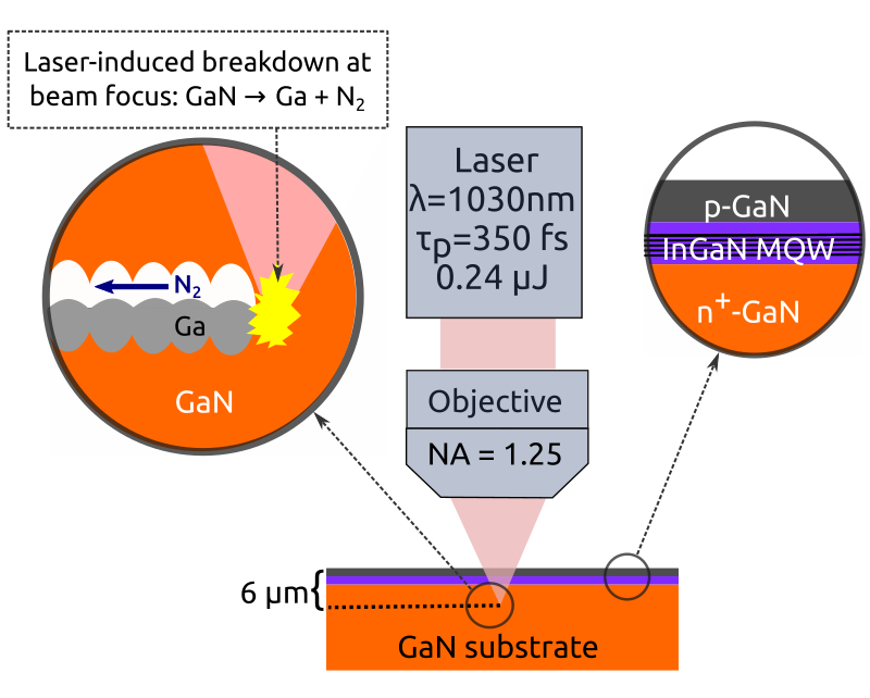 Figure 1
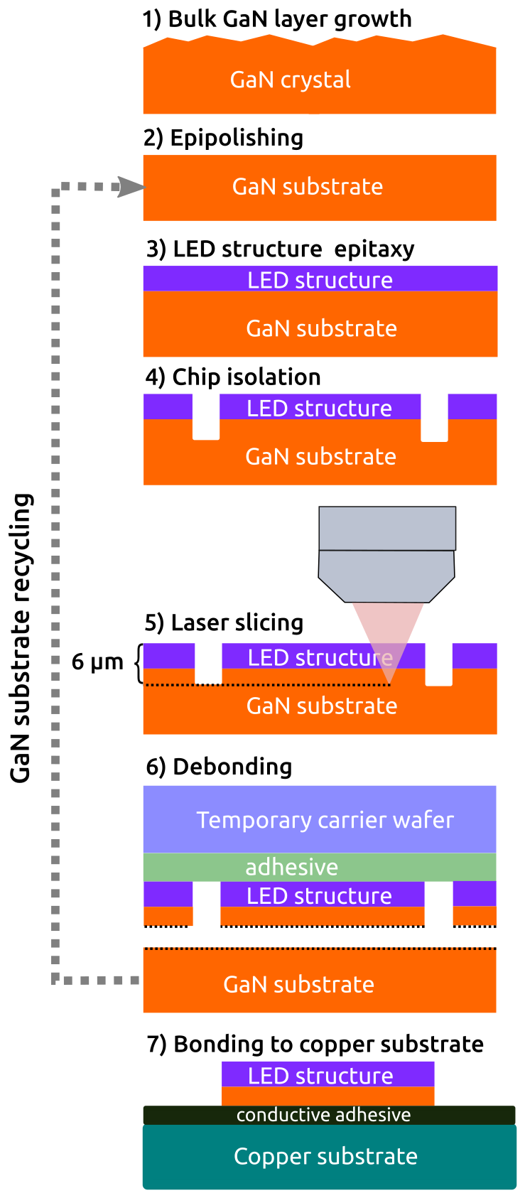 Figure 2
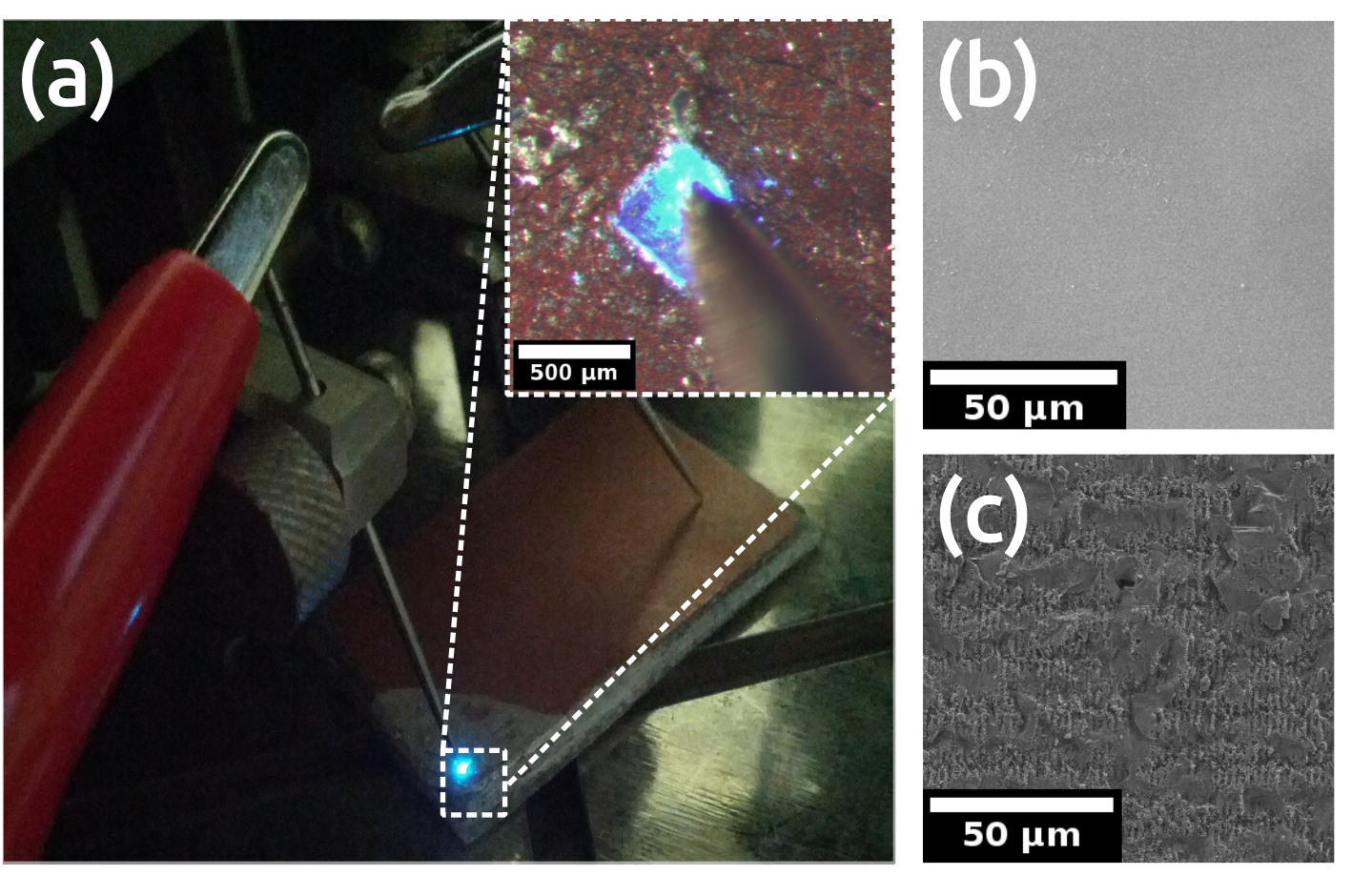 Figure 3
Peer Reviews
No public reviews on file for this paper yet. If you reviewed it on a platform where reviews are public (OpenReview, ICLR, NeurIPS, ICML), you can paste yours below so the community can read it here.
Videos
No videos yet. Explain this paper in a talk, walkthrough, or lecture? Add one.
Laser slicing: a thin film lift-off method for GaN-on-GaN technology
Vladislav Voronenkov1,2
Natalia Bochkareva2
Ruslan Gorbunov1,2
Andrey Zubrilov1,2
Viktor Kogotkov1
Philipp Latyshev1
Yuri Lelikov1,2
Andrey Leonidov1
Yuri Shreter1,2
1TRINITRI-Technology LLC, St Petersburg 194223, Russia
2Ioffe Institute, St Petersburg 194021, Russia
Abstract
A femtosecond laser focused inside bulk GaN was used to slice a thin GaN film with an epitaxial device structure from a bulk GaN substrate. The demonstrated laser slicing lift-off process did not require any special release layers in the epitaxial structure. GaN film with a thickness of 5 m and an InGaN LED epitaxial device structure was lifted off a GaN substrate and transferred onto a copper substrate. The electroluminescence of the LED chip after the laser slicing lift-off was demonstrated.
laser slicing; lift-off; InGaN LED; GaN-on-GaN
Bulk GaN substrate is a crucial element in the production of reliable, high-current density GaN-based devices. However, the widespread use of GaN substrates is currently limited due to their high cost. Separation of the epitaxial device structure from the bulk GaN substrate allows the reuse of the expensive substrate multiple times and thus reduces the effective cost. Also, the separation of the epitaxial structure is necessary to create heterogeneously integrated devices heterogeneous-gan-cmos-2009 ; HETEROGENEOUS-LED-2015 ; HETEROGENEOUS-2010 , as well as to improve heat dissipation DIAMOND-HEMT-2014-Kuball ; HETEROGENEOUS-LED-2015 and light extraction LLO-InGaN-AKASAKI2014 .
To lift-off GaN films from foreign substrates multiple methods were developed: laser lift-off LLO-Kelly-1996 ; natural stress-induced separation Natural-Stress-Moustakas2007 ; YAMANE20121 ; controlled spalling SPALLING-sapphire-LEDbedell-sadana-2013 ; chemical etching of ZnO CLO-ZnO-Rogers2007 , Ga2O3 CLO-TsaiGa2o3-2011 , CrN CLO-CrN-2008-Yao , AlN CLO-AlN-2010-ChengFengLin and Nb2N nb2n-lift-off-2016 sacrificial layers; doping-selective electrochemical etching CLO-nPlus-SiGaN-2009-Park ; substrate removal by grinding or etching melnik_nikolaev_nikitina_vassilevski_dmitriev_1997 ; ETCHING-GaAs-sumitomo-2001 ; Si-wafer-remove-Lesecq-2011 ; Mikulik-Si-etching-2013 ; void-assisted separation USUI-VAS-2003 ; growth over patterned masks gogova2004elog ; HENNIG2008911-WSiN-ELOG ; lipski2010fabrication ; AMILUSIK201399 ; the use of weakly bonded release layers like graphene Graphene-IBM-kim2014principle , BN BN-kobayashi2012layered , carbon CARBON-Phil-2016 ; and the use of substrates with easy cleavage along the c-plane of a GaN epilayer Ga2O3-lift-off-Gogova2012 ; SCAM-Matsuoka-2017 .
To separate a GaN film from a native GaN substrate several approaches were proposed: chemical lift-off process InGaN-GaN-PEC-Youtsey2017 ; porous release layers created by chemical LEE-KOH-POROUS-ETCH , electrochemical Mynbaeva-porous-liftoff ; porous-lif-off-2013 or dry H2-porous-etching-YEH2011 etching of GaN substrate; controlled spalling SPALLING-bedell-sadana2017 ; laser lift-off with an InGaN release layer LLO-InGaN-AKASAKI2014 ; ion implantation Smart-Cut-GaN-Tauzin2005 ; Moutanabbir2010-ion-cleaving ; Ion-Cut-Samsung-2013 ; huang2018defects ; and free-carrier-absorption laser lift-off FCA-LLO-Virko2016 .
The lift-off methods based on the use of an intermediate layer require a complicated epitaxy process. The ion implantation method does not allow separating epitaxial device structures due to a large number of point defects formed by the implantation process Ion-Cut-Samsung-2013 ; He-ion-damage-HAN2017 ; huang2018defects . The free-carrier-absorption LLO method is limited to separating undoped films from a heavily doped substrate FCA-LLO-Virko2016 .
We have proposed a laser slicing lift-off (LSLO) method for separating an epitaxial structure from a bulk GaN substrate, one that does not require any special release layers and can be used both for lifting off pure GaN films and for lifting off GaN films with device structure shreter2013method . The method is based on the effect of GaN decomposition induced by an ultra-short laser pulse focused inside a bulk GaN material. The use of femtosecond lasers is preferable as it allows to reduce the heat-affected zone and the corresponding damage in the surrounding material stuart1996-ns-to-fs . This effect was earlier used to create hollow 3D-channels inside bulk GaN FS-GaN-MACHINING-MIDORIKAWA-2009 and to dice transparent wafers with laser stealth dicing technology LSD-Kumagai-2007 .
The principle of the LSLO method is as follows. To lift-off a thin GaN film with an InGaN multiple quantum well (MQW) device structure from a bulk GaN substrate, the pulses of a near-infrared femtosecond laser are focused inside the GaN layer, several microns under the surface (fig.1). The laser photon energy is less than the InGaN bandgap, so both the InGaN device structure and the GaN substrate are transparent at the wavelength of the laser. The laser pulse energy is adjusted so that the nonlinear breakdown threshold is exceeded only in the focus area and the GaN material in this area is decomposed. Scanning of the focus position is performed in the --plane until a continuous layer of decomposed material is created inside the wafer.
In this work, a proof-of-concept LED chip fabrication using the LSLO method is described. First, a 5-m thick GaN film with an InGaN LED structure was grown homoepitaxially on a bulk GaN layer. After that, the film with the LED structure was lifted-off from the substrate and transferred to a copper carrier (fig. 2). The electroluminescence of the LED chip after the lift-off was demonstrated. A detailed study of the LED chip for possible damage caused by the LSLO process will be published separately.
A GaN-on-sapphire HVPE template was employed as a bulk-like substrate for the InGaN LED structure epitaxy. The template was grown on a 2-inch c-plane (0001) sapphire substrate using a two-stage growth process voronenkov2013two . The thickness of the bulk-like HVPE GaN layer was 50 m. The surface of the HVPE GaN template was epi-polished by a chemical-mechanical polishing process. After that, the InGaN MQW LED structure was deposited using a metal-organic chemical vapor deposition system. The LED structure consisted of a 5-m thick doped GaN:Si (= cm*-3*) layer; five pairs of InGaN quantum wells with a well width of 2.3 nm and a barrier width of 11 nm; and a 0.3-m thick p-doped GaN:Mg layer (p= cm*-3*).
The chip isolation and the LSLO process were performed with an ytterbium-doped, diode-pumped solid-state laser with a wavelength of 1030 nm, a pulse duration of 350 fs, and a pulse energy of 400 J. A three-axis motorized translation stage was used to perform scanning in the --plane and to adjust the focus position along the axis.
First, a 500m500m chip was isolated through the laser scribing process – grooves with a depth of 6 m and a width of 5 m were cut along the chip perimeter. Such grooves are necessary to release the gas produced by the GaN decomposition during the LSLO process. A 20 dry objective was used to focus the laser beam on the surface of the GaN layer. The pulse energy was 5 J, pulse repetition rate was 1 kHz and the scanning velocity was 1000 m/s.
To perform the LSLO an oil immersion objective (100, NA = 1.25) with an = immersion oil was used. Before performing the LSLO, the breakdown threshold was determined: the laser was focused at a depth of 6 m below the surface and the laser pulse energy was gradually increased until a breakdown in the focus area was observed at a pulse energy of 0.2 J. After that, the LSLO was performed using a pulse energy of 0.24 J. The laser beam, directed from the front side of the sample with a beam focus located 6 m under the surface was used to create a thin decomposed layer 6 m below the surface of the wafer. The scanning pattern exhibited a set of parallel rows. The scanning velocity along the row was 1000 m/s and the pulse repetition rate was 2.5 kHz resulting in a pulse-to-pulse distance along the row of 0.4 m; the distance between the rows was 2 m.
After the LSLO process, the LED chip was bonded to a temporary carrier wafer using a cyanoacrylate adhesive. After the adhesive hardened, the chip was debonded from the substrate. Then, the cyanoacrylate adhesive was dissolved, and the chip was bonded to a copper substrate using an electrically conductive silver epoxy as a bonding material.
To observe the electroluminescence of the chip, an electrical current probe was connected directly to the surface of the chip, without applying any current-spreading layers. The light emitting image of the LED chip on a copper substrate is shown in fig. 3(a). The operating current was 1 mA. Blue-light emission was observed under the probe, confirming that the MQW LED structure was not destroyed during the LSLO process. A detailed study of the I-V characteristics and the electroluminescence spectrum, as well as a detailed comparison of the LED performance before and after the LSLO process will be published separately.
The SEM image of the top side (Ga-face) of the LED chip after the LSLO process is shown in fig. 3(b). No signs of damage caused by the LSLO were observed on the surface. The SEM image of the bottom side (nitrogen-face) of the LED chip after LSLO and debonding is shown in fig. 3(c). The remains of the decomposed layer were observed. The surface roughness of the bottom side of the chip was estimated using a tilted-view SEM image (not shown) to be about 1m, which corresponds to the focus depth of the laser beam. The thickness of the separated film was measured using a side-view SEM image (not shown) and was 5 m, which corresponds to the position of the focus below the surface.
Following is a brief discussion of the technological limits and possible improvements of the method. The maximum thickness of the lifted-off layer is limited by the defocusing of the laser beam caused by spherical aberration and optical inhomogeneity of the material. Recent advances in the growth of pure GaN SCIOCS-2017-pure make it possible to obtain an optically homogeneous material, and the adaptive optics techniques can compensate for spherical aberration when focusing to a depth of hundreds of microns Salter-2014-depth . The minimum thickness of the decomposed layer is limited by the depth of focus of the laser beam, which can be reduced by the use of high-numerical-aperture objectives, such as solid immersion lenses SIL-Kino-1999 . Processing throughput is mainly limited by the scanning speed, therefore the use of parallel multi-beam machining methods Kato-2005-microlens ; Booth-2010-parallel is highly desirable. Wafers with already deposited metallization layers can also be processed. For this, the focused laser beam is directed from the underside of the wafer. Other materials that decompose irreversibly under the action of laser breakdown can also be processed. The greatest practical interest of such materials is diamond, which is graphitized by laser breakdown Konov-2008-diamond .
In conclusion, a 5-m thick GaN film with the InGaN LED MQW structure was lifted off from the bulk GaN layer by focusing near-infrared femtosecond laser pulses 6 m under the surface of the GaN wafer. The film was transferred to a copper carrier and the electroluminescence of the LED structure was demonstrated.
Acknowledgements.
The authors gratefully thank Dr. I. Guiney and Prof. C. Humphreys from Cambridge University for the InGaN LED structure growth.
The reference list from the paper itself. Each links out to its DOI / PubMed record.
- 1(1) J. W. Chung, J. Lee, E. L. Piner, and T. Palacios, “Seamless On-Wafer Integration of Si(100) MOSFE Ts and Ga N HEM Ts,” IEEE Electron Device Letters , vol. 30, no. 10, pp. 1015–1017, Oct 2009. [Online]. Available: https://doi.org/10.1109/LED.2009.2027914 · doi ↗
- 2(2) A. J. Trindade, B. Guilhabert, E. Y. Xie, R. Ferreira, J. J. D. Mc Kendry, D. Zhu, N. Laurand, E. Gu, D. J. Wallis, I. M. Watson, C. J. Humphreys, and M. D. Dawson, “Heterogeneous integration of gallium nitride light-emitting diodes on diamond and silica by transfer printing,” Opt. Express , vol. 23, no. 7, pp. 9329–9338, Apr 2015. [Online]. Available: http://doi.org/10.1364/OE.23.009329 · doi ↗
- 3(3) O. Moutanabbir and U. Gosele, “Heterogeneous Integration of Compound Semiconductors,” Annual Review of Materials Research , vol. 40, no. 1, pp. 469–500, 2010. [Online]. Available: http://doi.org/10.1146/annurev-matsci-070909-104448 · doi ↗
- 4(4) J. W. Pomeroy, M. Bernardoni, D. C. Dumka, D. M. Fanning, and M. Kuball, “Low thermal resistance Ga N-on-diamond transistors characterized by three-dimensional Raman thermography mapping,” Applied Physics Letters , vol. 104, no. 8, p. 083513, 2014. [Online]. Available: https://doi.org/10.1063/1.4865583 · doi ↗
- 5(5) D. Iida, S. Kawai, N. Ema, T. Tsuchiya, M. Iwaya, T. Takeuchi, S. Kamiyama, and I. Akasaki, “Laser lift-off technique for freestanding Ga N substrate using an In droplet formed by thermal decomposition of Ga In N and its application to light-emitting diodes,” Applied Physics Letters , vol. 105, no. 7, p. 072101, 2014. [Online]. Available: http://doi.org/10.1063/1.4893757 · doi ↗
- 6(6) M. K. Kelly, O. Ambacher, R. Dimitrov, R. Handschuh, and M. Stutzmann, “Optical Process for Liftoff of Group III-Nitride Films,” physica status solidi (a) , vol. 159, no. 1, pp. R 3–R 4, 1996. [Online]. Available: http://doi.org/10.1002/1521-396X(199701)159:1%3CR 3::AID-PSSA 99993%3E 3.0.CO;2-F · doi ↗
- 7(7) A. D. Williams and T. Moustakas, “Formation of large-area freestanding gallium nitride substrates by natural stress-induced separation of Ga N and sapphire,” Journal of Crystal Growth , vol. 300, no. 1, pp. 37 – 41, 2007, first International Symposium on Growth of Nitrides. [Online]. Available: https://doi.org/10.1016/j.jcrysgro.2006.10.224 · doi ↗
- 8(8) K. Yamane, M. Ueno, H. Furuya, N. Okada, and K. Tadatomo, “Successful natural stress-induced separation of hydride vapor phase epitaxy-grown Ga N layers on sapphire substrates,” Journal of Crystal Growth , vol. 358, pp. 1 – 4, 2012. [Online]. Available: https://doi.org/10.1016/j.jcrysgro.2012.07.038 · doi ↗