Free-standing 2-inch bulk GaN crystal fabrication by HVPE using a carbon buffer layer
Vladislav Voronenkov, Andrey Leonidov, Natalia Bochkareva, Ruslan, Gorbunov, Philippe Latyshev, Yuri Lelikov, Viktor Kogotkov, Andrey Zubrilov, and Yuri Shreter

TL;DR
This paper reports a method for fabricating free-standing 2-inch bulk GaN crystals using HVPE with a carbon buffer layer, enabling self-separation from the substrate and resulting in high-quality crystals.
Contribution
It introduces a novel HVPE process with an in situ carbon buffer layer for producing large, free-standing GaN crystals with low dislocation density.
Findings
Achieved 365 μm thick, 50 mm diameter free-standing GaN crystals.
Dislocation density of 8×10^6 cm^-2.
X-ray rocking curve FWHM of 164 arcsec indicating high crystal quality.
Abstract
A free-standing bulk gallium nitride layer with a thickness of 365 m and a diameter of 50 mm was obtained by hydride vapor phase epitaxy on a sapphire substrate with a carbon buffer layer. The carbon buffer layer was deposited by thermal decomposition of methane in the same process with the growth of a bulk GaN layer. The bulk GaN layer grown on the carbon buffer layer self-separated from the sapphire substrate during the cooling after the growth. The dislocation density was cm. The (0002) X-Ray rocking curve full width at half maximum was 164 arcsec.
Click any figure to enlarge with its caption.
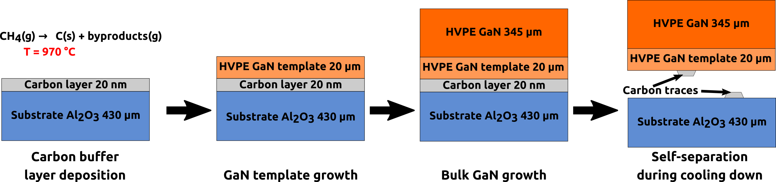 Figure 1
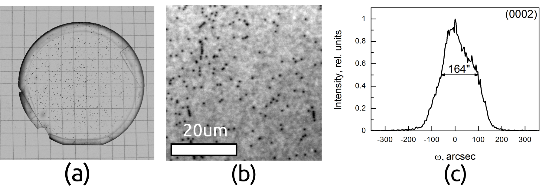 Figure 2
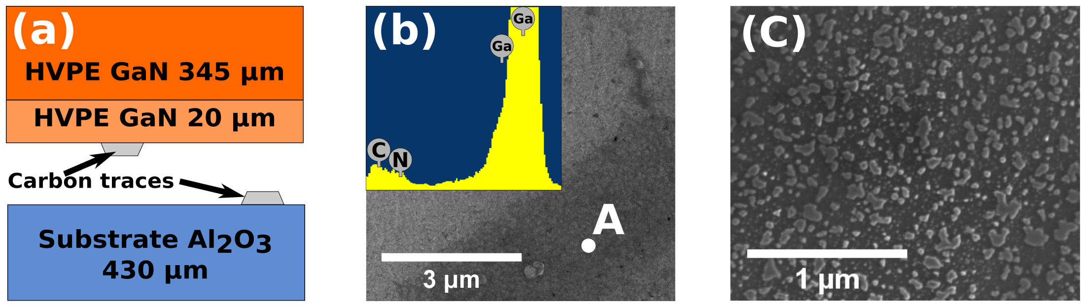 Figure 3
Peer Reviews
No public reviews on file for this paper yet. If you reviewed it on a platform where reviews are public (OpenReview, ICLR, NeurIPS, ICML), you can paste yours below so the community can read it here.
Videos
No videos yet. Explain this paper in a talk, walkthrough, or lecture? Add one.
Free-standing 2-inch bulk GaN crystal fabrication by HVPE using a carbon buffer layer
Vladislav Voronenkov1,2
Andrey Leonidov3
Natalia Bochkareva1
Ruslan Gorbunov1,2
Philippe Latyshev4
Yuri Lelikov1,2
Viktor Kogotkov2
Andrey Zubrilov1,2 and Yuri Shreter1,2
1Ioffe Institute, Politehnicheskaya 26, St. Petersburg, 194021, Russia
2TRINITRI-Technology LLC, 194223, St. Petersburg, Russia
3Peter the Great St. Petersburg Polytechnic University, Politehnicheskaya 29, St. Petersburg, 195251, Russia
4OOO NTS, 197198, St. Petersburg, Russia [email protected]
Abstract
A free-standing bulk gallium nitride layer with a thickness of 365 m and a diameter of 50 mm was obtained by hydride vapor phase epitaxy on a sapphire substrate with a carbon buffer layer. The carbon buffer layer was deposited by thermal decomposition of methane in situ in the same process with the growth of a bulk GaN layer. The bulk GaN layer grown on the carbon buffer layer self-separated from the sapphire substrate during the cooling after the growth. The dislocation density was cm*-2*. The (0002) X-Ray rocking curve full width at half maximum was 164 arcsec.
1 Introduction
Today, HVPE heteroepitaxial growth of GaN on foreign substrates is the main method for commercial production of GaN substrates. An important step in this technology is the separation of the bulk GaN layer from the substrate after the growth process. Thick GaN layers with thicknesses of several hundred microns typically separate from sapphire substrates during the cooling after the growth, but this self-separation process is accompanied by cracking of the GaN layer [1, 2, 3]. The cracking of a GaN layer can be suppressed by growing a bulk GaN layer with a thickness of several millimeters, or by reducing the bonding energy between a substrate and a GaN layer. Different methods were proposed to reduce the bonding energy between a substrate and a GaN layer, including porous layers created by dry etching [4], wet etching [5], electrochemical etching [6] or GaN decomposition induced by a TiN mask [7]; epitaxial lateral overgrowth over dielectric masks [8, 9, 10, 11], employing substrates with a cleavage plane parallel to the c-axis of GaN [12, 13], and weakly bonded buffer layers [14, 15]. All these methods either require using non-standard substrates [12, 13] or special ex situ pre-growth processing of the substrate like etching, buffer layer deposition, dielectric or metal mask fabrication, or GaN template structure growth.
Carbon in the form of graphite is a promising material for creating buffer layers that facilitate self-separation due to the hexagonal symmetry of the crystal lattice and a low interlayer binding energy [16]. Earlier, a nanocrystalline graphite carbon buffer layer deposited by PECVD on a sapphire substrate was used for GaN growth and self-separation. A 200-m thick GaN layer was grown and free-standing GaN pieces were obtained [17]. In this work, a bulk GaN layer with a thickness of 365 m was grown on a sapphire substrate with a carbon buffer layer deposited in situ, and a wafer-scale self-separation has been demonstrated (figure 1).
2 Experimental details
The experiment used a standard epi-polished 2-inch sapphire substrate with a thickness of 430 m and a crystallographic orientation of (0001) with a miscut of 0.5*∘* towards the m-plane.
A carbon buffer layer and a GaN film with a thickness of 20 m were grown in a multi-wafer HVPE reactor with an installed methane supply line. The design of the reactor limited the maximal GaN layer thickness to 200 m; therefore, to grow the bulk layer, the structure was transferred to the vertical HVPE reactor optimized for the bulk layer deposition.
A carbon layer was deposited using the methane thermal decomposition process from a CH4/H2 mixture [18] at a deposition temperature of 1020 *∘*C, a total process pressure of 105 kPa and a methane partial pressure of 1.3 kPa. The deposition rate was 10 nm/min. After that, a 20-m thick GaN layer was deposited at a temperature of 960 *∘*C. Then, the structure was cooled down and transferred to a vertical HVPE reactor where a 345-m thick GaN layer was grown at a growth rate of 100 m/h, a V/III ratio of 35, a total reactor pressure of 15 kPa, and a substrate temperature ramping from 880 *∘*C at the beginning of the growth process to 920 *∘*C at the end of the growth process. Self-separation induced by thermal stress occurred during the cooling down after the growth process, and a single piece GaN layer with a thickness of 365 m and a diameter of 50 mm was obtained.
3 Results and discussion
A photograph of a free-standing GaN layer is shown in figure 2(a). The surface of the layer is smooth, the V-shaped pit density is 40 cm*-2*, and the opening angle of V-shaped pits is in the range of 80*∘-100∘* that is typical for GaN layers grown in the low-temperature mode [19].
The (0002) XRD rocking curve of the Ga face of the free-standing GaN is shown in figure 2(c). The FWHM value is 164 arcsec. The lattice curvature radius of free-standing GaN measured by XRD is 3.1 m. The residual bow is typical for free-standing GaN layers obtained by heteroepitaxy and is a result of a built-in strain caused by defect density gradients along the c-axis of a GaN layer [20, 21] and by the inclination of threading dislocations [22].
The threading dislocation density on the Ga-face surface of the free-standing GaN layer was estimated to be cm*-2* (figure 2(b)), which is typical for GaN layers with thicknesses of 350-400 m, grown on a sapphire substrate [23]. The estimation was made by measuring the dark spot density using the cathodoluminescent microscopy [24].
The surfaces of the N-face of the GaN layer and the sapphire substrate were smooth and mirror-like. Both these surfaces were examined by scanning electron microscopy combined with energy-dispersive X-ray spectroscopy. The carbon buffer layer remnants were found on the N-face of free-standing GaN layer (figure 3(b)) and the sapphire substrate surfaces (not shown). This confirms that the self-separation occurred strictly along the carbon buffer layer. The sapphire substrate surface was covered by submicron-sized irregularities (figure 3(c)), while no irregularities of the same scale were observed on the GaN surface. A possible origin of such irregularities could be the reduction of sapphire by carbon [25]. Sapphire etching and the resulting cavity formation may also lower the bonding energy between a GaN layer and a substrate and facilitate the self-separation process.
4 Conclusion
A bulk GaN layer was epitaxially grown on a sapphire substrate with a carbon buffer layer. The layer spontaneously separated from the substrate along the carbon buffer layer during the cooling down process, and a free-standing GaN layer with a diameter of 50 mm and a thickness of 365 m was obtained. The surface morphology and crystalline structure of the free-standing GaN layer did not degrade compared to a GaN layer grown on a bare sapphire substrate in similar conditions.
5 Acknowledgments
The authors gratefully thank O. Mededev and O. Vyvenko from St. Petersburg State University for help with microscopic investigations.
References
- [1]
A. D. Williams and T. Moustakas, “Formation of large-area freestanding gallium nitride substrates by natural stress-induced separation of GaN and sapphire,” Journal of Crystal Growth, vol. 300, no. 1, pp. 37 – 41, 2007, first International Symposium on Growth of Nitrides. [Online]. Available: https://doi.org/10.1016/j.jcrysgro.2006.10.224
- [2]
K. Yamane, M. Ueno, H. Furuya, N. Okada, and K. Tadatomo, “Successful natural stress-induced separation of hydride vapor phase epitaxy-grown GaN layers on sapphire substrates,” Journal of Crystal Growth, vol. 358, pp. 1 – 4, 2012. [Online]. Available: https://doi.org/10.1016/j.jcrysgro.2012.07.038
- [3]
H. Ashraf, R. Kudrawiec, J. Weyher, J. Serafinczuk, J. Misiewicz, and P. Hageman, “Properties and preparation of high quality, free-standing GaN substrates and study of spontaneous separation mechanism,” Journal of Crystal Growth, vol. 312, no. 16, pp. 2398 – 2403, 2010. [Online]. Available: https://doi.org/10.1016/j.jcrysgro.2010.05.004
- [4]
Y.-H. Yeh, K.-M. Chen, Y.-H. Wu, Y.-C. Hsu, T.-Y. Yu, and W.-I. Lee, “Hydrogen etching of GaN and its application to produce free-standing GaN thick films,” Journal of Crystal Growth, vol. 333, no. 1, pp. 16 – 19, 2011. [Online]. Available: https://doi.org/10.1016/j.jcrysgro.2011.08.022
- [5]
C.-Y. Lee, Y.-P. Lan, P.-M. Tu, S.-C. Hsu, C.-C. Lin, H.-C. Kuo, G.-C. Chi, and C.-Y. Chang, “Natural substrate lift-off technique for vertical light-emitting diodes,” Applied Physics Express, vol. 7, no. 4, p. 042103, 2014. [Online]. Available: https://doi.org/10.7567/APEX.7.042103
- [6]
M. G. Mynbaeva, A. E. Nikolaev, A. A. Sitnikova, and K. D. Mynbaev, “HVPE homo-epitaxial growth of GaN on porous substrates,” CrystEngComm, vol. 15, pp. 3640–3646, 2013. [Online]. Available: http://dx.doi.org/10.1039/C3CE27099H
- [7]
Y. Oshima, T. Eri, M. Shibata, H. Sunakawa, K. Kobayashi, T. Ichihashi, and A. Usui, “Preparation of Freestanding GaN Wafers by Hydride Vapor Phase Epitaxy with Void-Assisted Separation,” Japanese Journal of Applied Physics, vol. 42, no. 1A, p. L1, 2003. [Online]. Available: https://doi.org/10.1143/JJAP.42.L1
- [8]
D. Gogova, A. Kasic, H. Larsson, C. Hemmingsson, B. Monemar, F. Tuomisto, K. Saarinen, L. Dobos, B. Pécz, P. Gibart, and B. Beaumont, “Strain-free bulk-like GaN grown by hydride-vapor-phase-epitaxy on two-step epitaxial lateral overgrown GaN template,” Journal of Applied Physics, vol. 96, no. 1, pp. 799–806, 2004. [Online]. Available: https://doi.org/10.1063/1.1753073
- [9]
F. Lipski, T. Wunderer, S. Schwaiger, and F. Scholz, “Fabrication of freestanding 2”-GaN wafers by hydride vapour phase epitaxy and self-separation during cooldown,” Physica Status Solidi (a), vol. 207, no. 6, pp. 1287–1291, 2010. [Online]. Available: https://doi.org/10.1002/pssa.200983517
- [10]
C. Hennig, E. Richter, M. Weyers, and G. Trankle, “Freestanding 2-in GaN layers using lateral overgrowth with HVPE,” Journal of Crystal Growth, vol. 310, no. 5, pp. 911 – 915, 2008, proceedings of the E-MRS Conference, Symposium G. [Online]. Available: https://doi.org/10.1016/j.jcrysgro.2007.11.102
- [11]
M. Amilusik, T. Sochacki, B. Lucznik, M. Bockowski, B. Sadovyi, A. Presz, I. Dziecielewski, and I. Grzegory, “Analysis of self-lift-off process during HVPE growth of GaN on MOCVD-GaN/sapphire substrates with photolitographically patterned Ti mask,” Journal of Crystal Growth, vol. 380, pp. 99 – 105, 2013. [Online]. Available: https://doi.org/10.1016/j.jcrysgro.2013.06.005
- [12]
K. Kachel, M. Korytov, D. Gogova, Z. Galazka, M. Albrecht, R. Zwierz, D. Siche, S. Golka, A. Kwasniewski, M. Schmidbauer, and R. Fornari, “A new approach to free-standing GaN using -Ga2O3 as a substrate,” CrystEngComm, vol. 14, pp. 8536–8540, 2012. [Online]. Available: http://dx.doi.org/10.1039/C2CE25976A
- [13]
K. Ohnishi, M. Kanoh, T. Tanikawa, S. Kuboya, T. Mukai, and T. Matsuoka, “Halide vapor phase epitaxy of thick GaN films on ScAlMgO4 substrates and their self-separation for fabricating freestanding wafers,” Applied Physics Express, vol. 10, no. 10, p. 101001, 2017. [Online]. Available: https://doi.org/10.7567/APEX.10.101001
- [14]
H. Geng, H. Sunakawa, N. Sumi, K. Yamamoto, A. A. Yamaguchi, and A. Usui, “Growth and strain characterization of high quality GaN crystal by HVPE,” Journal of Crystal Growth, vol. 350, no. 1, pp. 44 – 49, 2012, the 7th International Workshop on Bulk Nitride Semiconductors. [Online]. Available: https://doi.org/10.1016/j.jcrysgro.2011.12.020
- [15]
J. Kim, C. Bayram, H. Park, C.-W. Cheng, C. Dimitrakopoulos, J. A. Ott, K. B. Reuter, S. W. Bedell, and D. K. Sadana, “Principle of direct van der Waals epitaxy of single-crystalline films on epitaxial graphene,” Nature communications, vol. 5, p. 4836, 2014. [Online]. Available: https://doi.org/10.1038/ncomms5836
- [16]
Z. Liu, J. Z. Liu, Y. Cheng, Z. Li, L. Wang, and Q. Zheng, “Interlayer binding energy of graphite: A mesoscopic determination from deformation,” Phys. Rev. B, vol. 85, p. 205418, May 2012. [Online]. Available: https://doi.org/10.1103/PhysRevB.85.205418
- [17]
A. S. Altakhov, R. I. Gorbunov, L. A. Kasharina, F. E. Latyshev, V. A. Tarala, and Y. G. Shreter, “Amorphous carbon buffer layers for separating free gallium nitride films,” Technical Physics Letters, vol. 42, no. 11, pp. 1076–1078, Nov 2016. [Online]. Available: https://doi.org/10.1134/S106378501611002X
- [18]
A. Becker and K. Huttinger, “Chemistry and kinetics of chemical vapor deposition of pyrocarbon - IV pyrocarbon deposition from methane in the low temperature regime,” Carbon, vol. 36, no. 3, pp. 213 – 224, 1998. [Online]. Available: https://doi.org/10.1016/S0008-6223(97)00177-2
- [19]
V. Voronenkov, N. Bochkareva, R. Gorbunov, P. Latyshev, Y. Lelikov, Y. Rebane, A. Tsyuk, A. Zubrilov, U. Popp, M. Strafela, and Y. Shreter, “Two modes of HVPE growth of GaN and related macrodefects,” Physica Status Solidi (c), vol. 10, no. 3, pp. 468–471, 2013. [Online]. Available: https://doi.org/10.1002/pssc.201200701
- [20]
B. Lucznik, T. Sochacki, M. Sarzynski, M. Krysko, I. Dziecielewski, I. Grzegory, and S. Porowski, “C-plane bowing in free standing GaN crystals grown by HVPE on GaN-sapphire substrates with photolithographically patterned Ti masks,” physica status solidi c, vol. 8, no. 7‐8, pp. 2117–2119, 2011. [Online]. Available: https://doi.org/10.1002/pssc.201001000
- [21]
F. Lipski, M. Klein, X. Yao, and F. Scholz, “Studies about wafer bow of freestanding GaN substrates grown by hydride vapor phase epitaxy,” Journal of Crystal Growth, vol. 352, no. 1, pp. 235 – 238, 2012, the Proceedings of the 18th American Conference on Crystal Growth and Epitaxy. [Online]. Available: https://doi.org/10.1016/j.jcrysgro.2011.10.021
- [22]
H. M. Foronda, A. E. Romanov, E. C. Young, C. A. Robertson, G. E. Beltz, and J. S. Speck, “Curvature and bow of bulk GaN substrates,” Journal of Applied Physics, vol. 120, no. 3, p. 035104, 2016. [Online]. Available: https://doi.org/10.1063/1.4959073
- [23]
K. Fujito, S. Kubo, H. Nagaoka, T. Mochizuki, H. Namita, and S. Nagao, “Bulk GaN crystals grown by HVPE,” Journal of Crystal Growth, vol. 311, no. 10, pp. 3011 – 3014, 2009, proceedings of the 2nd International Symposium on Growth of III Nitrides. [Online]. Available: https://doi.org/10.1016/j.jcrysgro.2009.01.046
- [24]
T. Sugahara, H. Sato, M. Hao, Y. Naoi, S. Kurai, S. Tottori, K. Yamashita, K. Nishino, L. T. Romano, and S. Sakai, “Direct Evidence that Dislocations are Non-Radiative Recombination Centers in GaN,” Japanese Journal of Applied Physics, vol. 37, no. 4A, p. L398, 1998. [Online]. Available: https://doi.org/10.1143/JJAP.37.L398
- [25]
L. M. Foster, G. Long, and M. S. Hutner, “Reactions Between Aluminum Oxide and Carbon The Al2O3-Al4C3 Phase Diagram,” Journal of the American Ceramic Society, vol. 39, no. 1, pp. 1–11. [Online]. Available: https://doi.org/10.1111/j.1151-2916.1956.tb15588.x
The reference list from the paper itself. Each links out to its DOI / PubMed record.
- 1[1] A. D. Williams and T. Moustakas, “Formation of large-area freestanding gallium nitride substrates by natural stress-induced separation of Ga N and sapphire,” Journal of Crystal Growth , vol. 300, no. 1, pp. 37 – 41, 2007, first International Symposium on Growth of Nitrides. [Online]. Available: https://doi.org/10.1016/j.jcrysgro.2006.10.224 · doi ↗
- 2[2] K. Yamane, M. Ueno, H. Furuya, N. Okada, and K. Tadatomo, “Successful natural stress-induced separation of hydride vapor phase epitaxy-grown Ga N layers on sapphire substrates,” Journal of Crystal Growth , vol. 358, pp. 1 – 4, 2012. [Online]. Available: https://doi.org/10.1016/j.jcrysgro.2012.07.038 · doi ↗
- 3[3] H. Ashraf, R. Kudrawiec, J. Weyher, J. Serafinczuk, J. Misiewicz, and P. Hageman, “Properties and preparation of high quality, free-standing Ga N substrates and study of spontaneous separation mechanism,” Journal of Crystal Growth , vol. 312, no. 16, pp. 2398 – 2403, 2010. [Online]. Available: https://doi.org/10.1016/j.jcrysgro.2010.05.004 · doi ↗
- 4[4] Y.-H. Yeh, K.-M. Chen, Y.-H. Wu, Y.-C. Hsu, T.-Y. Yu, and W.-I. Lee, “Hydrogen etching of Ga N and its application to produce free-standing Ga N thick films,” Journal of Crystal Growth , vol. 333, no. 1, pp. 16 – 19, 2011. [Online]. Available: https://doi.org/10.1016/j.jcrysgro.2011.08.022 · doi ↗
- 5[5] C.-Y. Lee, Y.-P. Lan, P.-M. Tu, S.-C. Hsu, C.-C. Lin, H.-C. Kuo, G.-C. Chi, and C.-Y. Chang, “Natural substrate lift-off technique for vertical light-emitting diodes,” Applied Physics Express , vol. 7, no. 4, p. 042103, 2014. [Online]. Available: https://doi.org/10.7567/APEX.7.042103 · doi ↗
- 6[6] M. G. Mynbaeva, A. E. Nikolaev, A. A. Sitnikova, and K. D. Mynbaev, “HVPE homo-epitaxial growth of Ga N on porous substrates,” Cryst Eng Comm , vol. 15, pp. 3640–3646, 2013. [Online]. Available: http://dx.doi.org/10.1039/C 3CE 27099 H · doi ↗
- 7[7] Y. Oshima, T. Eri, M. Shibata, H. Sunakawa, K. Kobayashi, T. Ichihashi, and A. Usui, “Preparation of Freestanding Ga N Wafers by Hydride Vapor Phase Epitaxy with Void-Assisted Separation,” Japanese Journal of Applied Physics , vol. 42, no. 1A, p. L 1, 2003. [Online]. Available: https://doi.org/10.1143/JJAP.42.L 1 · doi ↗
- 8[8] D. Gogova, A. Kasic, H. Larsson, C. Hemmingsson, B. Monemar, F. Tuomisto, K. Saarinen, L. Dobos, B. Pécz, P. Gibart, and B. Beaumont, “Strain-free bulk-like Ga N grown by hydride-vapor-phase-epitaxy on two-step epitaxial lateral overgrown Ga N template,” Journal of Applied Physics , vol. 96, no. 1, pp. 799–806, 2004. [Online]. Available: https://doi.org/10.1063/1.1753073 · doi ↗