Thick GaN film stress-induced self-separation
Vladislav Voronenkov, Andrey Leonidov, Yuri Lelikov, Andrey Zubrilov,, Yuri Shreter

TL;DR
This paper investigates the cracking issues in thick GaN films on sapphire during cooling and demonstrates a method for wafer-scale self-separation by modifying film thickness and introducing a buffer layer.
Contribution
It introduces a novel approach to suppress cracking and achieve wafer-scale self-separation of thick GaN films through thickness ratio control and buffer layer use.
Findings
Cracking was suppressed by increasing film-to-substrate thickness ratio.
An intermediate carbon buffer layer reduced the binding energy.
Wafer-scale self-separation of thick GaN films was successfully demonstrated.
Abstract
Cracking of thick GaN films on sapphire substrates during the cooling down after the growth was studied. The cracking was suppressed by increasing the film-to-substrate thickness ratio and by using an intermediate carbon buffer layer, that reduced the binding energy between the GaN film and the substrate. Wafer-scale self-separation of thick GaN films has been demonstrated.
Click any figure to enlarge with its caption.
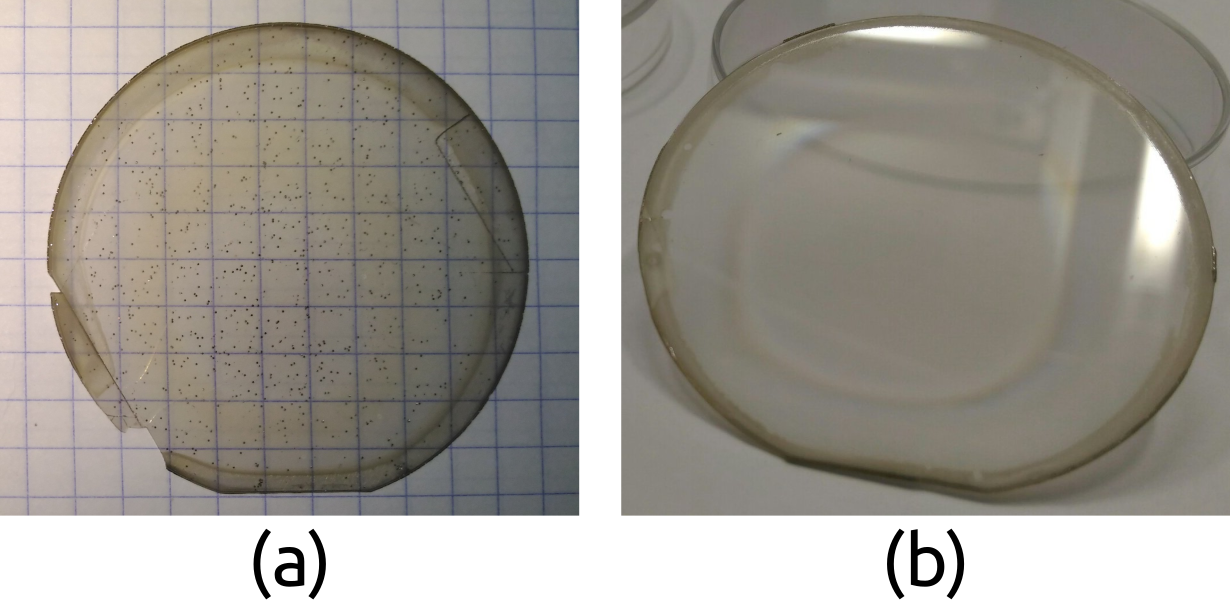 Figure 1
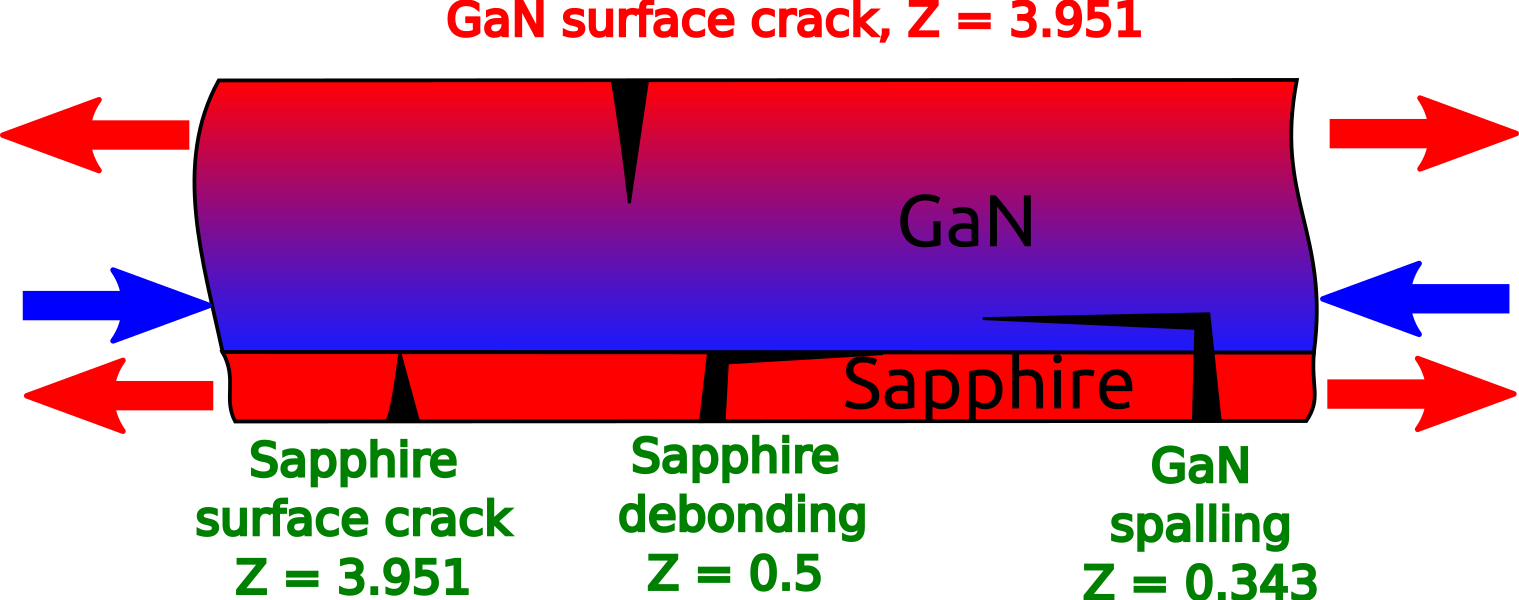 Figure 2
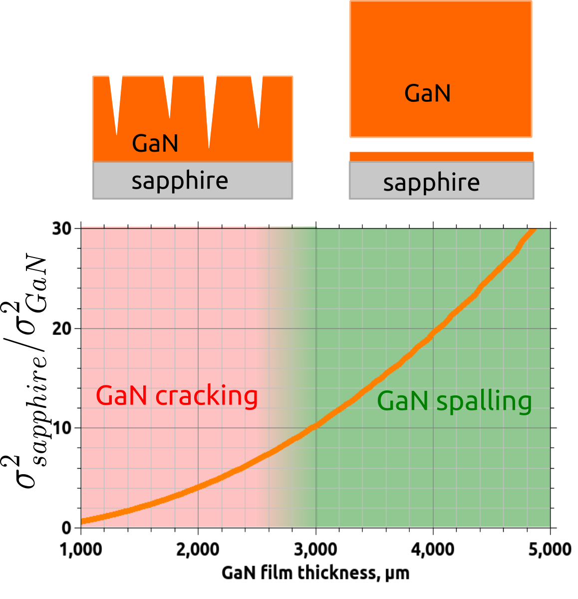 Figure 3
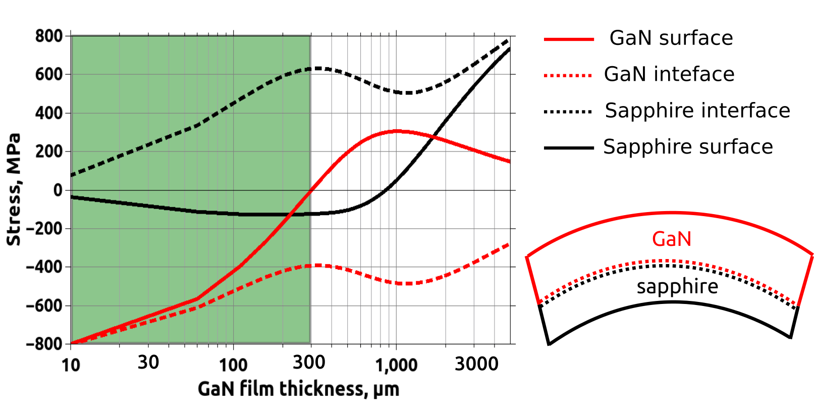 Figure 4
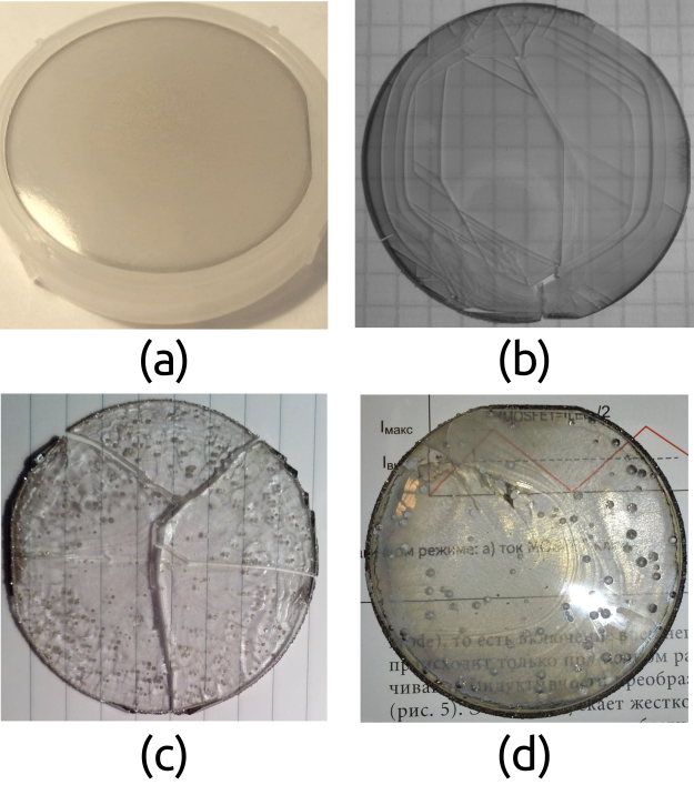 Figure 5
Peer Reviews
No public reviews on file for this paper yet. If you reviewed it on a platform where reviews are public (OpenReview, ICLR, NeurIPS, ICML), you can paste yours below so the community can read it here.
Videos
No videos yet. Explain this paper in a talk, walkthrough, or lecture? Add one.
Thick GaN film stress-induced self-separation
Vladislav Voronenkov1
Andrey Leonidov2
Yuri Lelikov1
Andrey Zubrilov1
Yuri Shreter1
1 Ioffe Physical-Technical Institute, St. Petersburg, Russia
2 Peter the Great St. Petersburg Polytechnic University, St. Petersburg, Russia
Abstract
Cracking of thick GaN films on sapphire substrates during the cooling down after the growth was studied. The cracking was suppressed by increasing the film-to-substrate thickness ratio and by using an intermediate carbon buffer layer, that reduced the binding energy between the GaN film and the substrate. Wafer-scale self-separation of thick GaN films has been demonstrated.
I Introduction
Gallium nitride substrate is the basis of modern high current density devices: high-voltage diodes and transistors ohta2015pndiode13GW ; palacios2016vfet , light emitting diodes nakamura2015bulkLED , vertical cavity surface emitting lasers sony2016vcsel , superluminescent light emitting diodes feltin2009SLED , high electron mobility transistors kuball2012HEMTthermo ; kuball2012HEMT-nonarrenius ; ammono2014HEMT . The main method for the production of GaN substrates today is the hydride vapor phase epitaxy growth of bulk GaN film on a foreign substrate, usually sapphire. An important step of the technological process with this approach is the separation of the bulk GaN film from the foreign substrate after growth, which is usually done by removing the substrate with laser lift-off kelly1999hvpe-liftoff ; gogova2005llo , or by stress-driven self-separation along the weakened interface between the substrate and the film USUI-VAS-2003 ; HENNIG2008911-WSiN-ELOG or parallel to the interface Natural-Stress-Moustakas2007 ; ASHRAF20102-FS-GaN-selfseparation ; fujito2009-5mm ; YAMANE20121 . Cracking of the GaN film during the cooling down and during the self-separation process is a significant problem, reducing the yield of the process. Crack-free cooling of GaN films on a sapphire substrate was obtained for films with a thickness of up to 300 m, such films were then separated from the substrate using the laser lift-off method kelly1999hvpe-liftoff ; gogova2005llo . Successful wafer-scale stress-induced self-separation has been reported for GaN films with a thickness of millimeters fujito2009-5mm , while cracking of GaN films with lower thickness was observed Natural-Stress-Moustakas2007 unless special intermediate layers weakening the bonding between the film and the substrate are used USUI-VAS-2003 ; HENNIG2008911-WSiN-ELOG . In this work, the processes of self-separation and cracking of thick GaN films on sapphire substrates are investigated, and the parameters for the reproducible crack-free self-separation are determined.
II Experimental
II.1 Self-separation of GaN films on sapphire substrates
A set of more than 100 GaN films with a thickness from 100 to 5000 were grown on c-plane sapphire substrates with a thickness of 430 and a diameter of 52 (2 inch). The two-stage growth process was used to grow crack-free films with smooth surface VVVvoronenkov2013two . No special substrate surface treatment to weaken the bonding between the substrate and the GaN film was employed.
The following typical failure modes were observed, depending on the thickness of the GaN film:
- •
No self-separation occurred and no cracks were generated inside GaN film and inside the sapphire substrate for GaN films thickness less than 300 m (fig. 1a).
- •
Films with a thickness from 300 m to 2500 m cracked into multiple pieces (fig. 1b,c). Self-separation of the GaN film from the substrate was observed in a plane located inside the GaN film parallel to the interface. The separated area of the film increased with increasing film thickness – from the absence of separation for a 400-m thick film to complete separation for a 2000-m thick film.
- •
Films with a thickness higher than 2800 m self-separated as a single piece without cracking (fig. 1d). The separation plane was located inside the GaN film at a distance of 200-400 m from the interface.
II.2 Self-separation of GaN film on a sapphire substrate with a carbon buffer
layer
GaN film with a thickness of 365 m was grown epitaxially on a sapphire substrate with a thickness of 430 m using a carbon buffer layer CARBON-Phil-2016 . The carbon buffer layer was deposited by methane thermal decomposition process from a CH4/H2 mixture BECKER1998-ch4-h2 at a deposition temperature of 1020 *∘*C, a process pressure of 105 kPa and a CH4 partial pressure of 1.3 kPa. The GaN film self-separated as a single piece during cooling down after the growth (fig. 2). Self-separation occurred along the interface of the GaN film and the substrate.
III Discussion
III.1 Crack types
The following types of cracks were observed in thick GaN films, grown on sapphire substrates, after cooling down: surface and channeling cracking of sapphire and GaN, sapphire debonding along the interface and sapphire debonding by spalling (fig. 3). In case of spalling the crack propagates inside the GaN film parallel to the interface at a depth at which the in-plane shear stress intensity factor SUO1989spalling . The steady-state spalling depth depends on the elastic mismatch between GaN and sapphire, and on the thicknesses of the GaN film and the sapphire substrate SUO1989spalling .
Sapphire debonding leads to self-separation of GaN film and is desirable or at least permissible. Surface crack formation in the GaN film results in cracking of the film into several parts during cooling down or during further processing and is completely unacceptable.
To determine crack-free conditions for cooling and separation, the stress distribution in the GaN film and the sapphire substrate and the driving forces for crack formation were calculated.
III.2 Stress distribution
The deformation and distribution of stresses in a sapphire substrate of radius and thickness , with a GaN film of thickness were calculated by the minimization of the total strain energy, assuming that the solution of the problem has radial symmetry. Elastic properties of sapphire and GaN were assumed isotropic with the Young’s moduli of GaN and sapphire GPa and GPa and the Poisson’s ratios and deger1998gan-elastic ; wagner2002properties ; watchman1961sapphire-young ; engel1960sapphire-poisson .
The built-in strain was calculated taking into account the temperature dependence of the thermal expansion coefficients:
[TABLE]
where is the growth temperature, is the room temperature and are the thermal expansion coefficients of GaN and sapphire reeber2000lattice ; krzhyzhanovsky1973thermophysical-oxydes .
The components of the displacement vector in the interface plane were taken as trial functions:
[TABLE]
[TABLE]
where – radial displacement component, – vertical displacement component, – variation parameters. Kirchhoff’s hypothesis is used to approximate the displacement field:
[TABLE]
[TABLE]
Nonlinear terms were taken into account when calculating the dependence of the strain tensors on the displacement vector in cylindrical coordinates:
[TABLE]
[TABLE]
[TABLE]
[TABLE]
The stress tensor components and the specific elastic energy:
[TABLE]
[TABLE]
[TABLE]
[TABLE]
[TABLE]
The total strain energy is obtained by integrating over volume:
[TABLE]
The minimum potential energy F is found from the solution of a system of nonlinear equations:
[TABLE]
Analytical expressions for the system of nonlinear equations 16 were obtained using the computer algebra system maxima . The numerical solution of the equation system 16 was obtained using the Powell’s method powell1964efficient . The results are shown in fig. 4.
III.3 Driving force for cracking
When the sapphire substrate thickness is m and the thickness of the GaN film is less than m, the stress in the GaN film and on the sapphire substrate surface is compressive (fig. 4), and the formation of surface and channeling cracks in the GaN film and in the sapphire substrate is energetically unfavorable.
When the GaN film thickness is higher than m, several competing cracking processes shown in fig. 3 take place. What type of crack will arise first during the cooling process, depends on the distribution of the stress in the substrate-film structure. The driving force for cracking is the elastic strain energy
[TABLE]
that is released during the crack formation. A crack of a certain type can propagate if the energy release rate for this type of crack exceeds the surface energy of the formed crack :
[TABLE]
where is a dimensionless parameter depending on the crack geometry, – stress in the film, – Young’s modulus of the film, – crack length HUTCHINSON1991MMCLM . Sapphire substrate cracking and separation by debonding and spalling is determined by tensile stress in the substrate , cracking of GaN film is determined by tensile stress on the GaN film surface . The ratio of energy release rates for spalling and for GaN cracking is proportional to . With an increase in this ratio, it can be expected that the spalling crack will be initiated and complete self-separation of the substrate will occur before the stress on the surface of the GaN film exceeds the fracture resistance. The dependence of the stress ratio on the thickness of the GaN film at a sapphire substrate thickness of 430 m is shown in fig. 5. The stress ratio increases with increasing the GaN film thickness. Cracking of GaN films observed at 2500 m corresponds to . Reproducible separation without cracking observed at 2800 m corresponds to .
Besides increasing the ratio by increasing the GaN film thickness, another way to promote self-separation is to reduce the binding energy between the film and the substrate. The surface energy of spalling crack in GaN is 6.7 J/m2Li2015-GaN-surface-energy , the use of the carbon buffer layer reduces the binding energy to 0.27 J/m2Liu2012-graphite-binding , which allowed to obtain wafer-scale self-separation of the GaN film with thickness of 365 (fig. 2).
IV Conclusion
The thermal stress arising in a thick GaN film on a sapphire substrate during the cooling down after growth is the driving force of the GaN film cracking and the GaN self-separation. Crack-free freestanding GaN film can be obtained in several ways:
- •
Growing GaN film with thickness m. In this case, the stresses on the free surfaces of the GaN film and the sapphire substrate are compressive and the surface cracking process is energetically unfavorable. The laser lift-off method can be used to separate the GaN film from the sapphire substrate.
- •
Growing GaN film with thickness m. In this case the stress in the sapphire substrate is significantly higher than the stress in the GaN film, and complete separation of the substrate by spalling occurs before the stress in the GaN film exceeds the fracture resistance.
- •
Growing GaN films on an intermediate layer with a low binding energy. For example, a crack-free self-separation of a 365-m thick GaN film was demonstrated using a carbon buffer layer.
The reference list from the paper itself. Each links out to its DOI / PubMed record.
- 1(1) H. Ohta, N. Kaneda, F. Horikiri, Y. Narita, T. Yoshida, T. Mishima, and T. Nakamura, “Vertical Ga N p-n Junction Diodes With High Breakdown Voltages Over 4 k V,” IEEE Electron Device Letters , vol. 36, no. 11, pp. 1180–1182, Nov 2015. [Online]. Available: https://doi.org/10.1109/LED.2015.2478907 · doi ↗
- 2(2) M. Sun, Y. Zhang, X. Gao, and T. Palacios, “High-Performance Ga N Vertical Fin Power Transistors on Bulk Ga N Substrates,” IEEE Electron Device Letters , vol. 38, no. 4, pp. 509–512, April 2017. [Online]. Available: https://doi.org/10.1109/LED.2017.2670925 · doi ↗
- 3(3) C. A. Hurni, A. David, M. J. Cich, R. I. Aldaz, B. Ellis, K. Huang, A. Tyagi, R. A. De Lille, M. D. Craven, F. M. Steranka, and M. R. Krames, “Bulk Ga N flip-chip violet light-emitting diodes with optimized efficiency for high-power operation,” Applied Physics Letters , vol. 106, no. 3, p. 031101, 2015. [Online]. Available: https://doi.org/10.1063/1.4905873 · doi ↗
- 4(4) T. Hamaguchi, N. Fuutagawa, S. Izumi, M. Murayama, and H. Narui, “Milliwatt-class Ga N-based blue vertical-cavity surface-emitting lasers fabricated by epitaxial lateral overgrowth,” physica status solidi (a) , vol. 213, no. 5, pp. 1170–1176, 2016. [Online]. Available: https://doi.org/10.1002/pssa.201532759 · doi ↗
- 5(5) E. Feltin, A. Castiglia, G. Cosendey, L. Sulmoni, J.-F. Carlin, N. Grandjean, M. Rossetti, J. Dorsaz, V. Laino, M. Duelk, and C. Velez, “Broadband blue superluminescent light-emitting diodes based on Ga N,” Applied Physics Letters , vol. 95, no. 8, p. 081107, 2009. [Online]. Available: https://doi.org/10.1063/1.3202786 · doi ↗
- 6(6) N. Killat, M. Montes, J. W. Pomeroy, T. Paskova, K. R. Evans, J. Leach, X. Li, U. Ozgur, H. Morkoc, K. D. Chabak, A. Crespo, J. K. Gillespie, R. Fitch, M. Kossler, D. E. Walker, M. Trejo, G. D. Via, J. D. Blevins, and M. Kuball, “Thermal Properties of Al Ga N/Ga N HFE Ts on Bulk Ga N Substrates,” IEEE Electron Device Letters , vol. 33, no. 3, pp. 366–368, March 2012. [Online]. Available: https://doi.org/10.1109/LED.2011.2179972 · doi ↗
- 7(7) M. Tapajna, N. Killat, J. Moereke, T. Paskova, K. R. Evans, J. Leach, X. Li, U. Ozgur, H. Morkoc, K. D. Chabak, A. Crespo, J. K. Gillespie, R. Fitch, M. Kossler, D. E. Walker, M. Trejo, G. D. Via, J. D. Blevins, and M. Kuball, “Non-Arrhenius Degradation of Al Ga N/Ga N HEM Ts Grown on Bulk Ga N Substrates,” IEEE Electron Device Letters , vol. 33, no. 8, pp. 1126–1128, Aug 2012. [Online]. Available: https://doi.org/10.1109/LED.2012.2199278 · doi ↗
- 8(8) P. Kruszewski, P. Prystawko, I. Kasalynas, A. Nowakowska-Siwinska, M. Krysko, J. Plesiewicz, J. Smalc-Koziorowska, R. Dwilinski, M. Zajac, R. Kucharski, and M. Leszczynski, “Al Ga N/Ga N HEMT structures on ammono bulk Ga N substrate,” Semiconductor Science and Technology , vol. 29, no. 7, p. 075004, 2014. [Online]. Available: https://doi.org/10.1088/0268-1242/29/7/075004 · doi ↗