A nonlinear, geometric Hall effect without magnetic field
Nicholas B. Schade, David I. Schuster, Sidney R. Nagel

TL;DR
This paper demonstrates a nonlinear, geometric Hall effect in curved graphene wires that produces transverse voltages reflecting charge-carrier properties without magnetic fields, revealing new ways to characterize current flow.
Contribution
It introduces a magnetic-field-free, geometry-induced Hall effect in curved conductors, providing a novel method to determine charge-carrier sign and density.
Findings
Curved graphene wires exhibit transverse potentials consistent with doping.
Straight wires show random transverse potential fluctuations.
The effect enables sensitive characterization of inhomogeneous current flow.
Abstract
The classical Hall effect, the traditional means of determining charge-carrier sign and density in a conductor, requires a magnetic field to produce transverse voltages across a current-carrying wire. We show that along curved paths -- any magnetic field -- geometry alone can produce nonlinear transverse potentials that reflect the charge-carrier sign and density. We demonstrate this effect in curved graphene wires where the transverse potentials are consistent with the doping and change polarity as we switch the carrier sign. In straight wires, we measure transverse potential fluctuations with random polarity demonstrating that the current follows a complex, tortuous path. This geometrically-induced potential offers a sensitive characterization of inhomogeneous current flow in thin films.
Click any figure to enlarge with its caption.
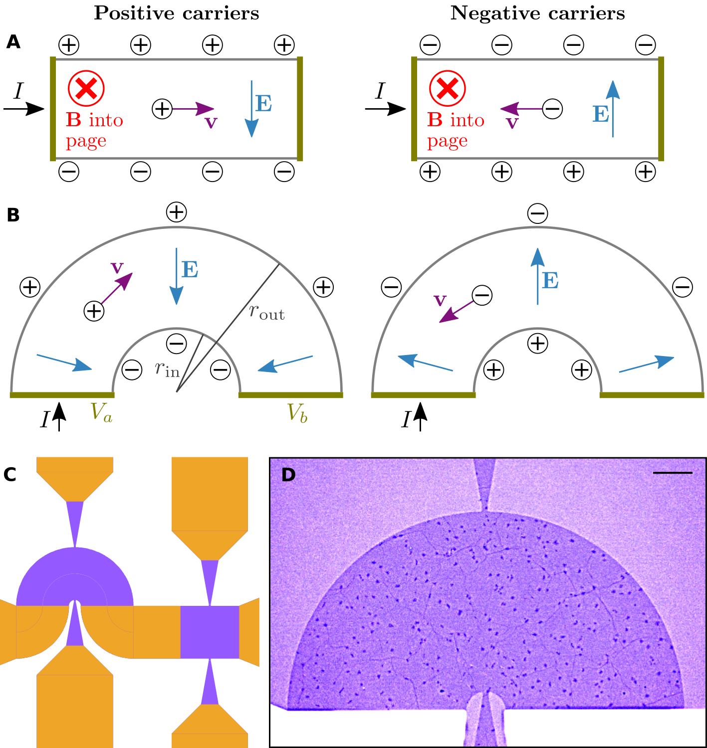 Figure 1
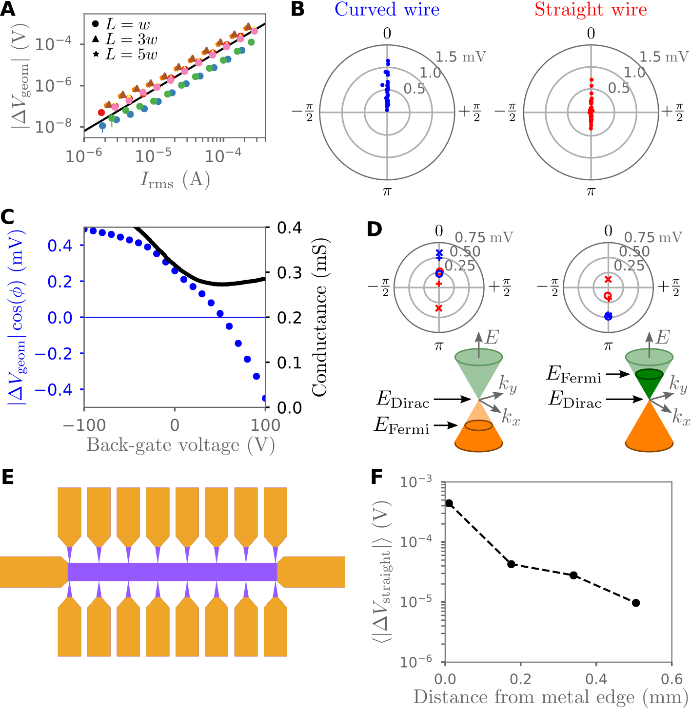 Figure 2
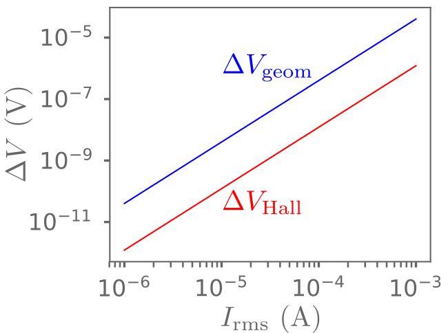 Figure 3
Peer Reviews
No public reviews on file for this paper yet. If you reviewed it on a platform where reviews are public (OpenReview, ICLR, NeurIPS, ICML), you can paste yours below so the community can read it here.
Videos
No videos yet. Explain this paper in a talk, walkthrough, or lecture? Add one.
A nonlinear, geometric Hall effect without magnetic field
Nicholas B. Schade,1∗, David I. Schuster,2 and Sidney R. Nagel1
1Department of Physics and the James Franck and Enrico Fermi Institutes,
University of Chicago, Chicago, IL 60637, USA
2Department of Physics and the James Franck Institute,
University of Chicago, Chicago, IL 60637, USA
∗To whom correspondence should be addressed; E-mail: [email protected]
Abstract
The classical Hall effect, the traditional means of determining charge-carrier sign and density in a conductor, requires a magnetic field to produce transverse voltages across a current-carrying wire. We show that along curved paths – without any magnetic field – geometry alone can produce nonlinear transverse potentials that reflect the charge-carrier sign and density. We demonstrate this effect in curved graphene wires where the transverse potentials are consistent with the doping and change polarity as we switch the carrier sign. In straight wires, we measure transverse potential fluctuations with random polarity demonstrating that the current follows a complex, tortuous path. This geometrically-induced potential offers a sensitive characterization of inhomogeneous current flow in thin films.
In 1879, Edwin Hall discovered that a transverse potential appears across a current-carrying wire placed in a magnetic field [1]. Physics instructors traditionally teach the Hall effect when the magnetic field is first presented in introductory electricity and magnetism as the way to distinguish the sign of the charge carriers in a conductor [2]. Indeed, the Hall effect is an efficient way to disentangle the role of electron and hole conduction in semiconductors [3] and is commonly used to measure the magnitude of magnetic fields [4]. Here we present a different mechanism using geometry alone, without a magnetic field, to produce a transverse voltage that also reflects the sign and density of the charge carriers. A current traveling through a curved wire must undergo centripetal acceleration to follow the curve. This acceleration occurs due to electric fields from charges distributed along the wire edges; the direction of the field must change with the sign of the carriers. No magnetic field is necessary.
The transverse voltage that we predict and measure is quadratic in the current. It is therefore distinct from many linear Hall effects such as the spin- [5], valley- [6], and anomalous- [7] Hall effects. However, the geometric effect we describe should be contrasted with predictions [8] and recent measurements of a nonlinear Hall effect in nonmagnetic bilayer materials such as WTe2 [9].
By 1850, Kirchhoff realized that surface charge distributions are necessary simply to confine a current inside a wire [10]. Subsequently, the role of surface charges has been investigated theoretically [11, 12, 13] and experimentally using single-electron transistors [14, 15]. The effect we describe is also related to how currents are confined within wires. Our experiments show that the effect can be used for sensitively probing non-homogeneous current flow in thin films as well as systems where magnetic fields do not occur such as the bulk of a superconductor. While the effect is small, it is measurable even in bulk conductors. Using graphene wires to optimize the signal, we measure transverse potentials 0.5 mV.
In the conventional Hall effect, when an electric current of charge carriers passes through an applied magnetic field , the carriers experience a magnetic Lorentz force . Charge accumulates at the wire edges, as illustrated in Fig. 1A, until the electric field caused by these charges cancels to create a transverse potential difference:
[TABLE]
Here is the charge-carrier density and the wire thickness along the direction of . A measurement of determines and the sign of the charge carriers.
To show that magnetism is not necessary for producing transverse voltages sensitive to and the sign of , we take advantage of surface charge distributions that are a result of geometry – curvature in the path of the current – rather than magnetic forces. The surface charges create a transverse component of the electric field and exert a force on the current such that it follows the wire. For a wire in the shape of a circular arc, the transverse electric force must point radially towards the circle center to accelerate the carriers centripetally; this mandates that the direction of the radial electric field (and thus the potential difference between the wire edges) depends on the sign of the current carriers, as illustrated in Fig. 1B. The polarity of this potential, analogous to the polarity of a Hall potential, reveals the sign of the carriers.
Calculating this potential is straightforward. We assume the wire is a semicircular annulus with inner radius and outer radius ; the wire has a rectangular cross-section of width and thickness . We force the radial edges of the half annulus to be equipotentials, as illustrated in Fig. 1B, with potential difference . Due to azimuthal symmetry, the charges on average follow semicircular trajectories. We assume that the conductivity and carrier density are uniform and that all charge carriers have the same mass and charge .
Unless the wire is a superconductor, the current density, , is equal to the longitudinal (azimuthal) component of the electric field, , times the conductivity: . The transverse (i.e., radial) component, , provides the force necessary for the carriers to follow circular paths.
The local velocity of the carriers is proportional to the current density: and the force for keeping these particles in a circular orbit of radius is . The radial electric field is thus
[TABLE]
where is the electrostatic potential. This can be integrated across the width of the wire, , to find :
[TABLE]
The terms in square brackets depend only on the wire geometry; the approximations in Eq. 4 are valid in the narrow-wire limit, , with being the average current density. As in the Hall effect, the potential is an odd power of the charge , which means that the sign of can be determined.
There are two significant differences between this transverse potential and the Hall effect. The first is that the mass of the carriers, , enters into the expression for the potential difference. Whether should be the bare or the effective mass of the carriers is an important open theoretical question. The second difference is that is quadratic, rather than linear, in the current, .
To maximize the signal , we need high current (or current density ) and low carrier density . It is advantageous to use a conductor whose charge-carrier sign and density can be modulated in order to check whether the signal and carriers change sign concurrently. Monolayer graphene satisfies these conditions [16].
Our circuit, illustrated in Fig. 1C, consists of a curved graphene wire with measurement leads on either side, and a straight graphene wire as a control. We use graphene grown by chemical vapor deposition and transferred by the manufacturer (Graphenea) to a doped silicon wafer with a 300 nm oxide gap. We use photolithography, electron-beam evaporation, and plasma etching to pattern the graphene and to place Ti/Au contacts on it, as shown in Fig. 1D. (See SI for detailed nanofabrication procedure.) We control the sign and density of the carriers in the graphene by applying a back-gate voltage to the silicon. As initially fabricated, the samples are highly doped; we current-anneal [17] them to cross the Dirac point at 100 V.
The fact that the signal is quadratic in the current may be exploited to remove several potential sources of measurement error. The dependence means that an AC current at frequency produces a transverse potential at frequency . We use a lock-in amplifier to measure the potential at while filtering out potentials at . A Hall potential due to a DC magnetic field, such as that of the earth, will appear at and thus can be safely ignored. The potential drop due to the longitudinal electric field component within the wire, , likewise occurs at , so we need not worry about imperfect alignment of transverse measurement leads. By checking that is proportional to , we ensure that any harmonics in the current do not contribute to the signal. Fluctuations in the conductor’s resistivity due to Joule heating give rise to longitudinal oscillations in the potential that occur at and higher harmonics, but not at . (See SI for details.)
Two extraneous sources of a signal are due to (i) the Hall voltage from a current-induced magnetic field and (ii) the Seebeck effect. In the SI we describe how we have minimized their contribution so that they do not affect our results.
We have measured the potential difference, , across the curved wires in our samples. In all the samples, without any current-annealing and at , is positive, corresponding to positive charge carriers. This is what is expected in graphene on a SiO2 substrate [16, 15, 18]. We fit the measured transverse potentials to a power of the current amplitude, , and we find . This confirms that the measured potential rises quadratically with the current, as shown in Fig. 2A. There is significant scatter in the signal magnitude between samples as shown in Fig. 2B. For a driving voltage 1.00 V, the current is A and the average magnitude of the signal is 0.46 mV. Using Eq. 3 and averaging over the samples, we measure kg m4 C*-3*.
After current annealing, we can apply a back-gate voltage to the sample and move the Fermi level to the other side of the Dirac point where the charge of the carriers has the opposite sign. We find that changes sign at a back-gate voltage close to that of the conductance minimum, as shown in Fig. 2C. This confirms that this measurement determines the sign of the charge carriers using only geometry. (This behavior shows hysteresis with the direction of the sweep, as is typical of electrical properties of graphene [18].) Rather than showing a singularity, passes smoothly through zero near the Dirac point. This is consistent with prior observations that in graphene samples near the Dirac point, inhomogeneities and defects make the graphene behave as a random assortment of electron and hole puddles rather than as a uniform material with [15, 19, 20, 21].
Because our samples are thin, the current is small even though the current density is very large. Therefore, the magnitude of the Hall-effect contribution from a current-induced magnetic field should be (see Fig. S1) at least 20 times smaller than the signal we observe and the prediction of Eq. 3. We have also checked (see SI) that is not due to the Seebeck effect by varying the length of the graphene voltage-measuring leads.
The sign of the potential difference, , between the two sides of the straight wire, is not picked out by the curvature of the wire. However, we still find a signal whose phase is either or , as shown in Fig. 2B. The average signal over many samples , but in a single sample, the magnitude of the signal in the straight section can be comparable to, but usually smaller than, that in the curved section. We find . As we sweep in a sample that has been current-annealed, changes sign (just as does ), as shown in Fig. 2D.
We have measured from a long straight wire with 8 pairs of electrodes across it, illustrated in Fig. 2E. We average over four long-wire samples and find that the magnitude of falls off with , the distance from where the graphene makes contact with the metal source and drain as shown in Fig. 2F. The potential drops by nearly two orders of magnitude from near the leads, where 10 m, to the center, where 500 m.
It is unexpected that there is a significant signal across a straight section of wire. The sign of this voltage varies from place to place along the wire and in different samples and its magnitude is smaller than, but comparable to, that in the curved section. We conclude that the reason for this behavior is that the current paths are not homogeneous. The signal observed in the straight sections is thus due to the current taking a meandering path along the wire.
To rationalize the decrease of from the ends of the wire, we assume that the current is injected from the Ti/Au leads into the graphene at localized points; the current then fans out as it moves down the wire. This is consistent with studies showing that metal contacts introduce inhomogeneous doping [20], and that contact may be poor due to surface impurities on the graphene [15, 22]. Photocurrent mapping of graphene transistors has revealed irregular electrostatic potential landscapes, including at the metal contacts and along the edges [19]. As the current flows down the wire, it expands to fill more of the wire’s width. Because the signal is quadratic in the current density, for fixed total current, the smaller the width, the larger will be the signal.
This interpretation also offers an explanation for the large measured magnitude of . If the mass in Eq. 3 is taken to be the bare mass of the electron with charge , our data suggest a carrier density cm*-2*, which is a tenth the value expected for our doping level [16]. However, if the current paths are not given by the wire width, , but rather by the heterogeneity of the current path, then we can account for the observed large value of by using a smaller width in Eq. 3.
There is considerable evidence that currents in thin metal films [23, 24] and in two-dimensional conductors such as graphene are not uniform throughout the wires. In graphene this has been ascribed to scattering at grain boundaries [25], as well as to charge puddles [15, 21] and local strains [26, 27]. The measurement of a transverse signal, , is an elegant probe of the tortuous current path.
We have demonstrated a transverse voltage across a current-carrying wire due to geometry alone. In the classical Hall effect, a magnetic field curves the paths of charge carriers inside a straight wire so that charges accumulate on the wire edges transverse to the current. In the geometric analog, we do not bend the paths of the carriers but instead bend the conductor itself to create a purely geometric effect. The observed signal is consistent with a prediction from elementary mechanics and electrodynamics.
We observe signals even in straight wires. Although the wires themselves are straight, the internal current paths are not. Just as for curved wires, charge distributions are necessary to confine currents to any heterogeneous path. The nonlinear transverse voltage offers a novel technique for studying such heterogeneities.
Recent work [9] has found a nonlinear Hall effect due to an induced Berry curvature [28] in bilayer conductors. Such an effect is not expected to occur in a single-layer material such as graphene and is not predicted to depend on the wire curvature. Our purely geometric effect can contribute to the signals found in those experiments and in turn those effects, if present, could masquerade as a geometric effect.
Low-temperature quantum Hall effects arise due to time-reversal-symmetry breaking in a magnetic field. In the presence of quantum interactions, the magnetic Hall effect becomes particularly remarkable; it would be interesting to consider if any striking quantum effects can be observed due to geometry alone.
Acknowledgments
We are particularly grateful to Khá-Î Tô who worked on the early stages of this project and to Lujie Huang who gave important advice about nanofabrication with graphene. We thank Jiwoong Park’s group (J. Park, K.-H. Lee, J.-U. Lee, and P. Poddar) as well as G. Koolstra, N. Earnest, S. Chakram, and F. Tang for technical assistance. We thank P.B. Littlewood, C. Panagopoulos, and D.T. Son for helpful discussions. This work was supported by the NSF MRSEC Program DMR-1420709 and NSF DMR-1404841 and used the Pritzker Nanofabrication Facility, supported by NSF ECCS-1542205.
The reference list from the paper itself. Each links out to its DOI / PubMed record.
- 1[1] Edwin H Hall. On a new action of the magnet on electric currents. Am. J. Math. , 2(3):287–292, 1879.
- 2[2] Edward M Purcell. Electricity and Magnetism. Berkeley Physics Course , volume 2. Mc Graw-Hill, New York, 2 edition, 1985.
- 3[3] Georg Busch. Early history of the physics and chemistry of semiconductors-from doubts to fact in a hundred years. Eur. J. Phys. , 10(4):254–264, 1989.
- 4[4] Edward Ramsden. Hall-Effect Sensors: Theory and Applications . Elsevier/Newnes, Amsterdam, 2 edition, 2006.
- 5[5] M. I. Dyakonov and V. I. Perel. Current-induced spin orientation of electrons in semiconductors. Phys. Lett. A , 35(6):459–460, 1971.
- 6[6] Kin Fai Mak, Kathryn L Mc Gill, Jiwoong Park, and Paul L Mc Euen. The valley Hall effect in Mo S 2 transistors. Science , 344(6191):1489–1492, 2014.
- 7[7] Naoto Nagaosa, Jairo Sinova, Shigeki Onoda, A. H. Mac Donald, and N. P. Ong. Anomalous Hall effect. Rev. Mod. Phys. , 82:1539–1592, 2010.
- 8[8] Inti Sodemann and Liang Fu. Quantum nonlinear Hall effect induced by Berry curvature dipole in time-reversal invariant materials. Phys. Rev. Lett. , 115:216806, 2015.