Tilt-induced anomalous thermal transport in normal/superconducting borophane junctions
Moslem Zare

TL;DR
This paper investigates how tilt-induced anisotropy in borophane affects charge and heat transport in normal-superconductor junctions, revealing anomalous thermal conductance behavior and perfect electron-hole conversion at various incident angles.
Contribution
It introduces a detailed analysis of thermal and charge transport in borophane NS junctions, highlighting the impact of Dirac cone tilting on conductance and Andreev reflection processes.
Findings
Unit probability of electron-hole conversion at normal incidence despite Fermi mismatch
Anomalous decrease in thermal conductance with increasing temperature
Tilt of Dirac cones causes unique thermal transport behavior
Abstract
We study charge and heat transport in normal-metal/superconductor (NS) hybrid junction, based on a tilted anisotropic Dirac material. Using the extended Blonder-Tinkham-Klapwijk formalism, the conductance spectra of NS borophane, a two-dimensional Dirac semimetal with two tilted anisotropic Dirac cones in its dispersion, is investigated. Completely different from the usual normal-metal-superconductor junctions, in spite of the large mismatch in Fermi wavevectores of the normal-metal and superconductor sides of the borophane NS junction, the electron-hole conversion happens with unit probability at normal incidences. Furthermore, we demonstrate that in the heavily doped superconducting regime for heavily doped normal borophane, the electron-hole conversion happens with unit probability, approximately at any incident angle. The dependence of the Andreev with Fermi energy and bias voltage,…
Click any figure to enlarge with its caption.
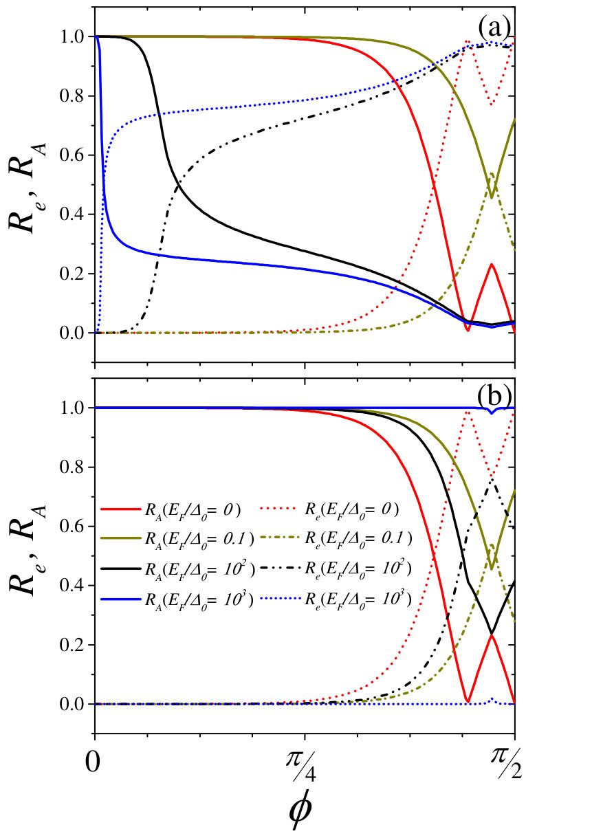 Figure 1
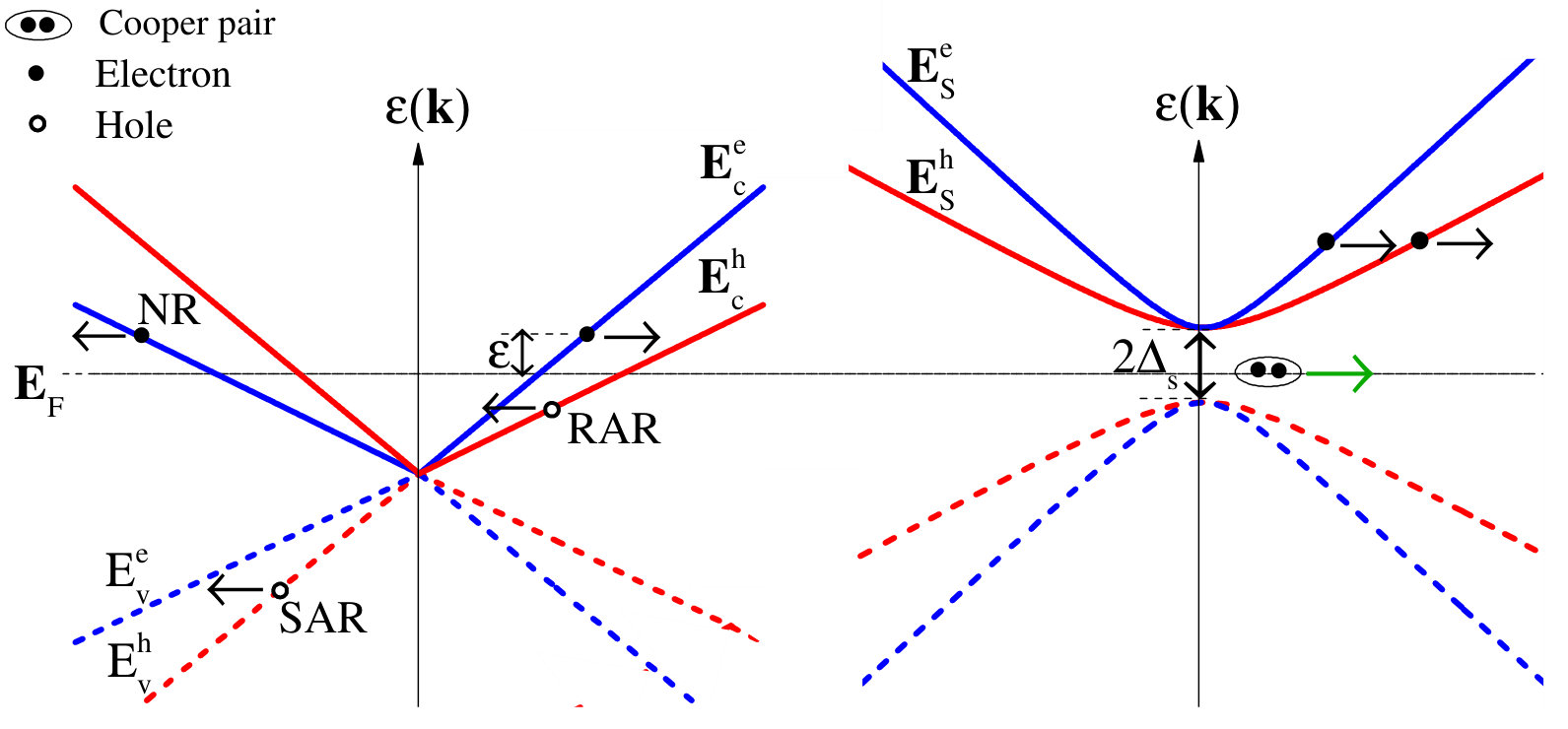 Figure 2
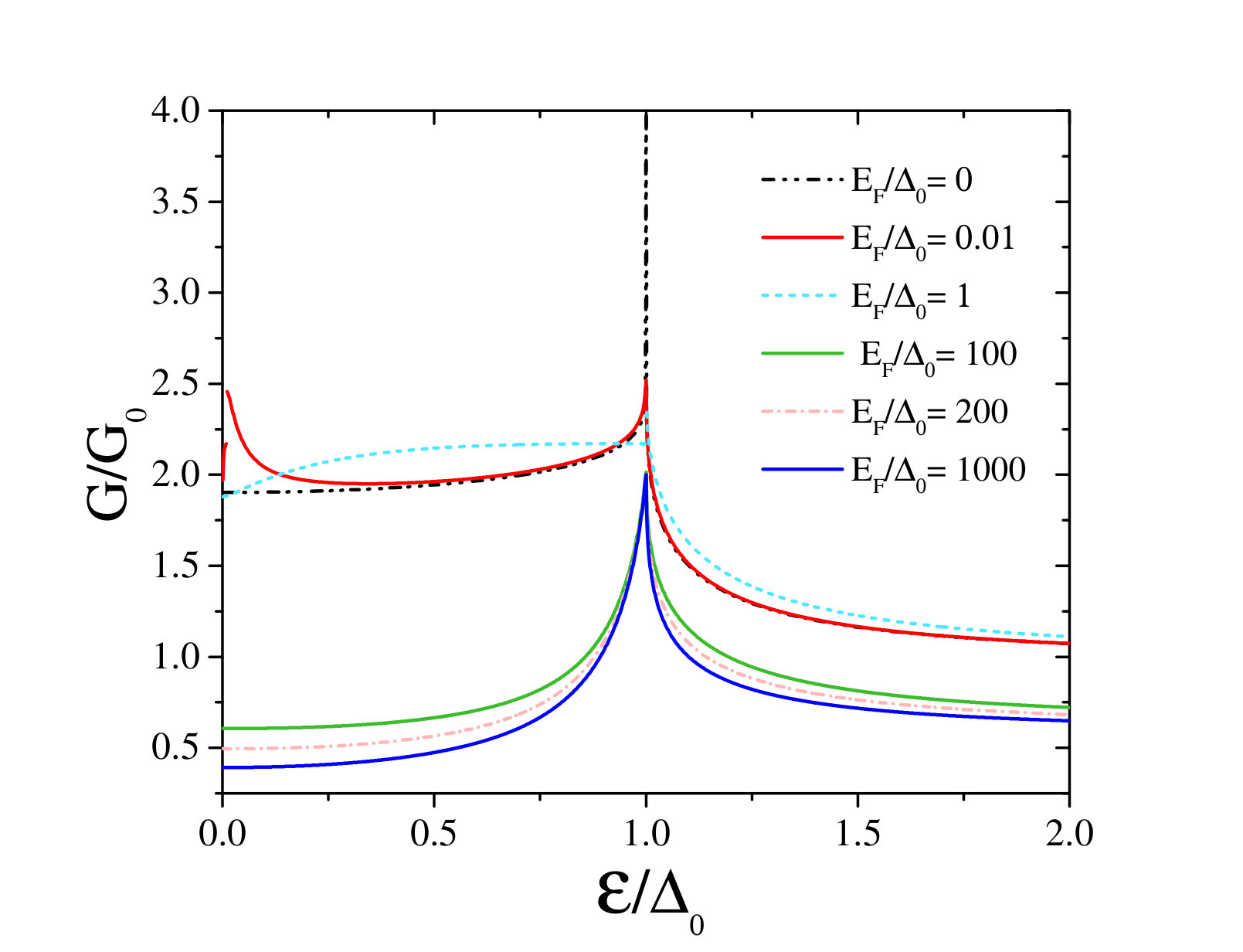 Figure 1
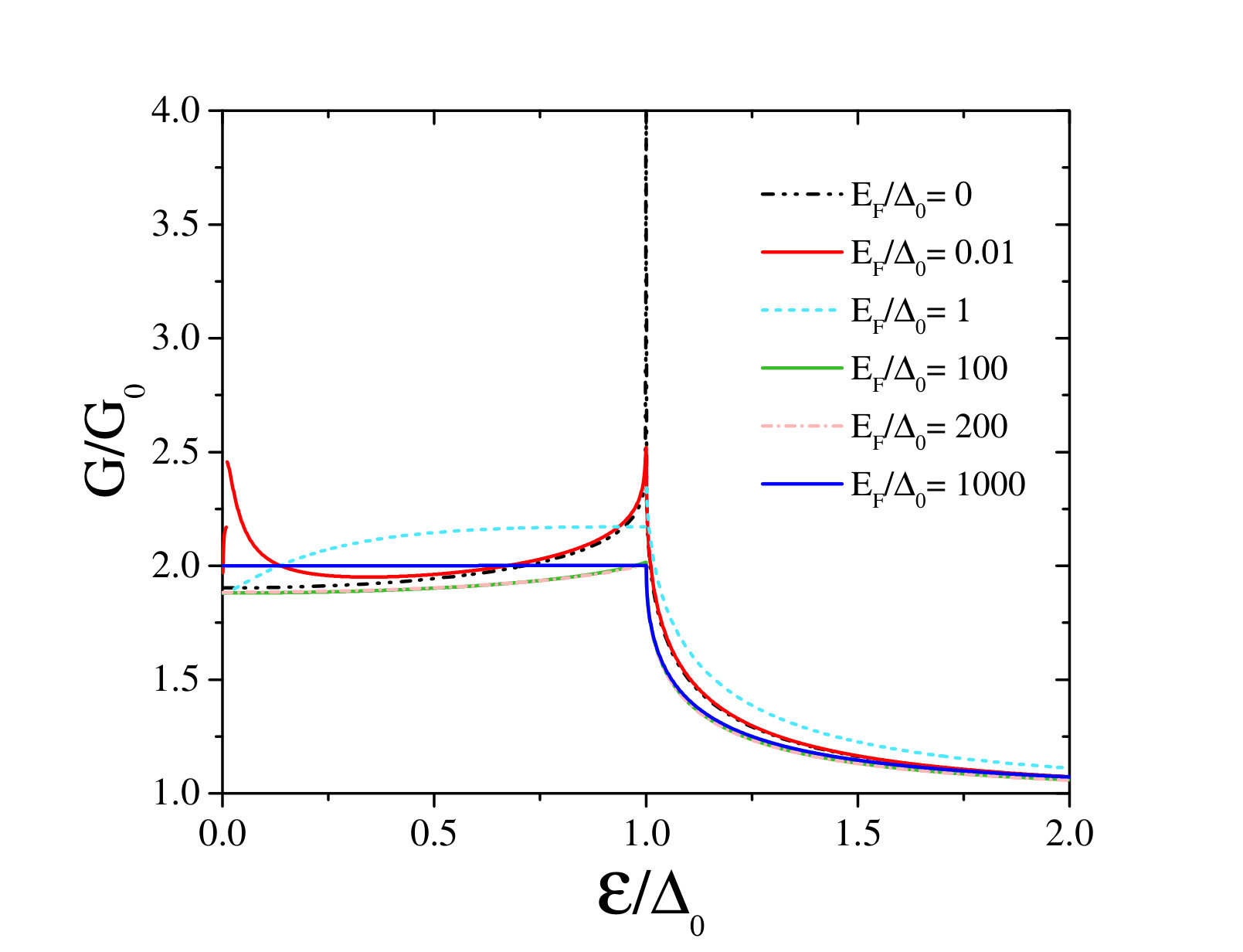 Figure 2
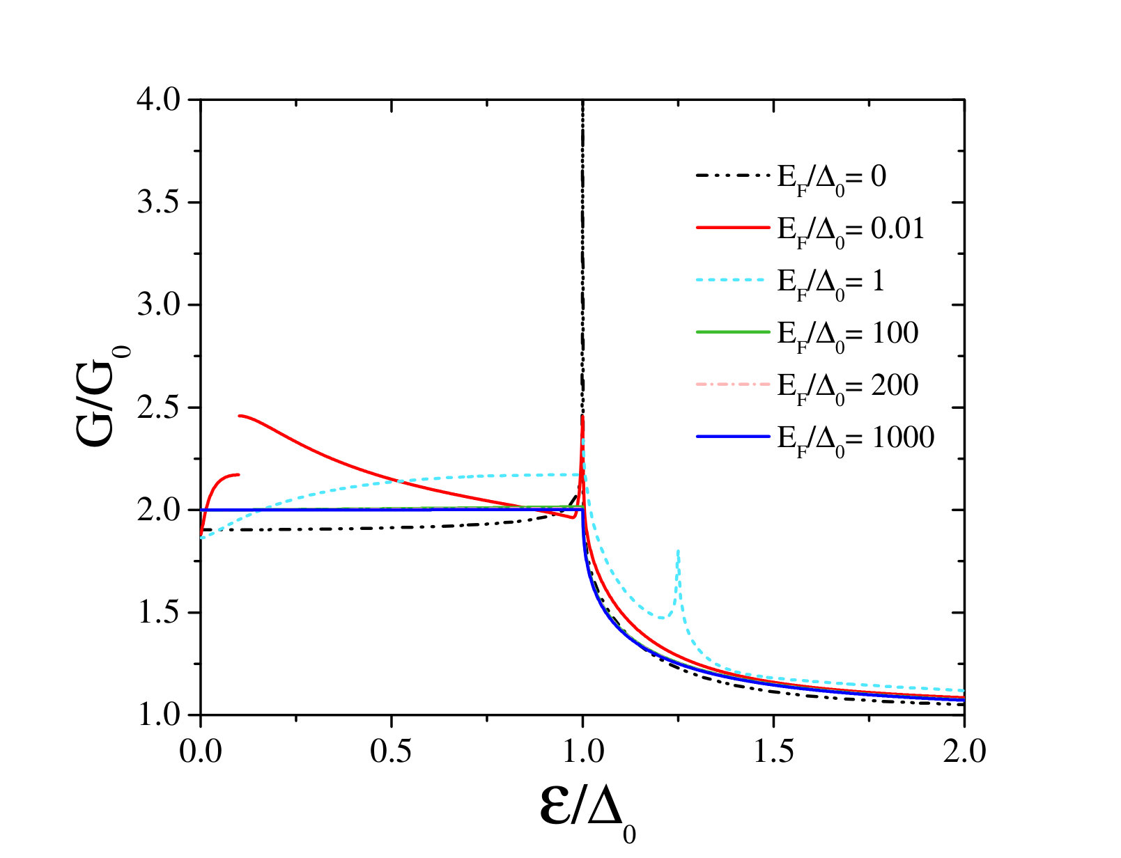 Figure 3
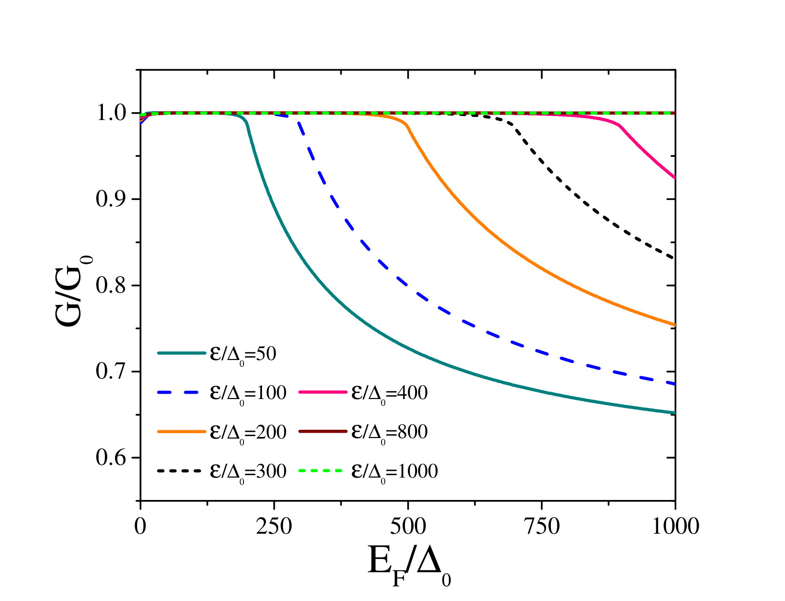 Figure 4
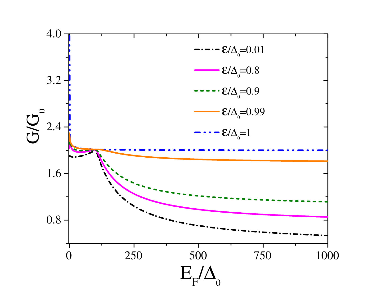 Figure 5
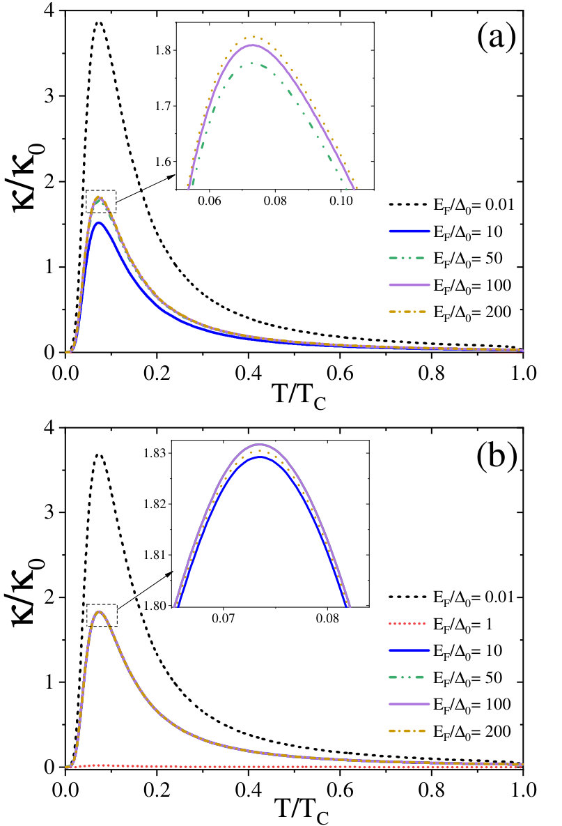 Figure 6
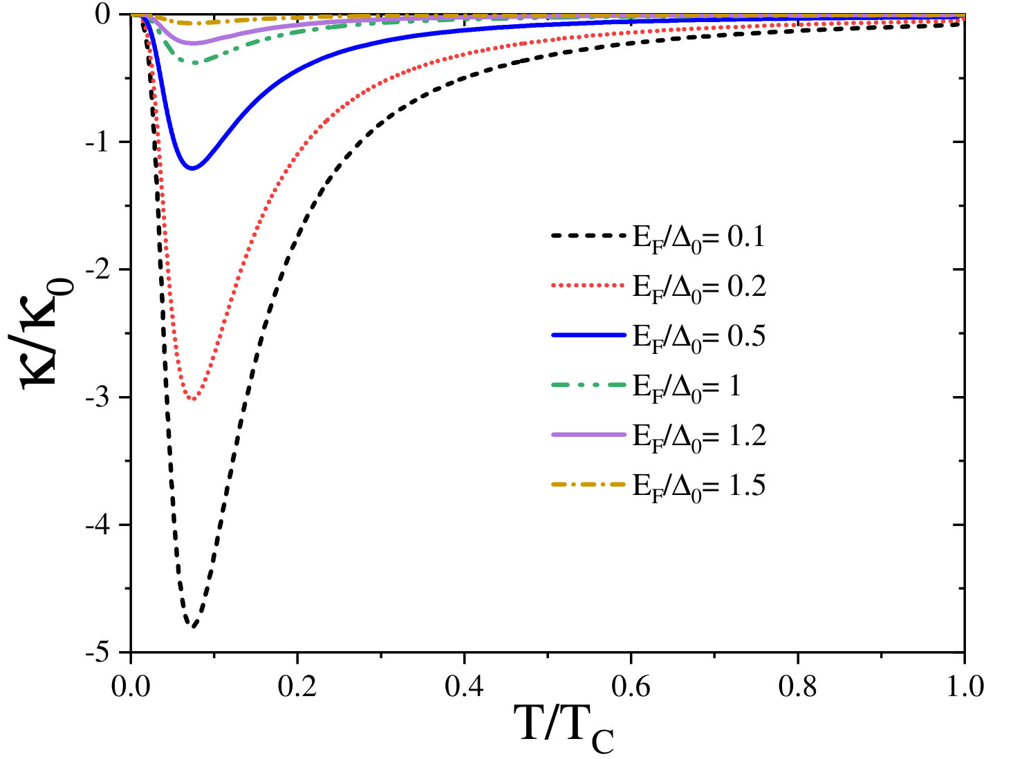 Figure 7
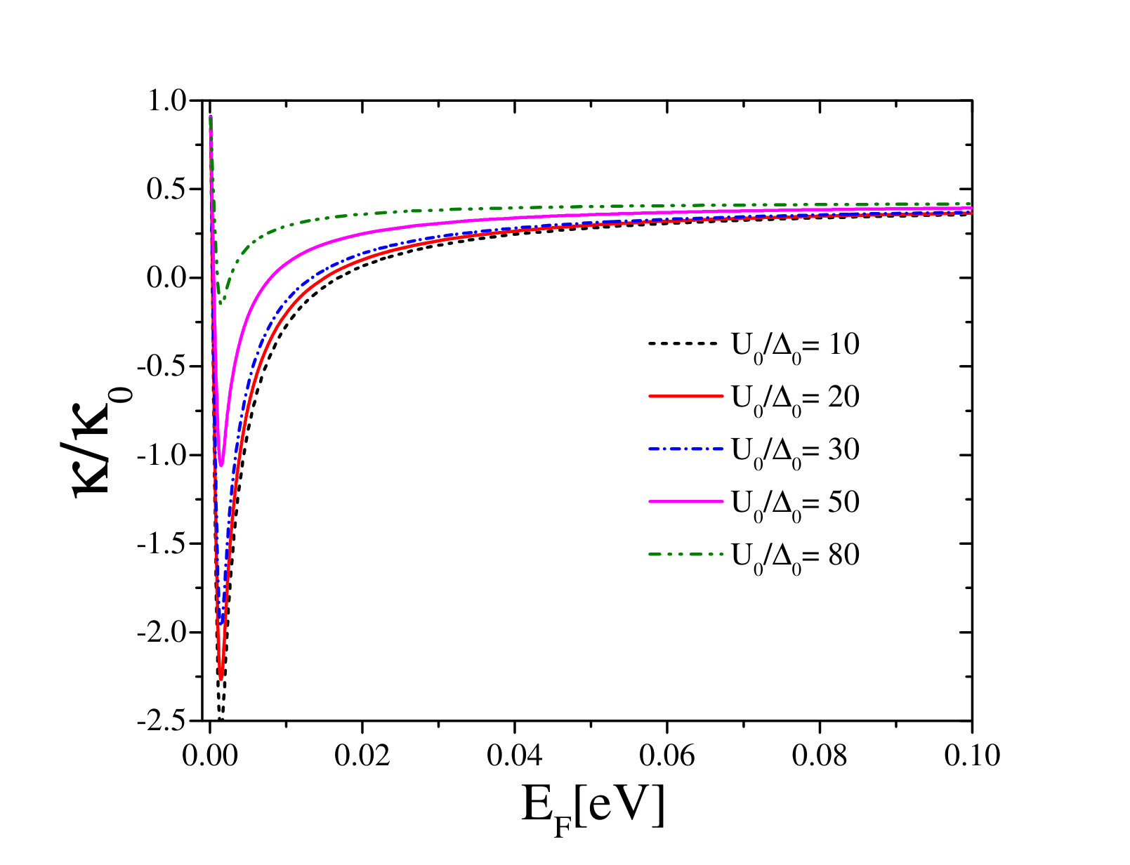 Figure 8
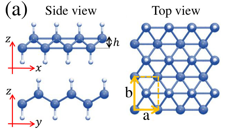 Figure 11
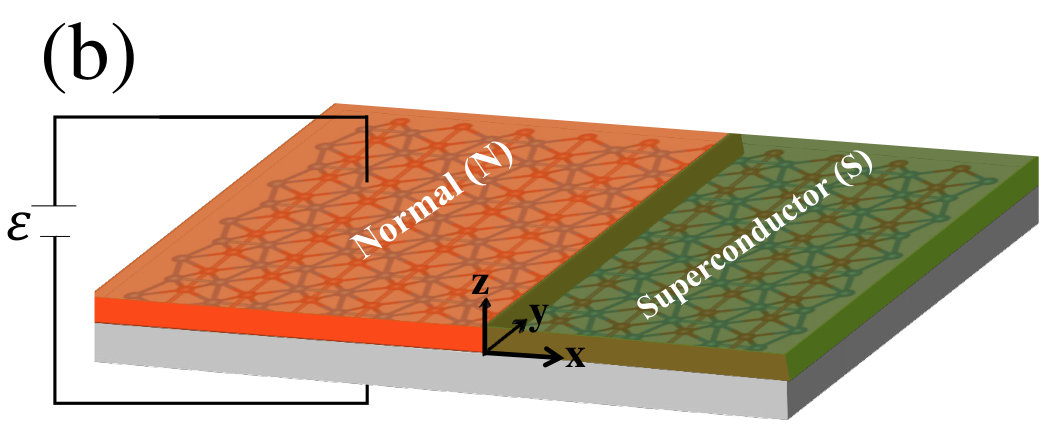 Figure 12
Peer Reviews
No public reviews on file for this paper yet. If you reviewed it on a platform where reviews are public (OpenReview, ICLR, NeurIPS, ICML), you can paste yours below so the community can read it here.
Videos
No videos yet. Explain this paper in a talk, walkthrough, or lecture? Add one.
Taxonomy
TopicsTopological Materials and Phenomena · Quantum, superfluid, helium dynamics · Graphene research and applications
Negative differential thermal conductance in a borophane normal metal-superconductor junction
Moslem Zare
Department of Physics, Yasouj University, 75914-353, Yasouj, Iran
Abstract
We study the charge and heat transport in a normal-metal/superconductor (NS) junction of the tilted anisotropic Dirac cone material borophane, using the extended Blonder-Tinkham-Klapwijk formalism. We numerically find that, in spite of the large mismatch in the Fermi wavevectores of the normal-metal and superconductor sides of the borophane NS junction, the electron-hole conversion happens with unit probability at normal incidences. Furthermore, in the heavily doped superconducting regime, for heavily doped normal borophane, the electron-hole conversion happens with unit probability, almost at any incident angle. The dependence of the Andreev conductance on the Fermi energy and bias voltage, enable us selecting the retro or specular type of Andreev reflection process. We numerically find that, independent of the Fermi energy, the temperature dependence of the thermal conductance in borophane can be modelled as an inverse Gaussian function, reflecting the d-wave symmetry of the borophane superconductor. We propose a scheme for achieving negative differential thermal conductance at intermediate Fermi energies. Our findings will have potential applications in developing borophane-based thermal management and signal manipulation mesoscopic structures such as heat transistors, heat diodes and thermal logic gates.
I Introduction
The Andreev reflection (AR) is a scattering process at the interface between a normal-metal conductor (N) and a superconductor (S), in which an incident electron from the N side is reflected as a hole, and the created Cooper pair moves through the superconductor transferring a charge 2e. The electron-hole conversion occurs at the excitation energies , less than the superconducting energy gap () Andreev64 . In this process, known as retro Andreev reflection (RAR), an electron with an energy (relative to the Fermi energy ), a momentum and spin polarization , upon hitting the N/S interface, is retro reflected as a hole of opposite spin , with energy and momentum , results in a finite conductance in the N/S junction BTK . The occurrence of the AR has been shown, e.g., by tunneling experiments Tomasch65 ; Rowell73 , Gantmakher-resonance experiments Krylov80 or by a double-point contact electron-focusing technique Benistant-prl83 . In the retro-AR both electron and hole are located in the same conduction or valence band (the electron-hole conversion is intraband) BTK .
Another novel AR phenomenon, known as specular Andreev reflection (SAR), has been discovered by Beenakker AR-G1 ; AR-G2 in graphene-based superconducting hybrid structures, in which the hole is reflected along a specular path of the incident electron, resulted from the sublattice pseudospin degree of freedom of electrons with a gap (non-superconducting) in its band dispersion majidi12 ; majidi13 , which is absent in ordinary metal-superconductor interfaces. In the specular (retro) AR the incident electron and reflected hole are located at different (same) bands, namely interband (intraband) conversion.
In recent years, hybrid normal metal–superconductor structures have received considerable attention due to their novel properties arising from exotic transport behaviors, when plenty of new materials with massless Dirac/Weyl excitations or nontrivial topological features are discovered and used to fabricate these interfaces AR-G1 ; AR-G2 ; AR-G3 ; AR-G4 ; AR-N ; AR-IT1 ; AR-TS1 ; AR-WSM1 .
Recent advances in fabrication technologies have made exploring two-dimensional materials possible for applications, which in turn has triggered a tremendous interest. Transport properties of graphene-based normal-metal/superconductor heterojunctions have been investigated extensively and many striking properties have been obtained AR-G1 ; sengupta_prl_06 ; Ludwig_prb_07 ; linder_prl_07 .
In the case of specular Andreev reflection for undoped graphene , holes are produced in the valence band. In doped graphene (), the Andreev reflection can be normal or specular, depending on the energy of the incoming electron. In heavily doped graphene (, only normal Andreev reflection is present for subgap energies, since the distance from Fermi level to the valence band is too large for specular AR to occur. In an undoped graphene, Andreev reflection is an interband scattering at all excitation energies, which is not possible in conventional metals, with no excitation gap separating the conduction and valence bands. In the regime , depending on the incident electron energy , the AR has a form of either normal or specular.
The tunneling conductance sengupta_prl_06 ; linder_prl_07 and Josephson current Maiti in graphene junctions are oscillatory functions of the width and height of the barrier at the interface. Perfect AR has been also proposed in the NS junction of topological insulator perfect AR1 ; perfect AR2 .
It is known that, in conventional NS junctions the electric and thermal conductances reflect the magnitude or symmetry of the superconductor energy gap Andreev64 ; BTK . Compared to the linear temperature dependence in a bulk superconductor, explained from the Wiedemann-Franz law, its thermal conductivity is exponentially suppressed at the low temperatures Bardeen , because Andreev reflection completely blocks the subgap flow of energy and thus their thermal conductivity is often negligible. The story is considerably different in hybrid mesoscopic structures of NS because the heat flow through superconductor may becomes significant Courtois . Applying an electric current in the normal-metal/superconducting junction, is used foe refrigeration of electrons in the normal metal which can be used for the realization of microcoolers Giazotto2006 ; Review_2 ; Review_3 , high-sensitive detectors and quantum devices Clark ; Ullom .
While charge and thermal conductance in normal/superconductor junction of the isotropic Dirac materials have been studied AR-G1 ; sengupta_prl_06 ; Ludwig_prb_07 ; linder_prl_07 ; linder_prb_14 ; li_prb_16 ; li_prb_16b ; zhou_prb_16 ; li_prb_16c ; kuzmanovski_prb_16 ; paul_prb_16 ; Maiti ; perfect AR1 ; Ren13 ; moslem-physicac , but to our knowledge, thermal Andreev reflection in a zero-gap semimetal, with tilted anisotropic Dirac cones, has not yet been reported in the literature. Tilted Dirac cones have been predicted in a series of materials, including deformed graphene Goerbig08 ; Choi10 , partially hydrogenated graphene Lu16 , the surface of topological crystalline insulators such as the (001) surface of SnSe Tanaka12 ; Sodemann15 , organic compound -(BEDT-TTF)2I3 Goerbig08 ; Kobayashi07 ; Hirata16 ; Hirata17 , 8- borophene Zhou14 ; Zobolotskiy16 ; Feng17 ; Sadhukhan17 ; Verma17 ; Islam17 .
Graphene-like two-dimensional (2D) structure of boron, as carbon’s neighbor in the periodic table, known as borophene has attracted great attention due to its fascinating properties and promising applications in nanoelectronics H.Liu13 ; X.Wu12 ; Y.Liu13 ; Z.Zhang15 .
However, theoretical calculations show that due to the imaginary frequencies in phononic dispersion of free-standing 2D borophene is unstable against long-wavelength periodic vibration Xu16 ; Jena2017 , needing a substrate to be stabilized. A feasible proposal to dynamically stable borophene is the chemical fictionalization using surface hydrogenation. First-principles calculations show that the hydrogenation of borophene, is a viable method to stabilize borophene in the vacuum without a substrate Xu16 . Compared with that of borophene, borophane, a monolayer of fully hydrogenated borophene has a remarkable Fermi velocity which is nearly four times higher than that of graphene Xu16 . It displays a huge electrical and magnetic anisotropy Mzarebrop1 ; Mannix15 ; Padilhapccp16 , along with highly anisotropic mechanical properties HWang16 . In contrast to the buckled direction, that shows off a semiconductor behavior, along the valley direction, borophane shows a metallic trend with a linear current-voltage characteristic Anpccp2018 .
Lower crystal symmetry of borophane, in contrast to graphene, causes the asymmetric velocity parameters which results in the two tilted Dirac cones at and , in the effective low-energy Hamiltonian of borophane. The Bravais lattice constants of the conventional orthorhombic unit cell of the buckled structures of borophene and borophane are (, )Å and (, ) Å , respectively Piazza14 ; Xu16 ; Tang2007 and contains 4 atoms per unit cell (see Fig. 1 (a)). Notice that the buckling height of Å in borophene reduces to Å, upon hydrogen adsorption in borophane Padilhapccp16 .
Due to the hybridized states of the and bonds, 2D boron structure may be a pure single-element intrinsic superconducting material with the highest (higher than the liquid hydrogen temperature) on conditions without high pressure and external strain which can be modified by strain and doping Penev-NL16 ; M.Gao ; RC.Xiao .
A first-principles study reveals that borophene is the first known materials with high-frequency plasmons in the visible spectrum Sadrzadeh-NL12 . Furthermore, in this borophene polymorph, the anisotropic plasmon mode remains undamped for higher energies along the mirror symmetry direction in which the anisotropic Friedel oscillation behaves like in the large- limit Sadhukhan2017 .
Motivated by the great interest in search of tilted Dirac material, we wish to examine whether the tilt leads to qualitatively different physics in normal-metal–superconductor hybrid junction of borophane. However, to our best knowledge, answers to these question is still lacking. In this paper, using the extended Blonder-Tinkham-Klapwijk formalism, we study the charge and heat transport in a NS hybrid contact based on the fully hydrogenated borophene (borophane) and in the 8- 2D boron Polymorph. We find the dependence of the Andreev conductance on the Fermi energy and bias voltage, enable us selecting the retro configuration or specular configuration in types of Andreev reflection processes. We numerically show that, independent of the Fermi energy, the temperature dependence of the thermal conductance in borophane can be modelled as an inverse Gaussian function, reflecting the d-wave symmetry of the borophane superconductor. We propose a scheme for achieving negative differential thermal conductance in borophane NS junction, as a key building block of thermal circuits. Our findings will have potential applications for transport and energy control in superconducting hybrid structures and thermal nanoscale devices.
The rest of the paper is organized as follows. In Sec. II, the low energy model Hamiltonian of borophane is introduced and then the method which is used to calculate the differential conductance of charge and heat transport in normal-metal–superconductor (N/S) hybrid junction of borophane is explained using the extended Blonder-Tinkham-Klapwijk formalism in Sec. III. In Sec. IV, we present and describe our numerical results. Finally, we conclude and summarize our main results in Sec. V.
II Model Hamiltonian of superconducting borophene
In the following we consider a two dimensional normal/superconducting borophane junction, occupying the plane while the superconducting region occupies and the normal region extending . The proposed setup is schematically shown in Fig. 1 (b).
Consider the Bardeen–Cooper–Schrieffer (BCS) pairing in the S region, the electron and hole excitations are described by the Bogoliubov-de Gennes (BdG) equation which has the form BdG
[TABLE]
in which , where and are Fermi energy and time-reversal symmetry, respectively and is the effective single-particle low-energy Hamiltonian for borophane, for excitations near the Dirac points ; zabolotskiy2016strain ; Sadhukhan2017 ; Ezawa2017
[TABLE]
Here, are the Pauli matrices for the pseudospin representing the lattice degree of freedom while is the identity matrix and corresponds to the Å*-1* and Å*-1* valley. The suggested values of the direction-dependent velocities, in units of , are specified as , , and .
The superconducting order parameter couples time-reversed electron and hole states, which can be expressed as
[TABLE]
and since the zero of potential is arbitrary, we assume the electrostatic potential as follows
[TABLE]
The time-reversal symmetry requires , thus in the absence of a magnetic field, the time-reversal operator interchanges the valleys with . Neglecting the intervalley scattering and due to spin-valley degeneracy it suffices to consider one of these two sets or . Therefore, the (88)-matrix BdG equation 1 reduces to two decoupled sets of four-dimensional Dirac-Bogoliubov-De Gennes (DBdG) equation of the form
[TABLE]
The energy dispersion for quasiparticles in the superconducting region is written as
[TABLE]
in which 1(-1), denotes the conduction (valence) band in borophane and the superscripts ”e” and ”h” denote the electronlike and holelike excitations, respectively. The energy dispersion for -valley is shown in Fig. (1), which is tilted along due to the presence of term. In -valley, the tilting is in opposite direction and in contrast to graphene, Dirac cones are anisotropic. In particular, we note that the particle-hole symmetry is broken in borophane due to the tilted feature of the Dirac cones, because , where and is the complex conjugate operator.
In the normal borophane region, superconducting order vanishes and there are two electron modes and two hole modes with energy dispersions given as
[TABLE]
in which denote the conduction (valence) band in borophane and . The anisotropic and tilted Dirac crossing along the -X direction in the rectangular Brillouin zone of borophane is obtained from the band dispersions Eqn.11 and Eqn.12, as
The eigenfunctions of the Dirac-Bogoliubov quasiparticles with energy are given by
[TABLE]
from the and branches of the spectrum (see Fig.2, right panel), respectively, which describing right-moving electron and left-moving holelike quasiparticles that either decay exponentially as (for subgap solutions when ) or propagate along the direction (for supragap solutions when ). The coherence factors are generically written as sudbo
[TABLE]
The longitudinal wave vector for electronlike (holelike) qausiparticles in the S region are the solutions of the energy-momentum relation, which can be obtained by solving the following equation
[TABLE]
in which
[TABLE]
Here, , and . Inside the N region, the solutions of BdG equation are two states of the form
[TABLE]
for the conduction band electrons and
[TABLE]
for the conduction () or valence band () holes, depending on the reflection type. Here, with for retroreflection (conduction band holes) and for specular reflection (valence band holes), where and are corresponding to the x-component of wave vectors. It should be noted that, due to the translational invariance in the y direction, the corresponding component of momentum, is conserved. The prefactors ensure that all states carry the same amount of quasiparticle current. In order to obtain these normalizing factors, we calculate the expectation value of carrier velocity using the formula . Furthermore, the and components of the velocity operator is defined as and can be derived as
[TABLE]
III MODEL AND THEORY
Let us consider an incident electron from the normal side of the junction with energy and transverse momenta q. Taking into account both Andreev and normal reflection processes, the wave functions in the normal and superconducting regions, can be written as
[TABLE]
Here, and are the solutions of BdG equation for the quasiparticles inside N and S regions, respectively. and denote the reflection coefficients of normal and Andreev reflections, respectively.
The boundary conditions for the wave functions and current conservation in the x direction, at the interface can be written as
[TABLE]
which leads to the analytical expressions for the reflection coefficients and as:
[TABLE]
III.1 Andreev conductance
In this section, we investigate properties of the differential tunneling conductance of the borophane NS junction using the well-known Blonder-Tinkham-Klapwijk (BTK) formula double ; BTK
[TABLE]
where is the ballistic conductance of a monolayer borophane with transverse modes [AR-G1, , Jiang2008, ], and is the wavevector of the electronlike (holelike) quasiparticles, inside the N region. The first summation is over two valleys in the band structure of borophane and the second one is over all transverse modes of the NS junction.
The density of states , can be obtained by solving the following equation
[TABLE]
Performing this integral over energy, one finds the following expansion for the density of states of borophane:
[TABLE]
where and the wave vector is given by
[TABLE]
III.2 Heat transport by normal/superconducting borophane junctions
In order to investigate the thermal transport properties of the proposed N/S structure, assuming a temperature gradient through the junction, using relation , with the heat current density, we present the behavior of the thermal conductance given by Bardas95 ; Yokoyama08
[TABLE]
in which is a constant parameter corresponding to the N/N thermal conductance of a sheet of monolayer borophane of width W kashiwaya96 .
We replace the zero-temperature superconducting order parameter in Eq. (9) with the temperature-dependent energy-gap function of , where is the critical temperature of the superconductor.
IV Numerical results
In this section, based on Eqs. III.1 and 39 we present our numerical results for the AR process of the NS hybrid structure of borophane in the physical regime. Since attaining the regime , in experiments may be difficult, so it is of importance to consider the regime of comparable and , in which retro-reflection changes to specular Andreev reflection. We set eV for zero temperature order parametere in all our results presented in this section, except in the case of thermal conductance, with and , the Fermi energies in the normal and superconducting regions, respectively. Let us now consider the regime where the Fermi surfaces of the normal metal and the superconductor is aligned .
To calculate the probability of the electron-hole conversion for subgap energies (), we show the behavior of the probability of normal and Andreev process for an incident electron with a subgap energy , in terms of the angle of incidence, in Fig. 3 for several values of the normal region Fermi energy . Panel (a) is for and panel (b) is for .
Since the transmission into the superconductor region is forbidden for subgap energies (), one obviously verifies that . The electron-hole conversion at normal incidence (), happens with unit probability ( ), regardless of the amount of the Fermi energy of the normal borophane. This is complectly different from usual normal-metal-superconductor contact, in which Andreev reflection is suppressed at any angle of incidence, if the Fermi wave lengths at the two sides of the interface are very different.
More interestingly, in the heavily doped superconducting regime (), for sufficiently large absolute values of (), only normal Andreev reflection is present for any incident angle.
As the experimentally measurable Andreev conductance contains both the conductance due to Andreev reflection and electron tunneling, we present the behavior of the normalized total Andreev conductance of the N/S structure as a function of the bias voltage in Fig. 4, for different values of normal borophane Fermi energy .
As seen in this figure, the conductance displays two limiting behaviors for or . At a sharp coherence peak is appeared in the differential conductance. For the case of , behavior of the differential conductance is similar to the normal metal-insulator-superconductor (NIS) junction of graphene sengupta_prl_06 . As usual for an NS junction Tin04 , the conductance has a singularity at , As bias voltage increases toward , the conductance becomes larger toward then with increasing the bias voltage, the conductance becomes lower toward a saturation conductance. Interestingly, a zero-bias conductance peaks appears in the conductance spectra. This two peak structure is just similar to the case of normal metal—insulator d-wave superconductor junction Tanaka95 .
In Fig. 5, we briefly explore the behavior of the differential conductance of a NS junction of borophane, in the heavily doped superconducting regime (), where . In contrast to the above considered limit (low doping of the superconducting region), the conductance peak related to the bias voltage of becomes smooth as increases. It has been shown that, for subgap energies (), in the regime , the standard situation of perfect Andreev reflection is recovered, with a sharp drop at the gap edge, corresponding to the onset of quasiparticle transmittance into the superconductor side. Exactly the same as unconventional anisotropic d-wave superconductor-graphene junctions, the subgap conductance is always close to , but becomes more constant with increasing .
A similar qualitative behavior for the differential conductance occurs when . As we can see in Fig. 6, a two peak structure appears for the case where . In the limit of very large , the standard situation of perfect Andreev reflection is recovered.
The same as Figs. 4 and 5, but now for when , is plotted in Fig. 6. We give the results in the two regimes, and . For , the conductance related to the nearly zero Fermi energy (), increases with increasing the bias voltage , reached to value for . In the limit of , however, the conductance related to each bias voltage is identical.
For , behavior of the differential conductance is entirely different. With increasing the bias voltage, the Andreev conductance saturated to a constant value , where for , the differential conductance is approximately independent of the Fermi energy of the normal borophane.
On the other hand, study of the dependence of the differential Andreev conductance , on the Fermi energy of the normal region (), is crucial for experimental accessibility of our proposals. We give the results for , in the two regimes and in the Figs. 7 and 8, respectively. For , the conductance related to the nearly zero Fermi energy (), for each value of the bias voltage , reached to value . In the high bias voltage regime (), Andreev conductance is independent of the normal region Fermi energy. For , the Andreev conductance related to the zero Fermi energy (), has an increasing behavior with increasing the bias voltage , and reaches a maximum value () at zero Fermi energy.
In the limit of , however, the conductance related to each bias voltage reaches a constant value (). Turning on the normal region Fermi energy, away from the zero Fermi energy, the Andreev conductance suddenly drop to a lower constant value for . It is seen that in a certain Fermi energy, with increasing the bias voltage , the conductance increases such that saturates toward a constant value .
Since the thermal conductivity measurements provide information on order parameter symmetry, we now proceed to investigate how the thermal conductance spectra of a N/S borophane change with temperature. Figure 9 shows the normalized thermal conductance, within the relevant temperature region (), as a function of for various , where (a) and (b) . The influence of Fermi energy can also be seen in this figure. Insets show a zoomed view of the data of the region inside the dashed rectangles. The thermal conductance demonstrates a peak structure in which the peak occur at . This observation is in perfect agreement with the theoretical and experimental expectations of the electronic thermal conductivity in d-wave superconductors R.W.Hill ; Zhang-Ong2001 . As pointed out by Hirschfeld et al. Hirschfeld96 , in the electronic contribution of the thermal conductivity, at least one peak should be appeared below . Here, we propose a mathematical model using Gaussian function, namely the inverse Gaussian function Chhikara , from the curve fitting which can be expressed as
[TABLE]
where is the mean and is a scaling parameter, making clear that the thermal conductance changes exponentially. Note that as tends to infinity, the inverse Gaussian function becomes more like a normal Gaussian function. For the case of , the fitting parameters are as and . An exponential feature was reported earlier in graphene Yokoyama08 and silicene NIS junctions C.Paul2016 , which is a universal characteristic of the thermal conductance, similar to that of conventional normal metal–superconductor junctions Bezuglyi-PRL-2003 . This exponential fall of thermal conductance with a large peak, when the temperature is below the transition temperature , reflects the d-wave symmetry of the borophane superconductor Yokoyama08 . Similar qualitative feature was found earlier in the case of electronic thermal conductivity in d-wave superconductors Lofwande .
Figure 10 shows the normalized thermal conductance, as a function of , for the Fermi energy interval of eV for heavily doped superconducting regime, where . As can be seen, the thermal conductance is reduced with increasing the Fermi energy of the normal region. This figure demonstrates pronounced negative differential thermal conductance (NDTC) with a maximum absolute value at . The accessibility of negative differential thermal conductance, i.e., the heat current increases (decreases) as the thermal bias decreases (increases), is an effect that has been widely exploited, as a key building block of thermal circuits. Thus, we can conclude that the most striking feature of the thermal transport in borophane-based NS junction is the observation of the anomalous negative differential thermal conductance Li ; L.Wang08 .
A number of experiments and theoretical works have already reported the negative differential thermal conductance in graphene nanoribbons Vallabhaneni-APL , topological insulator superconductor junctions Ren13 , atomically-thin field-effect transistors Nathawat17 and graphene-based superconducting junctionZhoua16 . Another interesting implication of NDTC is the effect of thermal bistability Linxiao12 .
Finally, to gain more insight into the thermal rectification effects in the borophane-based NS junction profoundly, displayed in Fig.11, we plot the differential thermal conductance versus the Fermi energy at , for different values of with . Interestingly, this figure shows that the sign of the DTC, with a maximum absolute value at 2 meV, is tunable by Fermi energy control of the normal borophane region. It is evident that the larger the , the smaller peak of the thermal conductance. Remarkably, this ability to tune and control NDTC by Fermi energy, provides potential ways to manage heat and manipulate thermal signals thermal transistors Li and thermal logic L.Wang08 .
V Conclusion
In conclusion, we have studied the charge and heat transport in a normal-metal/superconductor (NS) junction of the tilted anisotropic Dirac cone material borophane, using the extended Blonder-Tinkham-Klapwijk formalism. The conductance spectra of NS borophane, a two-dimensional Dirac semimetal with two tilted anisotropic Dirac cones in its dispersion, is investigated. Completely different from the usual normal-metal-superconductor junctions, in spite of the large mismatch in Fermi wavevectores of the normal-metal and superconductor sides of the borophane NS junction, the electron-hole conversion happens with unit probability at normal incidences. Furthermore, we demonstrate that in heavily doped superconducting regime, for sufficiently large absolute values of the Fermi energy at the normal side (), the electron-hole conversion happens with unit probability, almost at any incident angle. Interestingly, a zero-bias conductance peaks appears in the conductance spectra. This two peak structure is just similar to the case of normal metal—insulator d-wave superconductor junction. Exactly the same as unconventional anisotropic d-wave superconductor-graphene junctions, the subgap conductance is always close to , but becomes more constant with increasing . The dependence of the Andreev conductance on the Fermi energy and bias voltage, enable us selecting the retro configuration or specular configuration in types of Andreev reflection processes. From the curve fitting, we numerically find that independent of the Fermi energy, the temperature dependence of the differential thermal conductance in borophane can be modelled as an inverse Gaussian function, reflecting the d-wave symmetry of the borophane superconductor. We propose a scheme for achieving negative differential thermal conductance in borophane NS junction, as a key building block of thermal circuits. The most striking feature of the anomalous thermal transport in borophane-based NS junction, described in this paper, is the observation of the negative differential thermal conductance.The sign of the DTC, is tunable It has been found that the switch between positive and negative differential thermal conductance can be controlled electrically, by Fermi energy control of the normal borophane region. Our findings will have potential applications in developing borophane-based thermal management and signal manipulation mesoscopic structures such as heat transistors, heat diodes and thermal logic gates.
VI acknowledgments
This work was partially supported by Iran Science Elites Federation.
The reference list from the paper itself. Each links out to its DOI / PubMed record.
- 1(1) A. F. Andreev, Zh. Eksp. Teor. Fiz. 46 , 1823 (1964) [Sov. Phys. JETP 19 , 1228 (1964)].
- 2(2) G. E. Blonder, M. Tinkham, T. M. Klapwijk, Phys. Rev. B 25 , 4515 (1982).
- 3(3) W. J . Tomasch, Phys. Rev. Lett. 15 , 672 (1965).
- 4(4) J . M. Rowell, Phys. Rev. Lett. 30 , 167 (1973).
- 5(5) I. P . Krylov, in Soviet Scientific Revieiv, Section A: Physics Reviews, edited by I. M. Khalatnikov (Harwood Academic Publishers, London, 1980), Vol. 2, p. 85.
- 6(6) P.A.M. Benistant, H.v. Kempen, P. Wyder, Phys. Rev. Lett. 51 , 817 (1983).
- 7(7) C. W. J. Beenakker, Phys. Rev. Lett. 97 , 067007 (2006). C. W J, Beenakker, arxiv: cond-mat/0604594 (2006).
- 8(8) C. W. J. Beenakker, Rev. Mod. Phys. 80 , 1337 (2008).