Attraction of indirect excitons in van der Waals heterostructures with three semiconducting layers
M. Sammon, B. I. Shklovskii

TL;DR
This paper investigates how indirect excitons form and behave in a symmetric three-layer TMD heterostructure, revealing a first-order charging transition, antiferroelectric ordering, and optical properties like red-shifted luminescence.
Contribution
It introduces a theoretical model of indirect exciton behavior in three-layer heterostructures, highlighting a first-order charge transition and antiferroelectric exciton droplet formation.
Findings
Charge enters the device at a critical voltage below the single-pair threshold.
Differential capacitance becomes infinite at the critical voltage.
Optical excitation leads to red-shifted luminescence due to exciton attraction.
Abstract
We study a capacitor made of three monolayers of transition metal dichalcogenide (TMD) separated by hexagonal Boron Nitride (hBN). We assume that the structure is symmetric with respect to the central layer plane. The symmetry includes the contacts: if the central layer is contacted by the negative electrode, both external layers are contacted by the positive one. As a result a strong enough voltage induces electron-hole dipoles (indirect excitons) pointing towards one of the external layers. Antiparallel dipoles attract each other at large distances. Thus, the dipoles alternate in the central plane forming a 2D antiferroelectric with negative binding energy per dipole. The charging of a three-layer device is a first order transition, and we show that if is the critical voltage required to create a single electron-hole pair and charge this capacitor by , the macroscopic…
Click any figure to enlarge with its caption.
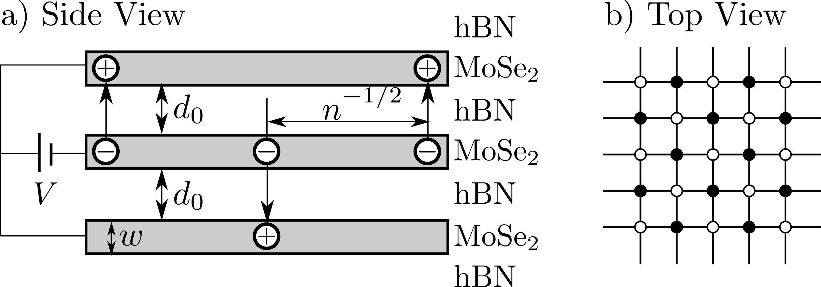 Figure 1
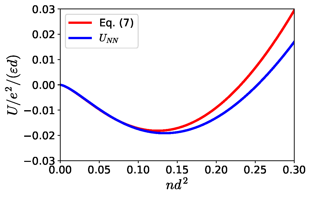 Figure 2
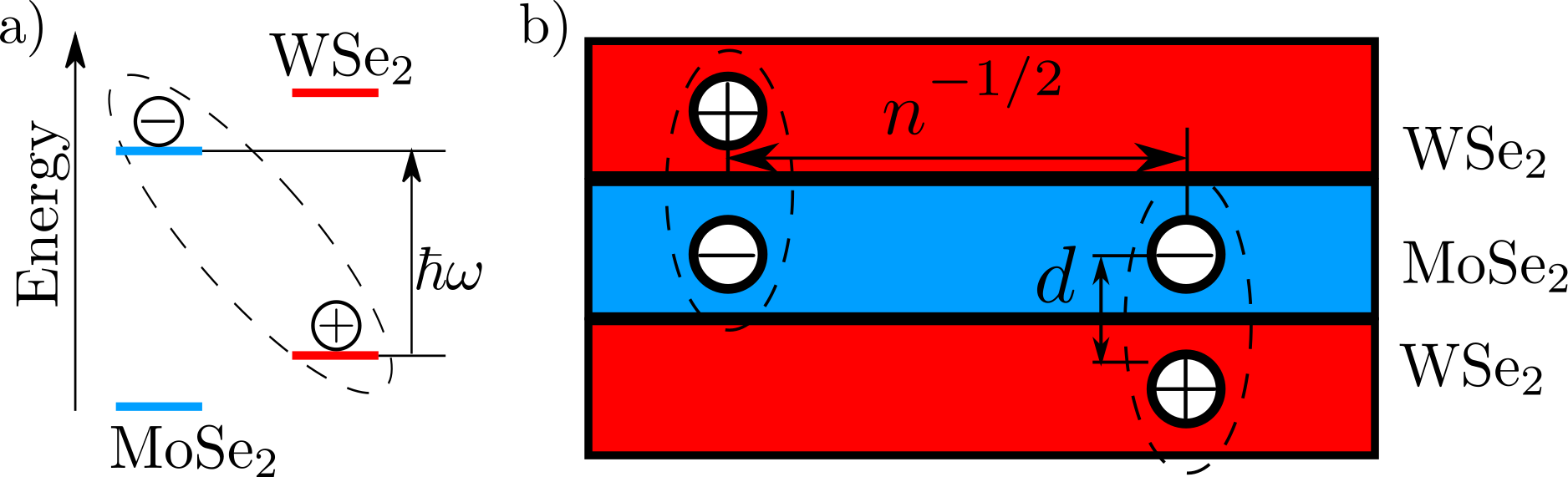 Figure 3
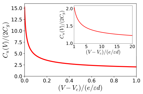 Figure 4
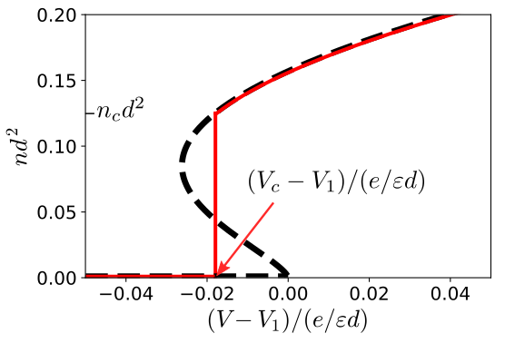 Figure 5
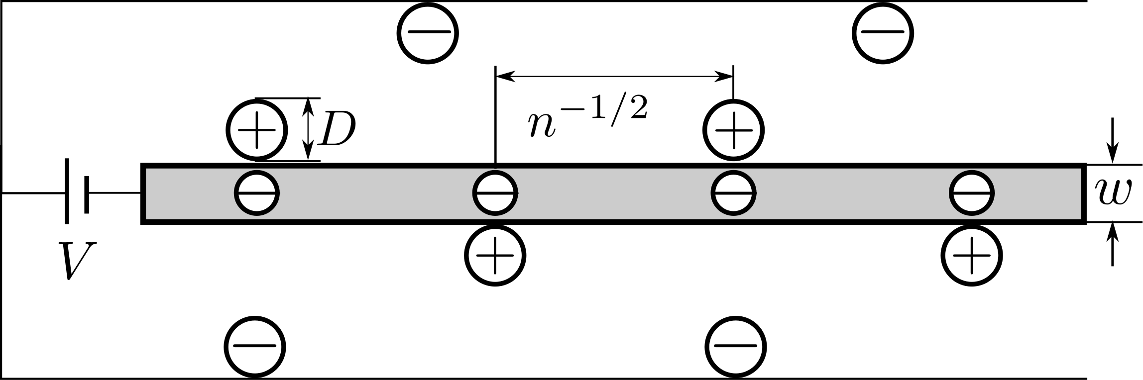 Figure 6
Peer Reviews
No public reviews on file for this paper yet. If you reviewed it on a platform where reviews are public (OpenReview, ICLR, NeurIPS, ICML), you can paste yours below so the community can read it here.
Videos
No videos yet. Explain this paper in a talk, walkthrough, or lecture? Add one.
Attraction of indirect excitons in van der Waals heterostructures with three semiconducting layers
M. Sammon
School of Physics and Astronomy, University of Minnesota, Minneapolis, MN 55455, USA
B. I. Shklovskii
School of Physics and Astronomy, University of Minnesota, Minneapolis, MN 55455, USA
Abstract
We study a capacitor made of three monolayers of transition metal dichalcogenide (TMD) separated by hexagonal Boron Nitride (hBN). We assume that the structure is symmetric with respect to the central layer plane. The symmetry includes the contacts: if the central layer is contacted by the negative electrode, both external layers are contacted by the positive one. As a result a strong enough voltage induces electron-hole dipoles (indirect excitons) pointing towards one of the external layers. Antiparallel dipoles attract each other at large distances. Thus, the dipoles alternate in the central plane forming a 2D antiferroelectric with negative binding energy per dipole. The charging of a three-layer device is a first order transition, and we show that if is the critical voltage required to create a single electron-hole pair and charge this capacitor by , the macroscopic charge ( is the device area) enters the three-layer capacitor at a smaller critical voltage . In other words, the differential capacitance is infinite at . We also show that in a contact-less three-layer device, where the chemically different central layer has lower conduction and valence bands, optical excitation creates indirect excitons which attract each other, and therefore form antiferroelectric exciton droplets. Thus, the indirect exciton luminescence is red shifted compared to a two-layer device.
In a standard parallel-plate capacitor, the capacitance is equal to the “geometric capacitance” (in Gaussian units), where is the dielectric constant of the medium separating the two plates, is the area of each plate, and is the distance between them. The expression is correct when both electrodes are made from a “perfect” metal, which by definition screens the electric field with a vanishing screening radius. This condition fails if both sides of the capacitor are made of a layer of an intrinsic semiconductor and the applied voltage generates in them an equal small density of a two-dimensional electron (2DEG) and hole (2DHG) gas. For example, one can think about two separately contacted monolayers of intrinsic MoSe2 separated by a few hexagonal boron nitride (hBN) layers with total width . If in both the 2DEG and the 2DHG , where is the carrier Bohr radius and is its effective mass, electrons and holes created in opposite MoSe2 layers can be treated as classical point like particles. It was shown Skinner and Shklovskii (2010) that if in addition , the capacitor charge grows with as , where
[TABLE]
is the critical voltage required to create a single isolated electron-hole pair in an intrinsic semiconductor, is the bandgap of the semiconductor, and is the binding energy of the electron-hole pair. The differential capacitance becomes much larger than and grows as with decreasing . As a function of the capacitance .
This anomalous capacitance growth near is due to the fact that each electron in the 2DEG is bound to a hole in the 2DHG of the other layer, forming an indirect exciton with a dipole moment . At , parallel dipoles are separated from each other by a large distance. Therefore, their repulsion is weak and provides a weak resistance to further capacitor charging leading to a diverging capacitance as from above. A similar anomalously large capacitance was predicted when one layer is replaced by a metallic plane. Skinner and Shklovskii (2010) A capacitance 40% larger than the geometrical value, which may be a result of this phenomena, was reported in YBCO/LAO/STO nanostructures. Li et al. (2011) A similar effect was predicted in graphene-metal capacitors placed in a strong perpendicular magnetic field which localizes carriers. Skinner and Shklovskii (2013) A capacitance that is larger than the geometrical one was observed in this case. Skinner et al. (2013)
The strong capacitance anomaly in the two-layer device is due to the discreteness of charge and their strong correlations at small densities . In this paper we explore similar correlation physics in three-layer devices with a symmetry plane. For example, we may think about three monolayers of intrinsic MoSe2 each of width , separated by the same number of hBN layers of total width on each side, so that the structure is symmetric with respect to the central layer midplane. The symmetry is not only geometrical, but also includes the voltage contacts: if the central layer is contacted by the negative electrode, both external layers are contacted by the positive electrode. Correspondingly, an equal number of voltage induced indirect excitons, each with a dipole moment , are directed from the central plane to the top and to the bottom (see Fig. 1a). At large distances along the plane, two antiparallel dipoles attract each other, while at distances smaller than they repel each other. It is natural to assume that as a result the dipoles form a two-dimensional antiferroelectric square lattice. This lattice is similar to NaCl, where Na-like and Cl-like sites are occupied by up and down pointing dipoles, i.e. all nearest neighbor dipoles are antiparallel (see Fig. 1b) . Electrons of the central plane form a square lattice with the lattice constant .
We show below that at low temperatures when the applied voltage grows, the attraction between indirect excitons in the three-layer device causes a first order phase transition (see Fig. 2). While at small there are no dipoles and the capacitor remains uncharged, at some critical value the whole lattice of alternating dipoles emerges. This means that a macroscopic charge , where and is the device area, enters this capacitor. Thus, the differential capacitance has a -peak at . At , as continues to grow the capacitance slowly approaches its normal geometric value . The giant -peak of the capacitance at can be thought of as an enhanced version of the anomaly near predicted for a two-layer capacitor.Skinner and Shklovskii (2010) A similar -peak capacitance was predicted in a 3D nanocrystal film gated by an ionic liquid in which the ions penetrate between nanocrystals. Chen et al. (2011)
For a quantitative description of the three-layer capacitor we assume the density is such that so that we may treat all charges classically. The differential capacitance of such a device can be determined from the total electrostatic energy of the system as
[TABLE]
The energy of this system of classical charges can be written as
[TABLE]
where is the voltage necessary to create a single isolated electron-hole pair and is given by Eq. (1), while is the interaction energy per electron-hole pair in the system. We can further separate the interaction energy as , where is the contribution to from the electrons interacting with all other charges, while is the contribution to from the holes interacting with all other charges. It should be clarified that in and we neglect the interaction between electrons and holes of the same pair. Assuming the electrons and holes can be treated classically, the binding energy in Eq. (1) is given by . Here and below we use the Coulomb potential with an effective dielectric constant which is close to the dielectric constant of hBN. This effective medium potential was used in previous studies of electron-hole interactions in bilayer TMD heterostructures separated by several layers of hBN,Fogler et al. (2014) and is in contrast with the Rytova-Keldysh potential used for a single TMD layer in air. Its use for our system can be justified because the distance between neighboring dipoles is much larger than the distance at which the electric field lines spread over the entire structure. Here the factor 2 comes from the ratio of the dielectric constant of MoSe2 and hBN, and is the thickness of a monolayer of MoSe2.
Each hole in an external plane pairs with an electron in the central plane in such a way that the orientation of the dipoles alternates between nearest neighbor sites of the electrons in the central plane square lattice, as shown in Fig. 1(b). Let us consider the electron-hole pair located at the central white site in Fig. 1(b). For the electron at the origin, we can write
[TABLE]
where is an index labeling the electron lattice sites, is defined as the origin, and is the distance between site and the origin. The factor accounts for the double counting when computing the interaction energy . For the hole that is also located at the origin, we can use the fact that the electron and hole form a dipole with a particular orientation (in this case upwards) to separate as . Here
[TABLE]
is the contribution from the interaction of the hole with dipoles with the same orientation as the origin dipole (white sites), while
[TABLE]
is the contribution from the interaction of the hole with dipoles of the opposite orientation(black sites). The symbols next to the summation indicate that the sums are restricted to the corresponding sublattice shown in Fig. 1(b). Upon inspection, it is clear that Eqs. (4) and (5) are similar so that we can write as
[TABLE]
where
[TABLE]
and
[TABLE]
and we have rewritten the site index using the integers and of the electron lattice coordinates in units of . For the summation over the black sublattice in Eq. (9), we restrict ourselves to values of and such that is odd. Both summations are convergent for any . The results of this summation are shown by the red curve in Fig. 3 as a plot of vs . We see that the interaction energy is negative for a finite range of densities due to the attraction between nearest neighbor dipoles with opposite orientation. At it reaches a minimum value of . In order to better understand this, we compare this result to the energy obtained from only the nearest neighbor sites of each sublattice, shown by the labeled curve (blue curve) in Fig. 3. We see that for small the energy is almost completely determined by these nearest neighbors, with significant deviation only appearing beyond the minimum of .
Once the energy is found, we can find the voltage as
[TABLE]
Our main result is shown in Fig. 2 as a plot of the density as a function of the voltage . The dashed curve is obtained from Eq. (10). Most noticeable is that there is a range in which there are three densities for each voltage: a lower branch along , a middle branch, and an upper branch. Within the middle branch, the capacitance defined by Eq. (2) is negative and this region is thermodynamically unstable and is inaccessible. Thus in experiment, we do not expect the density to change continuously along the dashed curve, but instead along the curve shown in red where the density jumps to a value
[TABLE]
at a critical voltage
[TABLE]
Here is determined by Maxwell area ruleLandau and Lifshitz (1980)
[TABLE]
where the integral is taken along the dashed curve in Fig. 2. At the two regions lying between the vertical red line and the dashed curve have equal area. This rule is well known for the van der Waals liquid-gas pressure-volume isotherm. 111In this analogy, plays the role of volume while the voltage plays the role of pressure. It is worth noting that obtained from Maxwell’s area rule is the same at which reaches its minimum value. As the density abruptly jumps, there is a -peak in the capacitance at . For we can write the capacitance as
[TABLE]
where the non-singular capacitance is obtained by differentiating the upper branch of the curve shown in Fig. 2 with respect to and is shown in Fig. 4. As approaches from above, grows as , and attains a very large maximum value , where is the geometrical capacitance of the capacitor formed by either the central and upper planes or the central and lower planes. At larger voltages it approaches corresponding to the geometric value of the three-layer system as shown in the inset of Fig. 4.
So far we have been dealing with very low temperatures and have ignored disorder. Temperature and disorder smear the -function as well as the low voltage peak of the non-singular large voltage tail of . When the width of the -function reaches , the two peaks in the capacitance merge to form a single peak. Because this happens at , a very large peak of the capacitance (much larger than in the case of two layers) survives in the presence of disorder or higher temperatures. It is easy to imagine that the measured capacitance peak is 5-10 times larger than the geometrical value. The reason for the early merging of the -function with the non-singular peak is that the optimal distance between electrons in the central plane is relatively large and makes both the optimal energy and the voltage scale of the dipole configuration in Fig. 2 relatively small. We can estimate the scale of temperature at which thermal fluctuations destroy the effect from the minimum in the interaction energy shown in Fig. 3. For and nm for a three layer thick hBN spacer, we find at K thermal fluctuations begin to dominate.
We have also ignored quantum effects. Typically the localization length of electrons in the central plane can be comparable with , so that quantum effects may modify the energy of the three-layer system at large enough even at zero temperature and disorder. Fogler et al. (2014) However, even in such a case, at small the energy of the electron-hole dipoles (excitons) is dominated by their dipole-dipole attraction and charging occurs by the first order transition. Quantum mechanics can still somewhat reduce and . Quantum Monte-Carlo simulations similar to those in Refs. [De Palo et al., 2002; Schleede et al., 2012; Maezono et al., 2013] are necessary to address these changes quantitatively.
Devices similar to those shown in Figs. 1 and 5 can be also made from graphene monolayers, however in this case the classical model leading to attraction between indirect excitons becomes useful only in strong magnetic fields such that , where is the magnetic length. In devices with this condition may substantially reduce .
Three-layer devices made of MoSe2 can face difficulties in making separate contacts to all three layers. Therefore, a similar device made of a single MoSe2 monolayer gated from both sides by an ionic liquid can be more attractive. In this case the dipoles are formed by electrons of the MoSe2 monolayer bound to excessive positive ions, which stick to the monolayer in alternating positions above and below it (see Fig. 5). At small electron densities such a device is quantitatively similar to the three layer device described with a dipole moment , where is the ionic diameter.
Above we talked about the capacitance of three-layer devices. Three-layer devices can be also used for optical studies of spatially indirect interacting excitons. It has been shownRivera et al. (2015); Calman et al. (2019) that in bilayer MoSe2/WSe2 structures, the type II band alignment of the MoSe2 and WSe2 monolayers allows the formation of indirect excitons, in which an electron in MoSe2 binds to a hole in WSe2 (see Fig.6a). Because of the weak overlap of the electron and hole wavefunctions, these excitons decay slowly enough to form the ground state which minimizes their repulsion. In the photoluminescence experiments on the MoSe2/WSe2 device of Ref. [Rivera et al., 2015], it was observed that the indirect exciton luminescence line blueshifts as the intensity of the laser increases due to the dipole-dipole repulsion of the indirect excitons. In a trilayer device,Baranowski et al. (2017); Choi et al. (2018) such as WSe2/MoSe2/WSe2 (and similar devices with symmetric hBN spacers), we instead predict an attractive interaction between indirect excitons formed from opposite WSe2 layers (see Fig. 6b). At low illumination intensities these excitons condense into droplets of density which do not interact with each other. These droplets are different from the exciton droplets in 3D semiconductors proposed by Keldysh and Kozlov.Keldysh and Kozlov (1968) Those droplets are formed by the van der Waals attraction between excitons and occurs when the excitons are at distances of order . Our droplets are the result of the electrostatic dipole-dipole interaction and the excitons are separated by the larger than distance set by our classical theory. In such a device, the luminescence peak should be redshifted. 222We can extrapolate the classical energy of a crystal of alternating dipoles to estimate the redshift as meV, where we have used and for monolayer TMDs.Laturia et al. (2018) The luminescence line of excitons in these droplets should not change with the laser intensity until the intensity becomes so large that the droplets fill the entire sample.
We are grateful to L. V. Butov, M. M. Fogler, Q. Shi, and B. Skinner for useful discussions. M. Sammon was supported primarily by the NSF through the University of Minnesota MRSEC under Award No. DMR-1420013.
The reference list from the paper itself. Each links out to its DOI / PubMed record.
- 1Skinner and Shklovskii (2010) B. Skinner and B. I. Shklovskii, Phys. Rev. B 82 , 155111 (2010).
- 2Li et al. (2011) L. Li, C. Richter, S. Paetel, T. Kopp, J. Mannhart, and R. C. Ashoori, Science 332 , 825 (2011).
- 3Skinner and Shklovskii (2013) B. Skinner and B. I. Shklovskii, Phys. Rev. B 87 , 035409 (2013).
- 4Skinner et al. (2013) B. Skinner, G. L. Yu, A. V. Kretinin, A. K. Geim, K. S. Novoselov, and B. I. Shklovskii, Phys. Rev. B 88 , 155417 (2013) . · doi ↗
- 5Chen et al. (2011) T. Chen, B. Skinner, and B. I. Shklovskii, Phys. Rev. B 84 , 245304 (2011) . · doi ↗
- 6Fogler et al. (2014) M. M. Fogler, L. V. Butov, and K. S. Novoselov, Nat. Comm. 5 , 4555 (2014).
- 7Landau and Lifshitz (1980) L. D. Landau and E. M. Lifshitz, “Statistical physics part 1,” (Pergamon Press Inc., 1980) Chap. 84, pp. 261–262, 3rd ed.
- 8Note (1) In this analogy, n 𝑛 n plays the role of volume while the voltage V 𝑉 V plays the role of pressure.