Electron interferometry and quantum spin Hall phase in silicene
Bart{\l}omiej Rzeszotarski, Alina Mre\'nca-Kolasi\'nska, and, Bart{\l}omiej Szafran

TL;DR
This paper explores electron interferometry in silicene to detect the quantum spin Hall phase, demonstrating how interference patterns change with topological states and external fields.
Contribution
It introduces a device concept using two-path electron interference in silicene to identify topological insulator phases through conductance features.
Findings
Quantum spin Hall phase suppresses interference due to spin current separation.
Normal transport shows Aharonov-Bohm oscillations.
Localized resonances appear in conductance during the topological phase.
Abstract
We discuss devices for detection of the topological insulator phase based on the two-path electron interference. For that purpose we consider buckled silicene for which a local energy gap can be opened by vertical electric field to close one of the paths and for which the quantum spin Hall insulator conditions are controlled by the Fermi energy. In quantum spin Hall phase the interference is absent due to the separation of the spin currents and the conductance of the devices include sharp features related to localized resonances. In the normal transport conditions the two-path interference produces a regular Aharonov-Bohm oscillations in the external magnetic field.
Click any figure to enlarge with its caption.
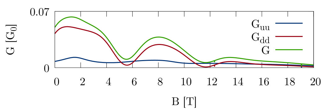 Figure 1
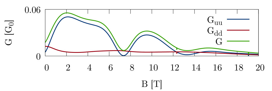 Figure 2
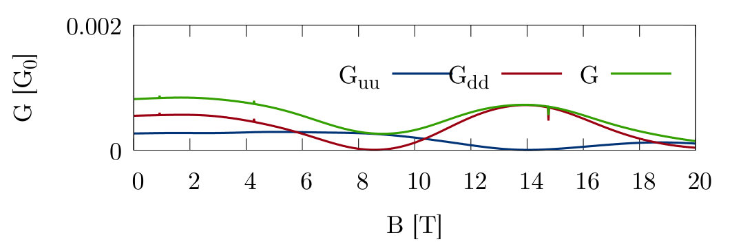 Figure 3
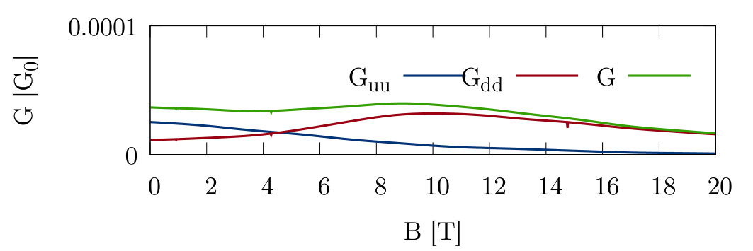 Figure 4
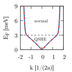 Figure 5
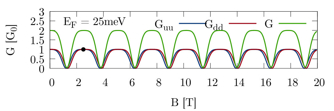 Figure 6
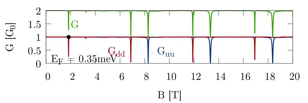 Figure 7
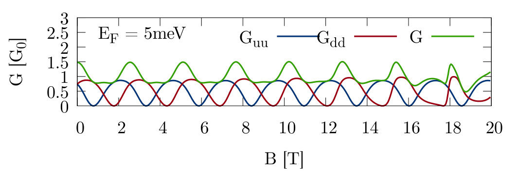 Figure 8
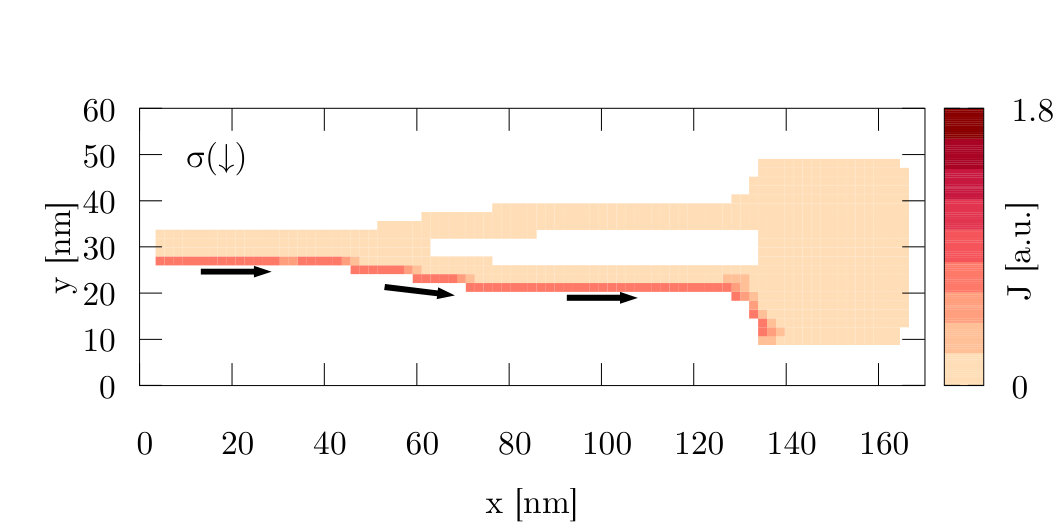 Figure 9
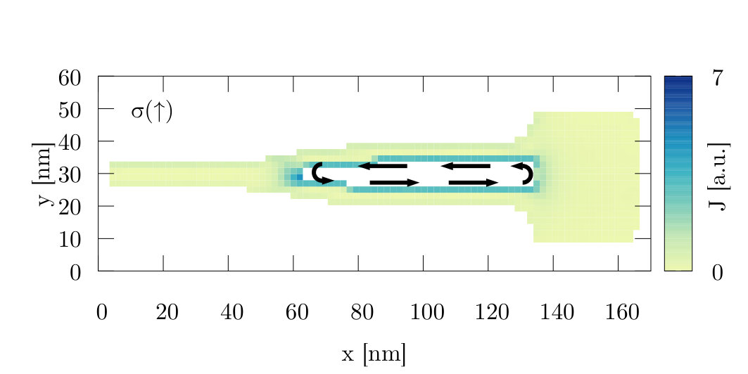 Figure 10
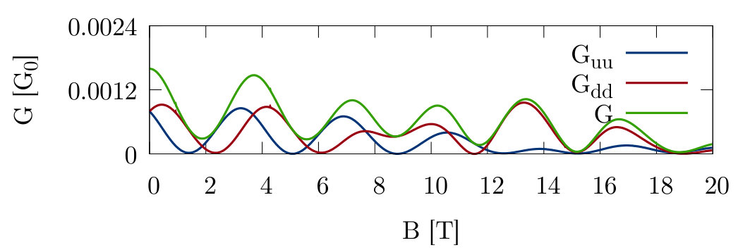 Figure 11
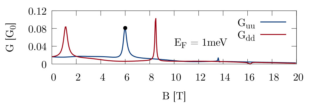 Figure 12
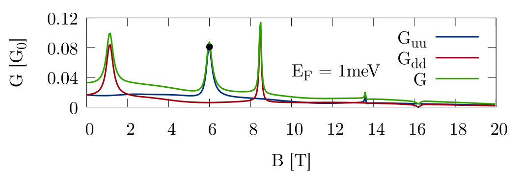 Figure 13
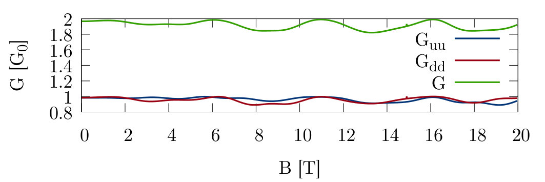 Figure 14
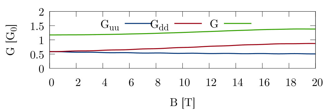 Figure 15
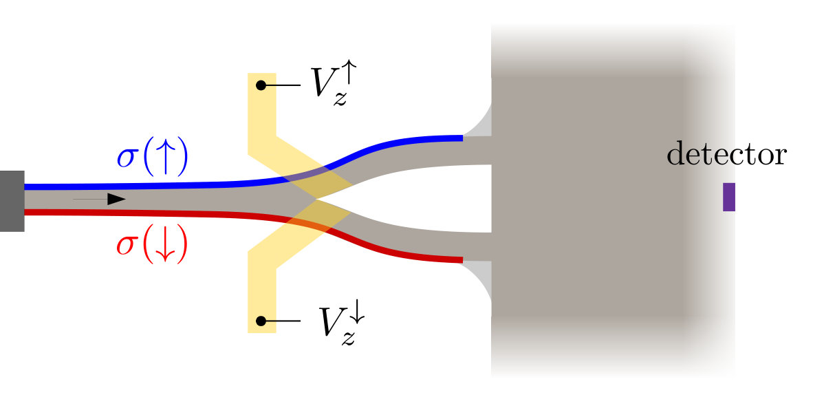 Figure 16
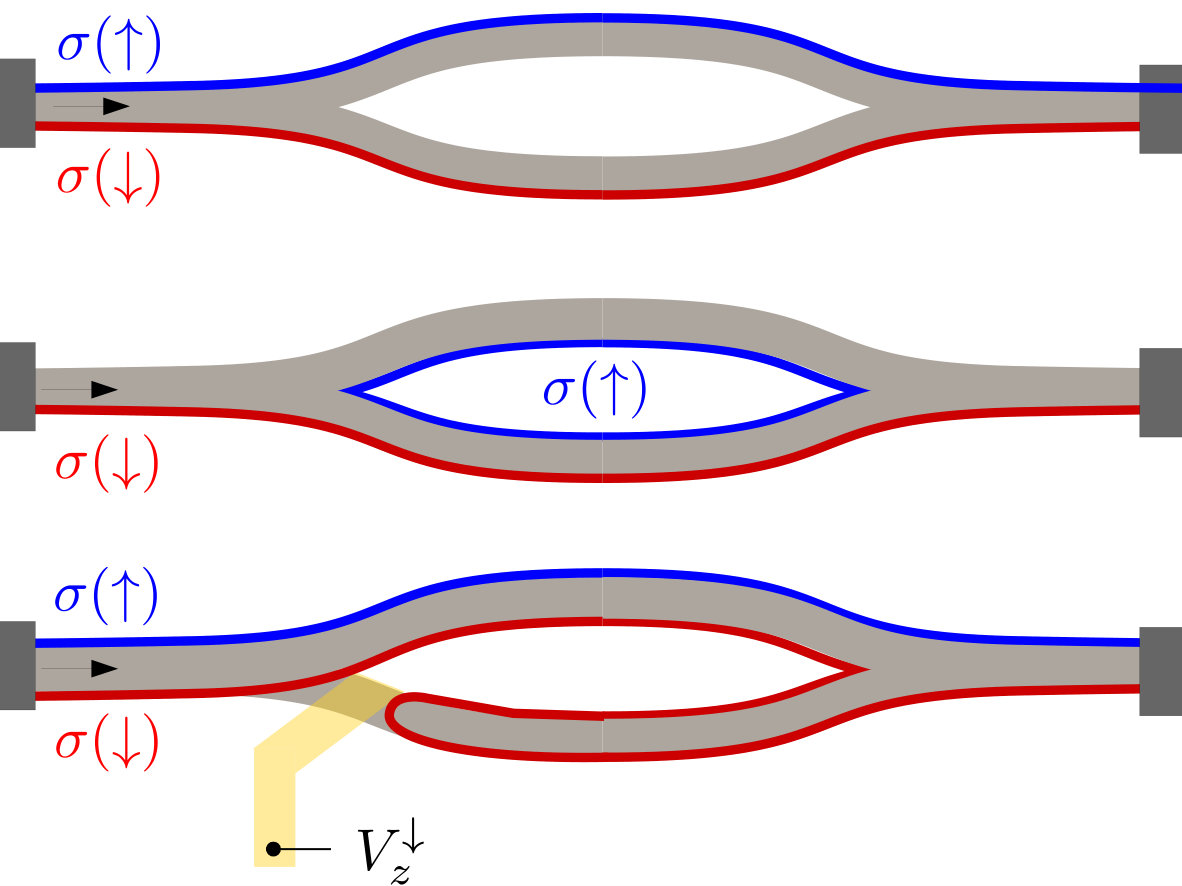 Figure 17
Peer Reviews
No public reviews on file for this paper yet. If you reviewed it on a platform where reviews are public (OpenReview, ICLR, NeurIPS, ICML), you can paste yours below so the community can read it here.
Videos
No videos yet. Explain this paper in a talk, walkthrough, or lecture? Add one.
Electron interferometry and quantum spin Hall phase in silicene
Bartłomiej Rzeszotarski
AGH University of Science and Technology, Faculty of Physics and Applied Computer Science,
al. Mickiewicza 30, 30-059 Kraków, Poland
Alina Mreńca-Kolasińska
AGH University of Science and Technology, Faculty of Physics and Applied Computer Science,
al. Mickiewicza 30, 30-059 Kraków, Poland
Bartłomiej Szafran
AGH University of Science and Technology, Faculty of Physics and Applied Computer Science,
al. Mickiewicza 30, 30-059 Kraków, Poland
Abstract
We discuss devices for detection of the topological insulator phase based on the two-path electron interference. For that purpose we consider buckled silicene for which a local energy gap can be opened by vertical electric field to close one of the paths and for which the quantum spin Hall insulator conditions are controlled by the Fermi energy. In quantum spin Hall phase the interference is absent due to the separation of the spin currents and the conductance of the devices include sharp features related to localized resonances. In the normal transport conditions the two-path interference produces a regular Aharonov-Bohm oscillations in the external magnetic field.
Quantum spin Hall (QSH) insulators r1 ; r2 ; r3 form a class of two-dimensional topological insulators with bulk energy gap and topologically protected currents of a fixed spin-orbital helicity. The QSH phase r4 is discussed for bulk nanostructures including HgTe quantum wells r6 ; r7 ; r8 ; r9 and InAs/GaSb interfaces r10 ; r11 as well as graphene-like monolayer Xenes materials r12 ; r13 , including silicene silitmdc ; chow ; Liu11 ; Liu ; Ezawa . The QSH conditions in silicene occur for the Fermi energy near the charge neutrality point silitmdc ; chow ; Liu11 ; Liu ; Ezawa . The Fermi energy in 2D monolayer materials can be controlled by external gating. In the QSH phase the spin currents are confined by opposite edges of the sample, which was used for proposals of spin sources and spin filters in silicene r28 ; r29 ; r39 ; r40 ; r42 ; r33 . In this paper we propose electron interferometer devices that can be used for detection of the QSH transport conditions. The devices are based on the idea of two-path interference and the spin separation by the split silicene ribbon r28 . We consider a double slit interference device as well as a quantum ring and find that in the normal phase one observes smooth Aharonov-Bohm conductance oscillations while in the QSH regime only sharp conductance features due to the localized resonances with circular current loops are observed. In silicene both the localized resonances and the Aharonov-Bohm oscillations can be intentionally switched off by applying a local electric field to one of the arms of the split channels, due to the buckling of the crystal lattice that translates the electric field into a local energy gap fie1 ; fie2 that stops the current flow.
The schematics of the double slit interferometer depicted in [Fig. 1(a)]. The electrons are fed from the left by the silicene ribbon of a zigzag edge of 6.5 nm width. The zigzag ribbon supports the spin-polarized edge transport at the Fermi energy meV with respect to the charge neutrality point [see the dispersion relation in Fig. 1(b)]. In the quantum spin Hall insulator phase the opposite spin currents flow at the opposite edges of the ribbon [see Fig. 1(a)]. The input lead splits into two channels of the same width. In the topological phase this spindle-shaped connection separates the opposite spin currents to the two channels [Fig. 1(a)]. The split channels are connected to semi-infinite open plane of silicene [Fig. 1(a)] with a smoothed extensions that prevent backscattering. At open halfplane the areas marked by the gray color fading to white in Fig. 1(a) we attach wide silicene ribbons that make the edges of the computational box reflectionless. For meV [Fig. 1(b)] the current flows through the bulk of channel for both spin orientations and we refer to these conditions as the normal phase. In the normal phase the current flows through both the split channel for both spin orientations. The Young interference of the waves entering the open halfplane by different slits can only occur in the normal phase. In the topological phase each of the slits feeds opposite spin. Thus, observation of the Young interference should depend on the Fermi energy. In order to monitor the interference in the model device [Fig. 1] at 32 nm to the right of the slit opening a zigzag ribbon of width 6.5 nm is connected as a detector kka . In order to gain additional control in the interference device we introduce local gates (yellow gates in Fig. 1) to switch off the currents.
We use the tight-binding Hamiltonian spanned on orbitals of Si atoms Liu
[TABLE]
where () is the creation (annihilation) operator for an electron on atom with spin . The calculation accounts for hexagonal lattice of Si atoms with constant Å and a vertical shift of 0.46 Å between the A and B sublattices. Summations over and run over nearest and next nearest neighbor ions, respectively. In Eq. (1) we use eV for the hopping energy Liu ; Ezawa , meV Liu is the intrinsic spin-orbit coupling energy r4 where () for the clockwise (counterclockwise) next-nearest neighbor hopping, meV is the intrinsic spin-orbit coupling energy Liu ; Ezawa , where the unit vector from -th to -th ion . Within sublattice A (B) we apply (). The last term in Eq. (2) introduces a local vertical electric field (yellow gates in Fig. 1) at the entrance to the slits to intentionally switch off the currents in the channels. The gates introduce vertical electric field of about 100 mV/Å that produces the potential difference meV at the A and B sublattices of the buckled silicene lattice. The field opens the local energy gap for the Fermi energy range considered here and closes the channel for the electron flow. In presence of an external perpendicular magnetic field the Peierls phase is introduced to the hopping terms.
We derive the conductance of the device by solution of the quantum scattering problem within the Landauer approach. For the latter we use the wave function matching r33 ; Kolasiński et al. (2016) method for the atomistic description of the medium. The positive (negative) values are labeled by , (,). The Rashba interaction is weak, the spins are nearly polarized in the direction and no spin flips are obtained ( and the total conductance is a sum of spin-diagonal contributions .
Figure 2(b) shows the conductance in the absence of the electric field in the gated area in the normal phase for 5 meV. The conductance for both spin orientations and the total conductance undergo periodic oscillations in the external magnetic field with a period of about 4 T, which is the Aharonov-Bohm period for the area of about 1000 nm2 enclosed between the electron paths passing through the split channels to the detector. For the upper [Fig. 2(c)] or lower [Fig. 2(a)] channel cut off by the vertical electric field, the Aharonov-Bohm conductance oscillations disappear, which is a signature of the switched off two-slit interference.
In the QSH phase [Fig. 3(b)] we do not observe the regular AB oscillations even for both channels open. The wave function for each spin passes through a single slit to the halfplane, so no Young interference can occur. Instead, in Fig. 3(b) we find sharp peaks of conductance which correspond to localized resonances with the current circulation around the etched area [see Fig. 4(b) for the point marked by the dot in Fig. 3(b)]. The local electric field which cuts off the upper or lower channels excludes the current circulation, and the rapid features of the conductance dependence on the external field disappear [Fig. 3(a,c)]. For one of the channels closed [Fig. 3(a,c)] the dominant spin in the detector is somewhat counterintuitive: when the lower channel – preferred by the spin-down currents – is closed the calculated is much larger than [Fig. 3(a)] for a general . The reason for this is that for the spin-down current is directed to the upper channel, where it flows near its lower edge, thus closer to the detector.
Similar control of the two-path interference effects can be obtained in a quantum ring [Fig. 5] formed by reflection of the split channel of Fig. 1(a). The calculated conductance in the QSH regime is given in Fig. 6(a) for meV. For a general magnetic field the system is transparent for the electron flow [Fig. 5(a)]. Sharp dips of conductance appear [Fig. 6(a)] by interference with the localized loops of current stabilized near the inner edge of the ring [Fig. 5(b)]. Note that in the open system conductance peaked by interference with localized states, because signal received by detector came from leakage [Fig. 3(b)] of the resonant current loop. The localized resonances are only weakly coupled to the leads hence their long lifetime that is translated to narrow width of the resonances. In the normal transport conditions [Fig. 6(b,c)] no sharp resonances appear and smooth AB oscillations appear with the period independent of the energy. For higher energy [Fig. 6(c)] the contribution to conductance of opposite spins become equal.
For the gate that cuts off the current flow across the lower channel [Fig. 5(c)] the dips due to the localized states disappear in the QSH regime [Fig. 7(a)] and the AB oscillations are removed in the normal conditions [Fig. 7(b)]. For the normal conditions at the closed lower channel reduces the conductance significantly. In the QSH conditions both spin currents find their way to the exit of the ring, although the path for the spin down current becomes quite complex [Fig. 5(c)].
In summary, we have demonstrated that gated interference devices can be defined in silicene to allow for detection of the quantum spin Hall transport conditions by reaction of the conductance to the local electric fields closing one of the paths for the electron flow.
Acknowledgments
B.R. and A.M-K. are supported by Polish government budget for science in 2017-2021 within project "Diamentowy Grant" (Grant No. 0045/DIA/2017/46). B.R. acknowledges the support of EU Project POWER.03.02.00-00-I004/16. B.S. acknowledges the support of NCN grant DEC-2016/23/B/ST3/00821. The calculations were performed on PL-Grid Infrastructure at ACK Cyfronet AGH.
The reference list from the paper itself. Each links out to its DOI / PubMed record.
- 1(1) M.Z. Hasan and C.L. Kane, Rev. Mod. Phys. 82 , 3045 (2010).
- 2(2) Jens H Bardarson and Joel E Moore, Rep. Prog. Phys. 76 056501 (2013).
- 3(3) Xiao-Liang Qi and Shou-Cheng Zhang, Rev. Mod. Phys. 83 , 1057 (2011).
- 4(4) C.L. Kane and E.J. Mele, Phys. Rev. Lett. 95 , 226801 (2005); 95 , 146802 (2005).
- 5(5) B.A. Bernevig T.L. Hughes, S.-C. Zhang, Science 314 , 1757 (2006).
- 6(6) M. König, S. Wiedemann, C. Brüne, A. Roth, H. Buhmann, L.W. Molenkamp, X.-L. Qi, and S.-C. Zhang, Science 318 , 766 (2007)
- 7(7) A. Roth, C.Brüne, H. Buhmann, L.W. Molenkamp, J. Maciejko, X.-L. Qi, S.C. Zhang, Science 32 5, 294 (2009).
- 8(8) C. Brüne, A. Roth, H. Buhmann, E. M. Hankiewicz, L.W. Molenkamp, J. Maciejko,X.L. Qi, S.C. Zhang, Nature Physics 8 , 486 (2012).