Dielectric Resonator Method For Determining Gap Symmetry Of Superconductors Through Anisotropic Nonlinear Meissner Effect
Seokjin Bae, Yuewen Tan, Alexander P Zhuravel, Lingchao Zhang,, Shengwei Zeng, Yong Liu, Thomas A. Lograsso, Ariando T. Venkatesan, Steven M., Anlage

TL;DR
This paper introduces a non-invasive microwave resonance technique using laser scanning to image the gap nodal structure of superconductors, successfully identifying isotropic and anisotropic gap symmetries.
Contribution
The method allows imaging of superconducting gap anisotropy in unpatterned samples without complex lithography, enabling broader application to unconventional superconductors.
Findings
Detected nearly isotropic gap in Nb film with <8% anisotropy.
Identified 4-fold symmetric gap structure in YBa2Cu3O7−δ with ~12.5% anisotropy.
Validated the method's effectiveness through simulation and experimental results.
Abstract
We present a new measurement method which can be used to image gap nodal structure of superconductors whose pairing symmetry is under debate. This technique utilizes a high quality factor microwave resonance involving the sample of interest. While supporting a circularly symmetric standing wave current pattern, the sample is perturbed by a scanned laser beam, creating a photoresponse that was previously shown to reveal the superconducting gap anisotropy. Simulation and the measurement of the photoresponse of an unpatterned Nb film show less than 8\% anisotropy, as expected for a superconductor with nearly isotropic energy gap along with expected systematic uncertainty. On the other hand, measurement of a YBaCuO thin film shows a clear 4-fold symmetric image with \% anisotropy, indicating the well-known 4-fold symmetric gap nodal…
Click any figure to enlarge with its caption.
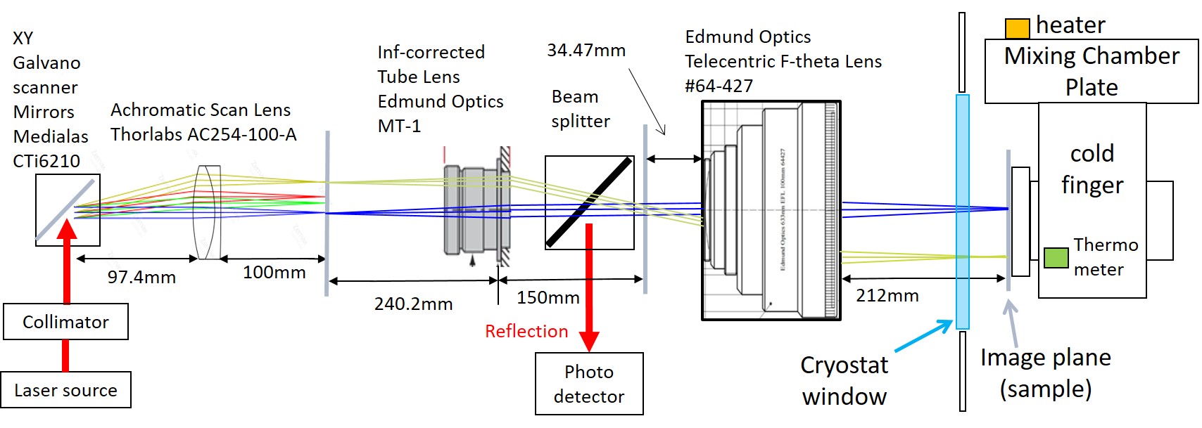 Figure 1
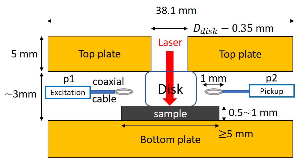 Figure 2
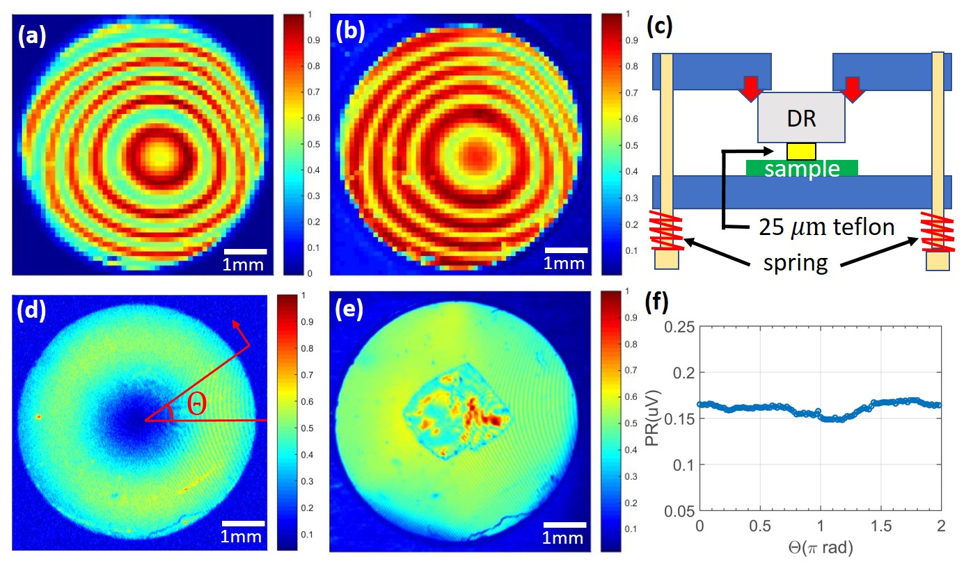 Figure 3
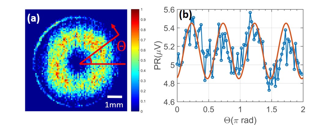 Figure 4
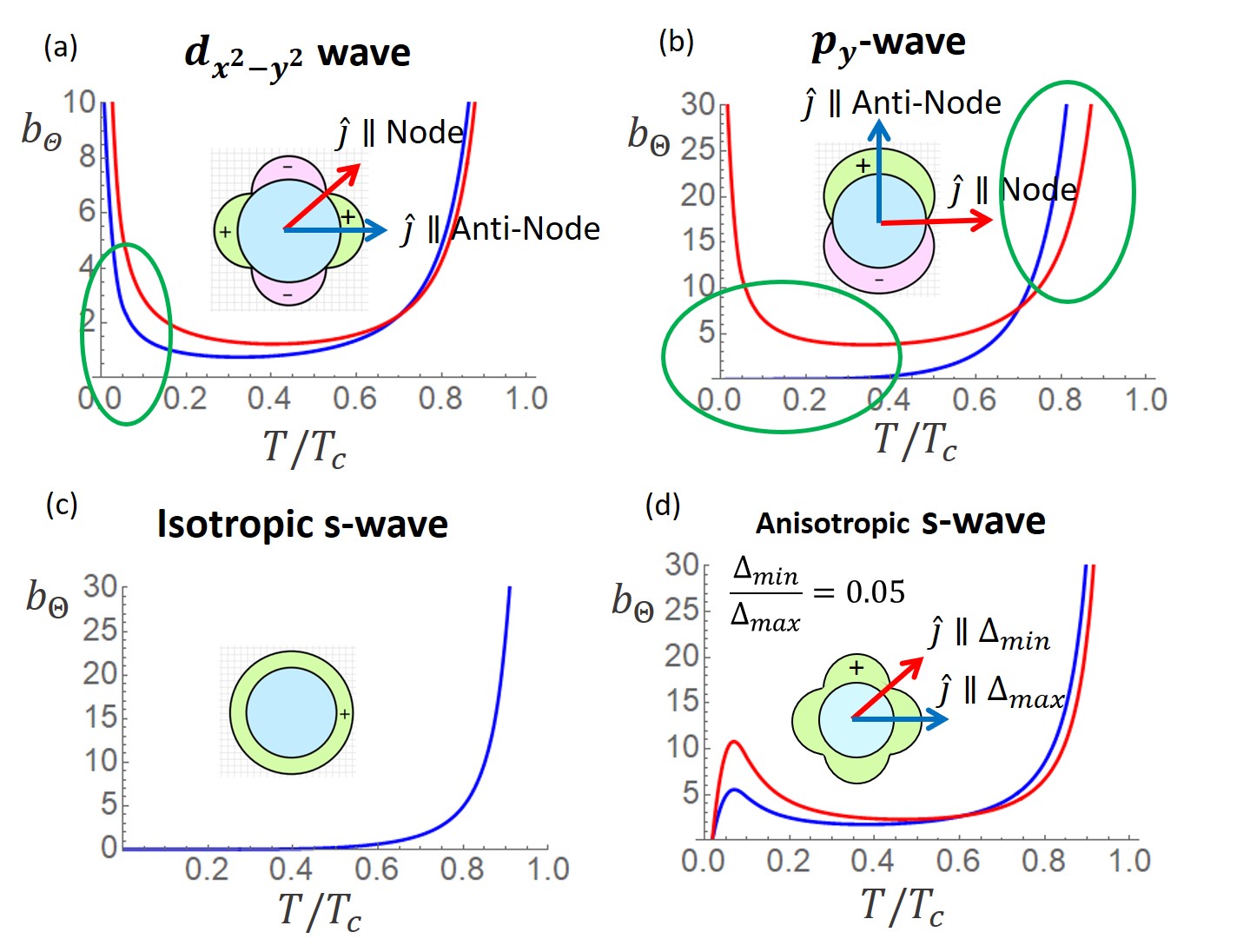 Figure 5
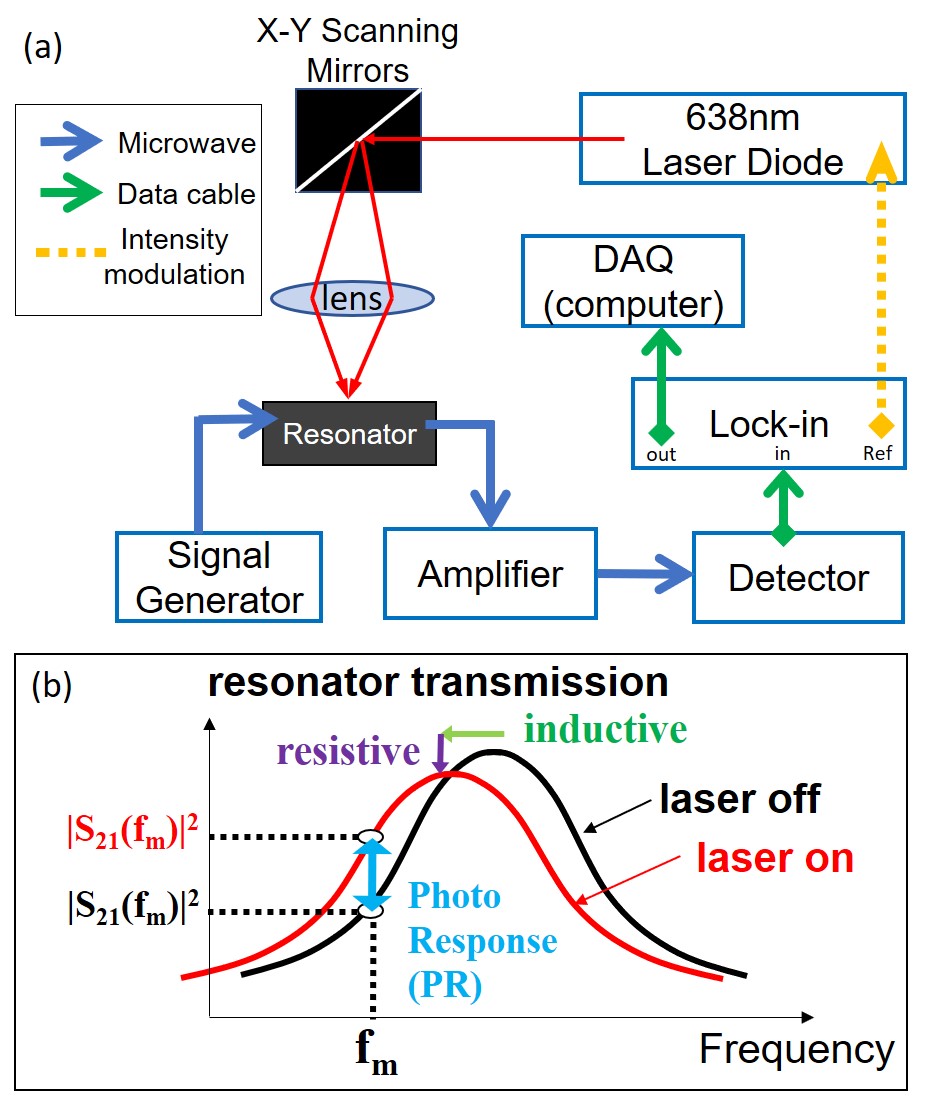 Figure 6
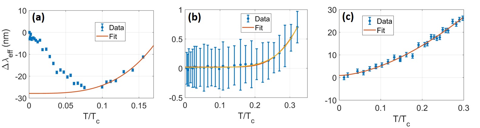 Figure 7
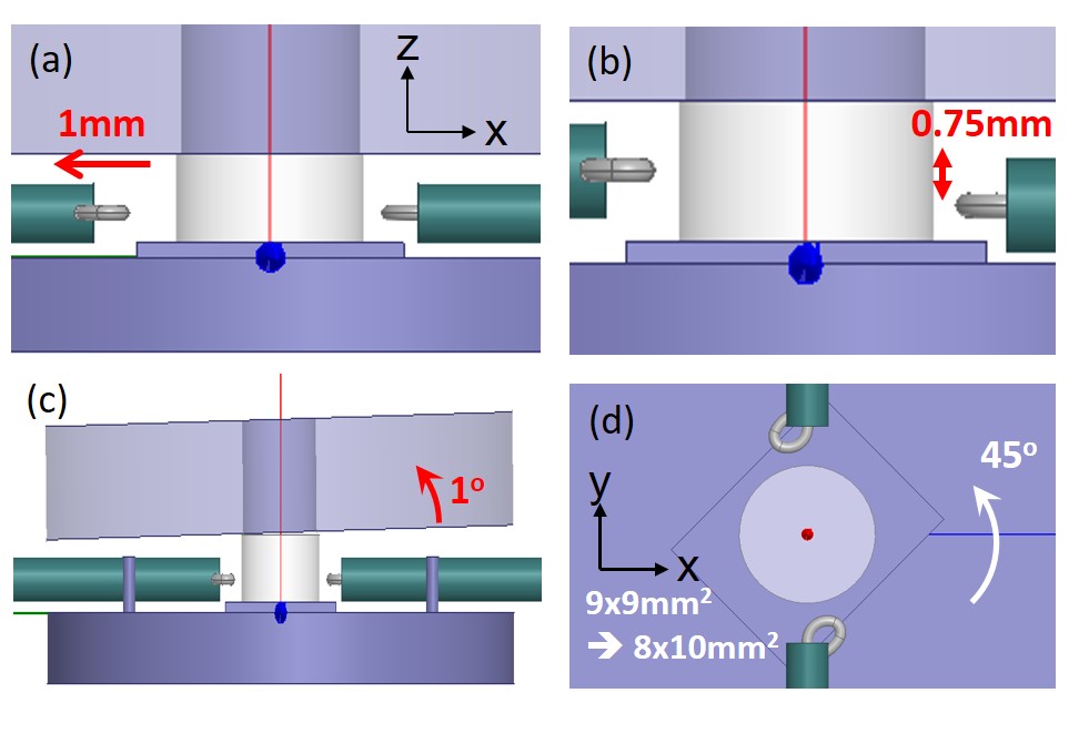 Figure 8
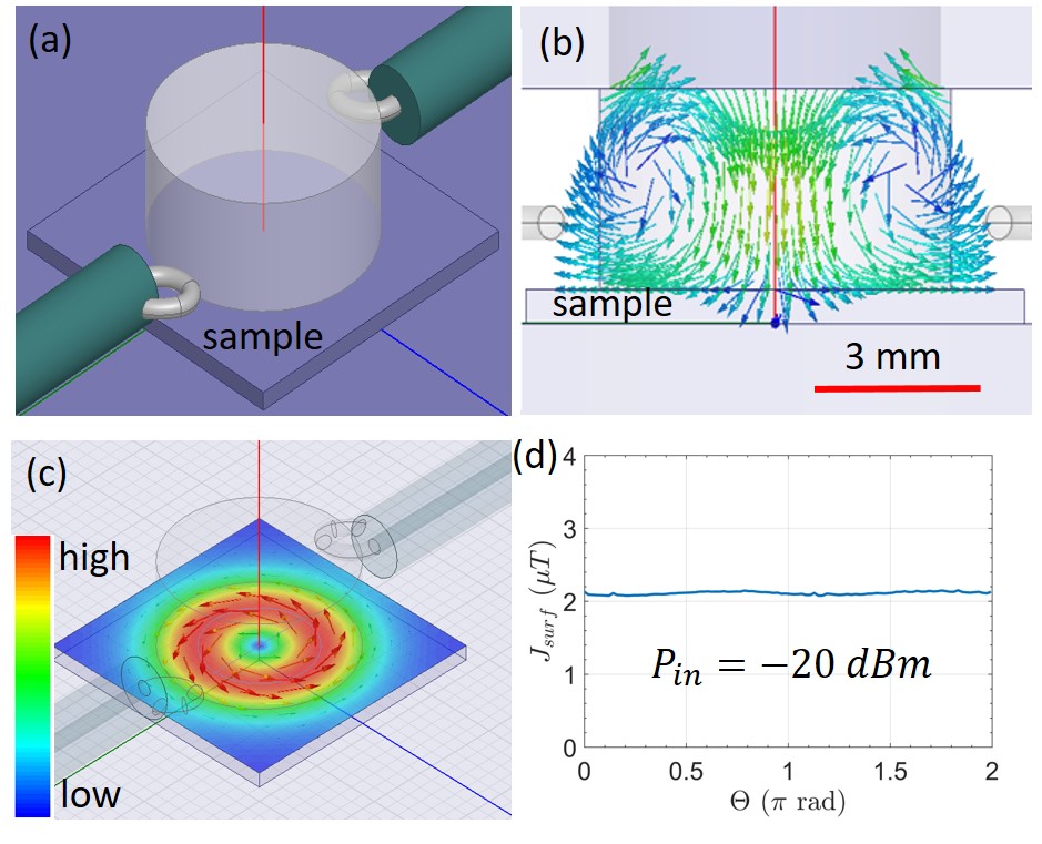 Figure 9
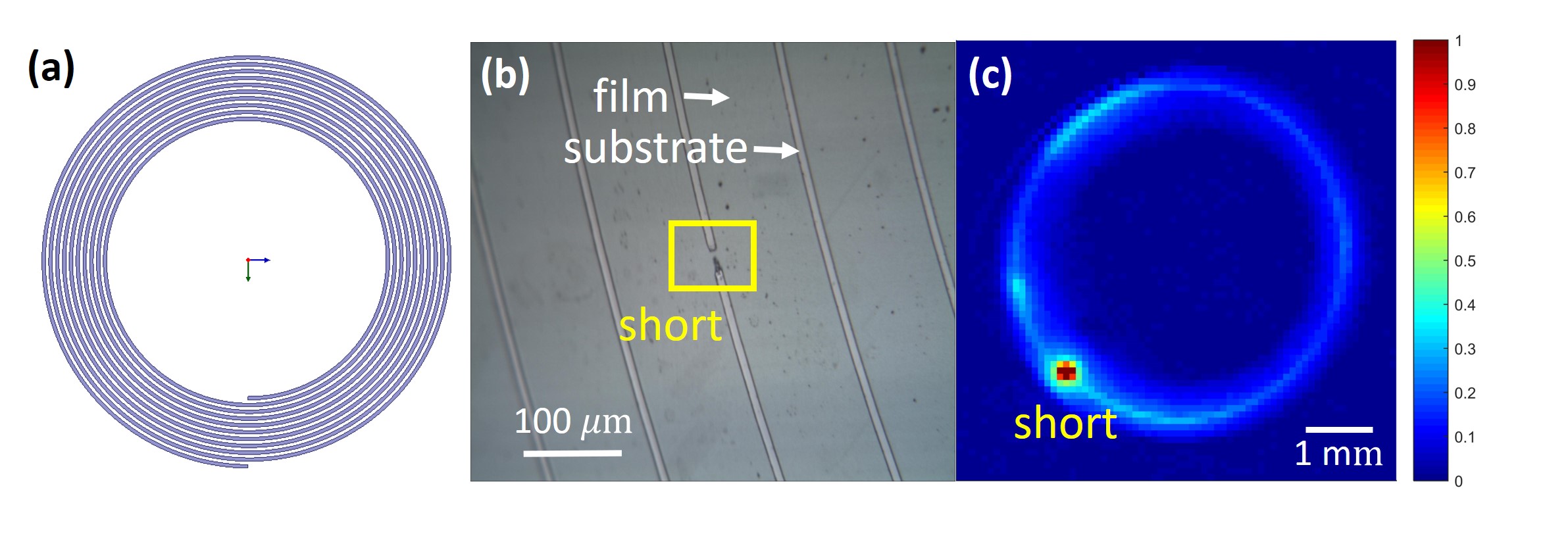 Figure 10
| Technique | Advantages | Disadvantages |
| ARPESShen et al. (1993) | Directly image band structure and gap | Requires very pristine surfaces, finite energy resolution |
| SQUIDVan Harlingen (1995) | Sensitive to the sign change of the gap | Requires high-quality tunnel junctions |
| ARSHRevaz et al. (1998) | Relatively simple thermodynamic measurement | Depends on the presence of magnetic vortices |
| Interpretation is dependent on knowledge of Fermi surface details | ||
| RamanDevereaux et al. (1994) | Able to choose specific symmetries under test by choosing polarization orientations | Requires detailed theoretical calculations of response functions for each polarization orientation to interpret data |
| aNLMEBenz et al. (2001); Oates, Park, and Koren (2004); Zhuravel et al. (2013, 2018) | Directly image gap nodal structure in real-space, not sensitive to near-surface quality | Requires high-Q resonance with circulating currents over a single-domain sample. |
Peer Reviews
No public reviews on file for this paper yet. If you reviewed it on a platform where reviews are public (OpenReview, ICLR, NeurIPS, ICML), you can paste yours below so the community can read it here.
Videos
No videos yet. Explain this paper in a talk, walkthrough, or lecture? Add one.
††thanks: Author to whom correspondence should be: [email protected]
Dielectric Resonator Method For Determining Gap Symmetry Of Superconductors Through Anisotropic Nonlinear Meissner Effect
Seokjin Bae
Center for Nanophysics and Advanced Materials, Department of Physics, University of Maryland, College Park, MD, 20742-4111, USA
Yuewen Tan
Center for Nanophysics and Advanced Materials, Department of Physics, University of Maryland, College Park, MD, 20742-4111, USA
Alexander P. Zhuravel
B. Verkin Institute for Low Temperature Physics and Engineering, National Academy of Sciences of Ukraine, UA-61103 Kharkov, Ukraine
Lingchao Zhang
Department of Physics, National University of Singapore 117551, Singapore
NUSNNI-Nanocore, National University of Singapore 117411, Singapore
Shengwei Zeng
Department of Physics, National University of Singapore 117551, Singapore
NUSNNI-Nanocore, National University of Singapore 117411, Singapore
Yong Liu
Ames Laboratory, Ames, IA 50011, USA
Thomas A. Lograsso
Ames Laboratory, Ames, IA 50011, USA
Ariando
Department of Physics, National University of Singapore 117551, Singapore
NUSNNI-Nanocore, National University of Singapore 117411, Singapore
T. Venkatesan
Department of Physics, National University of Singapore 117551, Singapore
NUSNNI-Nanocore, National University of Singapore 117411, Singapore
Steven M. Anlage
Center for Nanophysics and Advanced Materials, Department of Physics, University of Maryland, College Park, MD, 20742-4111, USA
Abstract
We present a new measurement method which can be used to image gap nodal structure of superconductors whose pairing symmetry is under debate. This technique utilizes a high quality factor microwave resonance involving the sample of interest. While supporting a circularly symmetric standing wave current pattern, the sample is perturbed by a scanned laser beam, creating a photoresponse that was previously shown to reveal the superconducting gap anisotropy. Simulation and the measurement of the photoresponse of an unpatterned Nb film show less than 8% anisotropy, as expected for a superconductor with nearly isotropic energy gap along with expected systematic uncertainty. On the other hand, measurement of a YBa2Cu3O7-δ thin film shows a clear 4-fold symmetric image with % anisotropy, indicating the well-known 4-fold symmetric gap nodal structure in the -plane. The deduced gap nodal structure can be further cross-checked by low temperature surface impedance data, which is simultaneously measured. The important advantage of the presented method over the previous spiral resonator method is that it does not require a complicated lithographic patterning process which limits one from testing various kinds of materials due to photoresponse arising from patterning defects. This advantage of the presented technique, and the ability to measure unpatterned samples such as planar thin films and single crystals, enables one to survey the pairing symmetry of a wide variety of unconventional superconductors.
pacs:
I Introduction
Among the several quantities that characterize superconductors, the superconducting gap function in momentum space is one of the most important parameters which governs the phenomenon. The symmetry of this gap function is directly related to the symmetry of the wavefunction of the superconducting electron pairs.Sigrist and Ueda (1991) Many unconventional superconductors have nodes in their superconducting gap function which are robust and arise from the symmetry of the pairing wavefunction. Thus, determining this gap nodal structure can give a significant clue about the pairing mechanism for the material.
Because of this importance, there have been numerous measurement methods developed to map out the gap structure on the Fermi surface.Tsuei and Kirtley (2000) For example, Raman scattering,Devereaux et al. (1994) angle-resolved photoemission spectroscopy (ARPES),Shen et al. (1993) angle-resolved specific heat measurement (ARSH),Aubin et al. (1997); Revaz et al. (1998); Matsuda, Izawa, and Vekhter (2006) and superconducting quantum interference device (SQUID) interferometryVan Harlingen (1995) are commonly used. However, each method has advantages and disadvantages (see Table 1) and it is best to use multiple methods to develop a consistent and complete picture of gap symmetry. ARPES and SQUID interferometry are sensitive to near-surface properties so they require very clean surfaces or high-quality tunnel barriers. Many materials present surfaces that are not characteristic of the bulk, or do not make high quality tunnel junctions, and this drawback limits them to study a relatively small number of materials. Meanwhile, ARSH and to some extent Raman scattering measure bulk response so they are free from the near-surface sensitive issue. However, they investigate quasiparticle response whose anisotropy is generally weaker than that of the superfluid response. In addition, ARSH depends on the presence of magnetic vortices. Also, to interpret the data from these methods, detailed information about the Fermi surface is required. To augment and partially overcome the limitations of these techniques, a new gap nodal spectroscopy method using the anisotropic nonlinear Meissner effect (aNLME) was proposed theoretically by Yip, Sauls, and XuYip and Sauls (1992); Xu, Yip, and Sauls (1995), Dahm and ScalapinoDahm and Scalapino (1996, 1997), and manifested in the experiment of Zhuravel et al.Benz et al. (2001); Oates, Park, and Koren (2004); Zhuravel et al. (2013, 2018) This new gap nodal spectroscopy using the aNLME gives an image of the gap nodal structure from both the bulk superfluid response and the surface Andreev bound state response, for appropriate surfaces.Zhuravel et al. (2013, 2018)
The principle of how the NLME brings out the gap nodal structure is as follows. When external magnetic field is applied to a superconductor, it generates a supercurrent to expel the fields, a hallmark of superconductivity known as the Meissner effect. The kinetic energy invested in this screening current diminishes the difference in free energy between the superconducting and normal states. In terms of Ginzburg-Landau theory, this results in a decrease in the superconducting order parameter, accompanied by a decrease in the superfluid density . As a result, the magnetic penetration depth increases correspondingly. This nonlinear effect can be parametrized in terms of the current density . In the regime where the screening current density is small compared to the zero temperature critical current density (), the nonlinearity can be expressed as followsDahm and Scalapino (1996)
[TABLE]
where is the nonlinear Meissner coefficient, represents the direction of the superfluid velocity relative to a reference direction of the gap in k-space, and is the vector current density. Note that the anisotropy of in k-space is directly determined by the nodal structure of the gap function .Dahm and Scalapino (1996, 1997) For example, if the gap function has four nodes and anti-nodes, which is the case of a -wave superconductor, is also 4-fold symmetric.Dahm and Scalapino (1996) Vice versa, if one can image the anisotropy of the in k-space, one can deduce the gap nodal structure.
II Principle of the experiment
Experimentally, to image the anisotropy in the , a thermal perturbation method is used. For the case of gap nodal superconductors such as the - or -wave cases, shows a large anisotropic temperature dependence at low temperature between situations when the direction of the current is parallel to the gap nodal and anti-nodal direction (Fig.1(a),(b)). On the other hand, for the case of an -wave or slightly anisotropic -wave superconductor, the temperature dependence of is isotropic and weak for (Fig.1(c)). However, a strongly anisotropic -wave superconductor will reveal anisotropic at low temperature (Fig.1(d)). Under a local thermal perturbation which modulates the temperature at a point on the sample, the temperature derivative of governs the sample nonlinear response. As a result of heating, the modulation in the local superfluid density inherits the anisotropy in ,Dahm and Scalapino (1997); Zhuravel et al. (2013) hence creating anisotropy in the electromagnetic response of the superconductor.
The anisotropy of the electromagnetic response can be investigated by a laser scanning microscope (LSM). As seen from Fig.2(a), a microwave signal is injected into a resonator containing a superconducting sample. Below and for specific resonant modes, a steady state circulating microwave current is induced on the surface of the sample (discussed in detail in Sec.III.1). Then, a focused scanning laser beam illuminates a small part of the sample and the laser intensity is modulated periodically in time. The illumination induces a local temperature modulation that is periodic in time. Since the local superfluid density depends on the local temperature, the temperature change brings about a change in the local penetration depth (and hence the inductance) and local surface resistance (and hence the microwave loss) of the sample in a manner that depends on the local direction of the microwave current. The change in the inductance shifts the resonant frequency and the change in the loss affects the quality factor of the resonance, which results in a change in the microwave transmission at a fixed measurement frequency Kaiser et al. (1998); Zhuravel, Anlage, and Ustinov (2006) (see Fig.2(b)). This modulation in transmission induced by the laser illumination is called photoresponse (PR) and is measured by a narrow-band phase-sensitive method using a lock-in amplifier. The contribution to PR from the inductance change is denoted as inductive PR () and the contribution to PR from the resistance change is denoted as resistive PR (). These two contributions can be modeled as,Culbertson, Newman, and Wilker (1998); Zhuravel, Anlage, and Ustinov (2006)
[TABLE]
where , are the change in the local penetration depth and surface resistance due to the laser illumination (which depend on the direction of ), and is the local value of current density squared.
The laser beam is then systematically scanned over the sample and the PR is measured at each dwell location of the beam. By imaging the photoresponse arising from the circulating current, which surveys the entire in-plane Fermi surface, one can map out the anisotropy of the electromagnetic response. This anisotropy is governed by that of the modulation in superfluid density and hence that of the temperature derivative of the nonlinear Meissner coefficient ,Dahm and Scalapino (1997); Zhuravel et al. (2013) which ultimately arises from the anisotropy of . Therefore, it is essential to ensure that one induces a uniform circulating current on the sample, such that it uniformly samples the entire in-plane Fermi surface. In that context, the design of the resonator becomes crucial for the validity of this measurement technique.
The first-generation resonator design which satisfies the above requirements is the multi-turn spiral resonator (Fig.3(a)).Kurter, Abrahams, and Anlage (2010); Kurter et al. (2011a); Zhuravel et al. (2012); Ghamsari et al. (2013) The spiral resonator is prepared by patterning a thin-film sample into an Archimedean spiral shape with a photo-lithographic procedure. At its resonant frequencies, this spiral geometry has the advantage that it produces a uniform tangential standing wave current. Another advantage is that it is a self-resonant structure which produces a strong response when perturbed by the laser. Thus, one can obtain a clear photoresponse image which reveals the gap structure throughout the in-plane Fermi surface of a structurally coherent superconductor, as proven with c-axis oriented YBa2Cu3O7-δ (YBCO) films.Zhuravel et al. (2013, 2018) However, despite the advantages, it has one significant drawback. Patterning a spiral shape on a thin film sample requires an elaborate and potentially destructive lithographic process. During this process, it is not only easy to degrade the superconducting properties (, for example) of the film but also easy to create defects (holes, cuts, or shorts etc) on the spiral [Fig.3(b)]. These defects induce PR hotspots which dominate the entire PR image and make it difficult to deduce the gap symmetry from the image. This drawback is demonstrated in Fig.3(c) and in other papers that discuss this issueKurter et al. (2011b); Zhuravel et al. (2012); Ciovati et al. (2012). In fact, many of the newly emerged unconventional superconductors of interest are very vulnerable to this defect issue during the lithographic process due to their sensitivity to solvents, water, and the ambient atmosphere. Also of concern, some materials grow as an incoherent, multi-domain disordered structure when they are prepared in a thin film form, and this prevents their examination with this technique because a single-domain sample of the size of the resonator is required. Therefore, a new resonator design is needed which can examine unpatterned thin films and eliminate the lithography-induced defect hotspot issue. In addition, a resonator design which can examine single crystals is most desirable since some unconventional superconductors are sensitive to non-magnetic disorder and cannot be prepared in a thin film form.
III Dielectric Resonator Method
III.1 Design and Simulation
To satisfy the above needs to measure unpatterned films and single crystals while maintaining the requirements for the gap spectroscope via PR measurement, the dielectric resonator (DR) design with an aperture (see Fig.4) is adopted. This DR is a modified version of the Hakki-Coleman type resonator.(Hakki and Coleman, 1960; Mazierska and Grabovickic, 1998) It consists of a top and bottom metallic plate (Cu or Nb) which confine the microwave fields inside the resonator like a cavity. A cylindrical disk with high dielectric constant, which is placed on top of a superconducting sample, creates a resonance that induces strong microwave currents on the sample. The resonant frequency is determined mainly by the dimension and the dielectric constant of the disk. The un-patterned sample is placed in contact with one face of the disk to modify the resonant properties of the DR.
The dielectric material must satisfy three requirements. First is a high dielectric constant that is isotropic in the plane of the sample to concentrate the microwave fields to a small part of the sample, and the second is a low loss tangent () at cryogenic temperatures to enable a high quality factor for a microwave resonance. The third requirement is to be transparent at the wavelength of the laser used for thermal perturbation. Sapphire and rutile are the best choices satisfying these requirements. Sapphire has high dielectric constant ( where , are the in-plane crystallographic axes and is the out-of-plane axis) and very low loss tangent () at temperatures below 10 K.Shelby, Fontanella, and Andeen (1980); Tobar et al. (1998a); Huttema et al. (2006) Rutile has even higher dielectric constant (, ) and still low loss tangent () at temperatures below 10 K.Sabisky and Gerritsen (1962); Tobar et al. (1998b) Due to the difference in the dielectric constant, sapphire is suitable for a large or homogeneous sample (1010 mm2) and rutile is suitable for a small sample (55 mm2). Both materials are transparent to visible light.
Among the many resonant modes generated by the cylindrical dielectric resonator, the TE011 modeKajfez, Glisson, and James (1984) provides the desired field configuration on the sample surface. The microwave magnetic field in this mode has a toroidal shape as shown from an HFSS simulation (Fig.5(b)). In response to this field, the superconducting sample generates a current which circles around the axial line of the cylindrical disk to screen out the field (Fig.5(c)). Fig.5(d) shows that this rf current distribution is uniform in its angular distribution.
Once this resonant circulating current is induced, a focused modulated laser beam (638 nm) illuminates a point of the sample through the aperture in the top plate of the DR and the optically transparent dielectric disk. Simulations show that opening the aperture in the top plate does not significantly reduce the quality factor of the resonator for frequencies below the cutoff of the empty cylindrical waveguide. The beam is scanned across the sample and PR is collected from all directions of the standing wave current. Under appropriate circumstances, the resulting PR image reflects the anisotropy of , which can be related to the gap nodal structure of the sample.
To verify the validity of the presented resonator design as a new gap spectroscope, one must make sure that there is no resonator-geometry induced anisotropy in the circulating current distribution. As seen from the expression to estimate the inductive and resistive PR in Eqs.(3),(4), the anisotropy of PR can arise from both intrinsic (, ) and extrinsic () origins. The anisotropy in and is introduced from the gap which is encoded in . However, there can also be anisotropy in introduced by the possible asymmetries of the geometry of the resonator. To fully claim that measured PR anisotropy is equivalent to that of the gap function, it should be proven that the geometric anisotropy of the DR is negligible compared to the expected PR anisotropy for the case of a nodal gap superconductor. In the following, we use a combination of simulation and experiment to prove the claim.
III.2 Estimation of Systematic Uncertainty in Anisotropy of PR due to Angular Distribution of the Current Density
To validate the absence of geometric anisotropy, a current density on an isotropic sample (assumed perfect conductor) is simulated with HFSS. We want to examine the degree to which is a uniform function of angle , where is the radius which gives the largest as a function of radius (The red circular region in Fig.5(c)). In the simulation, Cu is used for the top and bottom plates, and a sapphire disk whose -axis is aligned with the cylindrical axis of the disk is used for the dielectric material, with a diameter of 6.35 mm and a height of 3 mm. With these dimensions, the TE011 mode occurs at GHz which is in a typical operating frequency for microwave transmission lines and devices. The lateral dimension of the sample is 99 mm2 to fully screen the field from the DR. As seen from Fig.5(c),(d), the magnitude of the current density along the circle is uniform, and its angular dependence shows only a 2.8% anisotropy ratio, which is defined as around the circle. This small anisotropy occurs due to an effect of the coupling loops to the microwave field distribution which is small but breaks cylindrical symmetry. To further ensure the robustness of the uniformity of the current density, various kinds of possible geometric asymmetries are imposed on the resonator. As seen from Fig.6, we consider displacements in one of the loop positions (shift in the x, z-direction), a tilt of the top plate, and a rectangular shaped sample with a 45-degree rotation. For each of these asymmetries, the simulations show the anisotropy ratio of 6.6%, 5.2%, 5.5%, and 7.3%, respectively. This result establishes the typical scale for geometric anisotropy in the presented dielectric resonator design in a simulational aspect. If one observes larger anisotropy in the PR image than this geometric anisotropy scale, the observed anisotropy in PR can be due to the gap nodal structure of the sample. In Sec.V, the degree of geometric anisotropy will be established again through experimental tests.
IV Measurement setup
IV.1 Cryogenics and microwave measurement setup
For the measurement of PR in various temperature ranges below , the DR is mounted on one of two types of optical cryostat. One is a BlueFors XLD-400 cryostat which has a temperature range of 40 mK 10 K at the sample stage, and the other is an ARS cryostat with K sample temperature range.Remillard et al. (2014); Ghamsari et al. (2016) Each cryostat has an optical window which allows scanned laser illumination for the thermal perturbation. Here, we focus on the LSM in the BlueFors cryostat. As seen from the block diagram in Fig.2, an Omicron LuxX+ 638 nm laser source is intensity modulated up to 1.5 MHz by an SRS865 lock-in amplifier. The input microwave signal is generated by an Agilent E8257C signal generator. The transmitted signal is amplified by an LNF-LNC6-20C cryogenic amplifier and measured by an HP 8473C microwave detector. This signal is fed to the lock-in to measure the PR.
IV.2 4f laser scanning system
To obtain a 2D PR image from the circulating current distribution of the sample surface, a 4f laser scanning system is used. As depicted in Fig.7, the 638 nm laser beam from the laser source is collimated to a 2 mm diameter 1/e2 Gaussian beam, and incident on two closely-spaced galvanometric mirrors (XY scanner). The deflection angle of the mirrors, which ranges through , is controlled by voltage applied to their motors. The deflected scanning beam first passes though an achromatic scan lens, and then is directed into an infinity corrected tube lens (ITL) with long focal length (200 mm) so that the transmitted beam is collimated again with almost two times smaller divergence. The collimated beam is then incident on the entrance pupil of the telecentric f-theta lens. The telecentric f-theta lens directs the beams with different incident angle into orthogonally focused XY scanning beams with parallel translation paths in the image plane. The position of the spot (parallel translation of the beam) on the image plane is linearly proportional to the scan angle. This ensures the beams with different translated path share a flat (not curved) image plane, yielding a low distortion of the beam spot size. This ensures the beam intensity on the sample surface remains constant while scanning. The cryostat has optical windows for visible light which let the beams from the f-theta lens illuminate the sample. The working distance (212 mm) of the f-theta lens is long enough to have an image plane on the sample holder inside the cryostat.
After the beam applies a thermal perturbation to the sample to generate PR, the reflected beam pass through the telecentric f-theta lens which makes the beam follow the original incident path until it encounters a beam splitter (Edmund Optics #54-823) located in between the ITL and f-theta lens. The reflected beam is then guided to a photo-detector (Edmund Optics #53-373) which is connected to a second lock-in amplifier that is referenced to the light modulation. The obtained reflectivity image contains optical microscope information of the sample surface so that one can align the PR image to a real-space image of the sample. In addition, it can relate any artifacts in the PR image arising from optical interference patterns (such as Newton rings) or mechanical defects like a scratch on the sample surface.
V Experimental results
V.1 Photoresponse measurement with the dielectric resonator
The first validation required for the DR design to be utilized as a gap spectroscope is to experimentally prove that it imposes only marginal geometric anisotropy to the measured PR. To do this, the PR is measured and imaged from a Nb sample whose superconducting gap has small ()Macvicar and Rose (1967) anisotropy. Since the anisotropy in is only % for this case at the measurement temperature ( K), the anisotropy in the PR image from the Nb sample should arise mainly from the geometric anisotropy of the resonator.
The Nb thin film sample is grown on a silicon substrate by Ar sputtering with a thickness of 300 nm, = 9.25 K, and high . With this sample mounted and with the same sapphire disk and Cu top plate described above, a high () resonance is obtained at around 20.6 GHz and 4 K. Because an s-wave superconductor is predicted to have stronger PR near (Fig.1(c)),Dahm and Scalapino (1996) PR is measured around 8 K, slightly below .
Fig.8(a) and (b) shows the image of PR and the corresponding reflectivity with a laser modulation frequency of 10 kHz. The PR is mostly isotropic but there are two features which are not predicted by the HFSS simulation of the current distribution. One is the Newton-ring pattern and the other is the absence of doughnut-shaped PR pattern. Since PR is proportional to , it is expected to have a very weak signal at the center and a strong signal at the outer radius of the sample as shows (Fig.5(c)). However, in Fig.8(a), the PR at the center is also strong.
For the first feature, this pattern originates from the interference of the laser light at the interface of the sapphire disk and the sample, creating Newton-rings.Hecht (2002) The surface of the film and sapphire disk are smooth but not perfectly planar, creating a variable-thickness air-gap. Note that the reflectivity image has a ring pattern that is the exact complement to that of the PR image. This is expected since PR will be strong when the reflectivity is low. Therefore, to eliminate this pattern, a 25 m-thick teflon flake is inserted and spring-loaded pressure is applied to fix it in place (see Fig.8(c)). The role of the teflon flake placed at the center of the disk is to separate the disk from the sample by a large distance compared to the wavelength of the laser light so that it suppresses the optical interference, but it is a small distance compared to the microwave wavelength so that it does not disturb the field distribution. Note that the flake is added at a location with minimal microwave current in the TE011 mode. Also note that the spring-loaded pressure plays a crucial role to ensure reproducibility of the surface impedance measurementMazierska (1997); Lee et al. (1997) introduced in Sec.V.2, which is an important complementary measurement to the PR measurement.
For the second feature, the homogeneous magnitude of PR over the entire sample within the field of view of the aperture is due to the high thermal conductivity of the silicon substrate and the resulting low resolution of the PR image. Since the volume of the Nb film in this sample (300 nm thick) is small, the heat diffusion process is mainly governed by thermal properties of the silicon substrate. The thermal conductivity of silicon near of the Nb is of order W/mK. The thermal propagation length,Hartmann, Voigt, and Reichling (1997) which is the distance that heat travels within one period of the laser intensity modulation, is , where is the thermal diffusivity, is the mass density, is the specific heat of the silicon, and is the modulation frequency of the laser. With kHz we find cm, which is larger than the field of view of the PR image. This large thermal propagation length of the substrate significantly reduces the resolution of the images and hence makes the magnitude of PR homogeneous throughout the sample regardless of the current distribution. To resolve this issue, a higher modulation frequency (175 kHz) is used to decrease the thermal propagation length ( mm) and enhance the resolution of the PR images. Note that using a high modulation frequency decreases the signal-to-noise ratio of the PR image. Therefore, an optimal modulation frequency is determined as the lowest modulation frequency that clearly resolves the ring pattern of the circulating current as seen from Fig.5(c). Under such conditions it should be possible to resolve the anisotropy of the PR as well.
With these two modifications adopted, PR is retaken while the other conditions are fixed. As a result, the Newton-ring pattern is effectively eliminated and the doughnut-shaped PR is observed, as seen from Fig.8(d), which confirms the simulated circulating uniform current. From this Newton-ring-free high-resolution image, the angular dependence of PR is examined and shows 8% of anisotropy (Fig.8(f)). The result is consistent with the HFSS simulated geometric anisotropy in (% each from several mechanisms) from Sec.III.2. This means that if there is any systematic anisotropy in PR larger than the % background geometric anisotropy observed, it should originate from the anisotropy of the superconducting gap function, which establishes conditions for the validity of the LSM-DR method. Note that even though there exists PR from a point defect at the direction in Fig.8(d), it does not overwhelm the PR from the defect-free area and also its contribution is marginal in the PR angular dependence plot in Fig.8(f). This confirms the advantage of the new dielectric resonator method over the previous spiral resonator method, as illustrated in Fig.3
With these baseline results established, an unpatterned epitaxial and coherent -axis oriented YBa2Cu3O7 (YBCO) thin film, a representative example unconventional superconductor with a 4-fold symmetric gap, is examined with the dielectric resonator. The film thickness is 40 nm and it is -axis normal on a sapphire substrate with CeO2 buffer layer, having a coherent structure in the - plane. Note that this film is heavily twinned and these boundaries can host Andreev bound states (ABS).Walter et al. (1998); Hu (1994); Carrington et al. (2001) Note that twinning does not disrupt the 4-fold symmetry of the gap. As long as the , -directions are the same throughout the film, the 4-fold anisotropy will survive. Since the temperature dependence of the nonlinear Meissner coefficient of a nodal superconductor becomes large as ,Dahm and Scalapino (1996) the PR is measured at mK. A high modulation frequency kHz is used to obtain sufficiently high resolution for the PR image. With 4 nodes in its gap function, YBCO is expected to show 4-fold symmetric PR. Indeed, as one can observe in Fig.9(a) and (b), the PR image and its angular dependence show a 4-fold symmetric pattern with 12.5% anisotropy, making a clear contrast to the Nb case in Fig.8(d) and (f). This result confirms the ability of the LSM-PR measurement with the dielectric resonator as a gap spectroscope for unpatterned superconducting samples.
In the PR image, one can specifically relate a real space angle to a direction in k-space. Assuming the crystallographic directions (, -axes) of the film follow those of the substrate, which is true for the coherent YBCO film grown on the sapphire substrate, one can deduce the crystallographic directions of the film from the cleaving directions of the substrate. With the crystallographic directions known, the and directions in k-space and hence the gap nodal and anti-nodal directions can be determined. Then, the direction of the tangential current on the sample at a real space angle can be matched to those k-space directions.
Note that the PR along the gap nodal direction ( in Fig.9) is smaller than that along the gap anti-nodal direction, contrary to the simple expectation from the bulk superconducting state of a superconductor. This is due to the paramagnetic nonlinear Meissner effect which occurs due to the ABS at the twin boundary surfaces of the YBCO film.Hu (1994) This paramagnetic Meissner effect (PME) become dominant as .Walter et al. (1998); Carrington et al. (2001) The PME gives a 45-degree rotated anisotropy in compared to that from the conventional (diamagnetic) NLME.Zhuravel et al. (2013, 2018) This causes the PR image to rotate 45-degrees compared to the expectation from the conventional NLME, giving larger PR along the gap anti-nodal direction. The detailed explanation of the PR from PME can be found in Ref.Zhuravel et al. (2013, 2018)
Regarding the comparison with the previous spiral resonator in terms of the performance as a gap nodal spectroscope, the 4-fold 12.5% anisotropy that the dielectric resonator shows from un-patterned YBCO sample is similar to the 13% anisotropy obtained from the patterned YBCO spiral resonator under the same measurement conditions. However, the PR from the spiral resonator shows times larger signal and a clearer image since the sample is self-resonant and thus very sensitive to the thermal perturbation. Thus, if a sample can be prepared in a spiral form without any defects, the spiral resonator is still preferred. However, if a sample is prone to degradation or defects under the patterning procedure, the dielectric resonator method is superior.
PR contrast in the dielectric resonator method can be enhanced by utilizing several strategies. The first strategy is to increase the kinetic inductance fractionGao et al. (2006) of the resonator (which reveals anisotropy originating from the gap) over the geometric inductance. This can be done by making the thickness of the film comparable or smaller than the magnetic penetration depth. A second strategy is to decrease the geometric factorHein (1999) which is defined by the field energy stored in the volume of the dielectric disk over that in the surface of the sample. This can be achieved by decreasing the height of the disk or measuring PR in higher TE01n modes with
V.2 Consistency check for gap nodal structure with low temperature surface impedance measurement
Although examining the anisotropy of the LSM-PR is sensitive to the gap nodal properties of the superconducting samples of interest, the deduced symmetry is further confirmed by a consistency check from low temperature surface impedance measurements.Glosser (1967); Braginsky and Panov (1979); Kobayashi, Imai, and Kayano (1991); Klein et al. (1992); Wilker et al. (1993); Krupka et al. (1993); Lee et al. (1997); Wingfield et al. (1997); Mazierska (1997); Mazierska and Grabovickic (1998); Jacob et al. (2003); IEC 61788-15:2011 (2011); Truncik et al. (2013) In this case, the input and output microwave signals are generated and received by the Keysight vector network analyzer N5242A and the laser is turned off. The transmission lines for the microwave signal are calibrated down to the input/output ports of the dielectric resonator (p1, p2 in Fig.4) with an in-situ cryogenic calibration technique.Yeh and Anlage (2013) The microwave transmission signal through the dielectric resonator is represented in the form of the parameter as a function of frequency, which is defined as an transmitted output/input signal voltage ratio. By fitting this complex transmission data with the phase versus frequency fitting procedure,Petersan and Anlage (1998) one can obtain the resonance frequency and the quality factor . By changing the temperature of the sample and repeating this procedure, the temperature dependence of and can be obtained beginning from a reference temperature . Note that the resonator is attached to the mixing chamber plate of the Bluefors XLD-400 dilution refrigerator system. The base temperature at the resonator is mK (with an optical window open) and the temperature is controlled up to 10 K by a resistive heater attached to the same plate where the resonator is mounted.
This temperature dependence of the change in the resonance frequency and quality factor can be converted to that of the surface reactance and resistance of the sample. The surface impedance gives information about the inductive superfluid response and quasi-particle dissipation of the system,Hein (1999)
[TABLE]
The temperature dependence of the surface reactance is related to the effective penetration depth of a superconducting sample byHein (1999); Jin et al. (2002); Ormeno et al. (2002)
[TABLE]
Here, , and is the sample geometric factor which can be calculated numerically using the field solution inside the resonator for each resonant mode, and was derived by Hakki and Coleman.Hakki and Coleman (1960) The field solution assumes isotropy of the in-plane dielectric properties of the dielectric disk, which is the case for sapphire and rutile.Tobar et al. (1998b) In the integration, is the electromagnetic volume of the resonator and is the surface of the sample. For the sapphire resonator with the diameter mm and the height mm, with GHz for the TE011 mode. For the rutile resonator with mm and mm, with GHz for the same mode. Note that for the rutile resonator, the dielectric constant is strongly temperature dependent above 30 K so the above values for and are only accurate below this temperature. A copper top plate is usually employed in the DR measurements. However, for a low sample ( K), a Nb top plate can be used in order to increase the quality factor of the DR and thus maximize sensitivity to and of the sample. As long as the measurement temperature range is below 1.7 K ( of the Nb top plate), the Nb top plate shows an ignorable contribution to the temperature dependence of the surface impedance arising from the sample. Note that for the case of a sample of finite thickness, the electromagnetic fields can penetrate beyond the material and enter the substrate. This effect has been studied extensively in the past and we refer the reader to that literature.Silva, Lanucara, and Marcon (1996); Pompeo et al. (2005, 2007)
From the obtained low temperature behavior of the penetration depth, one can deduce information about the low energy excitations out of the ground state, which are sensitive to the nodal structure of the gap and the cleanliness of the system.Hirschfeld and Goldenfeld (1993); Prozorov and Giannetta (2006) Depending on the types of nodes and impurity level, at low temperature (below ) shows a different temperature exponent when it is fitted with the form. Typically, a -wave superconductor with 4 line nodes in the gap shows depending on impurity level,Hirschfeld and Goldenfeld (1993) and an -wave superconductor with no nodes in the gap shows (which is better fit to an exponential form).
Three example cases are shown below, first is the case of the YBCO thin film ( K) complementing the PR result introduced in Sec.V.1, which was obtained from the same film. The expectation for this well-known -wave system is to have in the clean limit and in the dirty limit. As seen in Fig.10(a), above , shows smooth decrease as which meets the expectation for a nodal superconductor. However, below that temperature, an upturn in is observed. This upturn is due to the paramagnetic Meissner effect from Andreev bound states in a -wave superconductor which can be hosted by twin boundary surfaces.Walter et al. (1998); Carrington et al. (2001) YBCO thin films are known to have dense twinning boundaries that host Andreev bound states.Zhuravel et al. (2013, 2018) This paramagnetic Meissner effect dominates as Barash, Kalenkov, and Kurkijärvi (2000); Zare, Dahm, and Schopohl (2010); Zhuravel et al. (2018) and interrupts the temperature exponent study for the penetration depth by creating a non-monotonic temperature dependence.Walter et al. (1998); Carrington et al. (2001) This upturn in is consistent with our interpretation of the PR image in Fig.9, taken at . Overall, the data is consistent with the existence of nodes in of YBCO.
The second example is the Nb thin film used for the PR measurement in Sec.V.1. Nb is known to have an -wave pairing symmetry with a nearly isotropic gap. Indeed, as seen from Fig.10(b), fitting with below gives which is consistent with the expectation for an -wave superconductor. The data is also fit to the exponential temperature dependenceProzorov and Giannetta (2006) and gives nm, and . The value of is similar to that of the previous literature for a 300 nm thick film ( nm)Gubin et al. (2005) and the value of agrees well with the theoretical estimation from BCS theory.Tinkham (1996)
The third example is a KFe2As2 single crystal with K.Liu et al. (2013) Previous thermal and electromagnetic studies on this system indicate -wave pairing symmetry with line nodes in the gap.Fukazawa et al. (2009); Hashimoto et al. (2010); Reid et al. (2012); Kim et al. (2014); Kim, Tanatar, and Prozorov (2018) Indeed, as seen from Fig.10(c), fitting gives a power-law temperature exponent of which is similar to a previously reported value 1.4Kim et al. (2014); Kim, Tanatar, and Prozorov (2018) and consistent with line nodes in the gap.
VI Conclusion
In this work, a new type of resonator for laser scanning microscope photoresponse measurement, the dielectric resonator, is presented and validated as a new gap nodal spectroscope. First, HFSS simulation predicts that uniform circulating resonant current is generated in this setup, allowing exploration of the entire in-plane Fermi surface. The uniformity of the current density is shown to be robust against various resonator asymmetries commonly found in the experiment, demonstrating the limited extent of geometric anisotropy. An experiment with an s-wave superconducting sample shows an angular dependence of PR consistent with the expected level of geometric anisotropy. Finally, the functionality as a gap nodal spectroscope is verified with an example nodal superconductor by observing the anisotropic PR whose angular dependence is the same as that of the gap structure of the sample. Since the dielectric resonator method overcomes the defect-dominated PR issue from the previous version of the method, with its use of unpatterned samples, the new method will allow many more unconventional superconductors to be investigated for their gap nodal properties. Moreover, the ability to simultaneously measure the temperature dependence of the surface impedance of a sample brings in corroborating information about the gap nodal structure, providing a cross-confirmation with the LSM-PR result. Altogether, this method gives important information regarding gap nodal structure and hence the pairing symmetry of novel superconductors.
Acknowledgements.
We thank Lie Chen for depositing the Nb films, John Abrahams and Rahul Gogna for preliminary design and simulation of the dielectric resonator, Makariy Tanatar for preparing the mounting plate for the KFe2As2 crystal, and Ceraco for depositing YBCO films used in our measurement. The work of S. Bae and Y. Tan is supported by NSF Grant No. DMR-1410712 and DOE grant DE-SC0012036T. The material preparation for the Nb and YBCO films, and the measurements in the dilution refrigerator are supported by DOE grant DE-SC0018788. The contribution from A. Zhuravel is supported by Volkswagen Foundation grant No. 90284.
The reference list from the paper itself. Each links out to its DOI / PubMed record.
- 1Sigrist and Ueda (1991) M. Sigrist and K. Ueda, Rev. Mod. Phys. 63 , 239 (1991) . · doi ↗
- 2Tsuei and Kirtley (2000) C. C. Tsuei and J. R. Kirtley, Rev. Mod. Phys. 72 , 969 (2000) . · doi ↗
- 3Devereaux et al. (1994) T. P. Devereaux, D. Einzel, B. Stadlober, R. Hackl, D. H. Leach, and J. J. Neumeier, Phys. Rev. Lett. 72 , 396 (1994) . · doi ↗
- 4Shen et al. (1993) Z.-X. Shen, D. S. Dessau, B. O. Wells, D. M. King, W. E. Spicer, A. J. Arko, D. Marshall, L. W. Lombardo, A. Kapitulnik, P. Dickinson, S. Doniach, J. Di Carlo, T. Loeser, and C. H. Park, Phys. Rev. Lett. 70 , 1553 (1993) . · doi ↗
- 5Aubin et al. (1997) H. Aubin, K. Behnia, M. Ribault, R. Gagnon, and L. Taillefer, Phys. Rev. Lett. 78 , 2624 (1997) . · doi ↗
- 6Revaz et al. (1998) B. Revaz, J.-Y. Genoud, A. Junod, K. Neumaier, A. Erb, and E. Walker, Phys. Rev. Lett. 80 , 3364 (1998) . · doi ↗
- 7Matsuda, Izawa, and Vekhter (2006) Y. Matsuda, K. Izawa, and I. Vekhter, J. Phys. Condens. Matter 18 , R 705 (2006) .
- 8Van Harlingen (1995) D. J. Van Harlingen, Rev. Mod. Phys. 67 , 515 (1995) . · doi ↗