Evolution of electronic states and emergence of superconductivity in the polar semiconductor GeTe by doping valence-skipping In
M. Kriener, M. Sakano, M. Kamitani, M. S. Bahramy, R. Yukawa, K., Horiba, H. Kumigashira, K. Ishizaka, Y. Tokura, and Y. Taguchi

TL;DR
This study explores how doping GeTe with indium induces a transition from a semiconductor to a superconductor, revealing a critical doping level where structural, electronic, and valence properties change significantly, highlighting valence fluctuations' role in superconductivity.
Contribution
It uncovers a doping-induced superconductor-semiconductor transition in GeTe and identifies a critical doping point with notable structural and electronic changes, including valence state shifts of indium.
Findings
Critical doping at x=0.12 causes structural transition from polar-rhombohedral to cubic.
Resistivity increases sharply near the critical doping level.
Valence state of indium shifts from In^{3+} to In^{1+} with doping.
Abstract
GeTe is a chemically simple IV-VI semiconductor which bears a rich plethora of different physical properties induced by doping and external stimuli. These include, among others, ferromagnetism, ferroelectricity, phase-change memory functionality, and comparably large thermoelectric figure of merits. Here we report a superconductor - semiconductor - superconductor transition controlled by finely-tuned In doping. Our results moreover show the existence of a critical doping concentration around in GeInTe, where various properties take either an extremum or change their characters: The structure changes from polarly-rhombohedral to cubic, the resistivity sharply increases by orders of magnitude, the type of charge carriers changes from holes to electrons, and the density of states diminishes at the dawn of an emerging superconducting phase. By core-level…
Click any figure to enlarge with its caption.
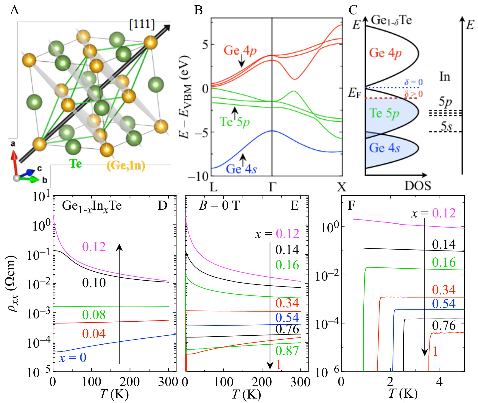 Figure 1
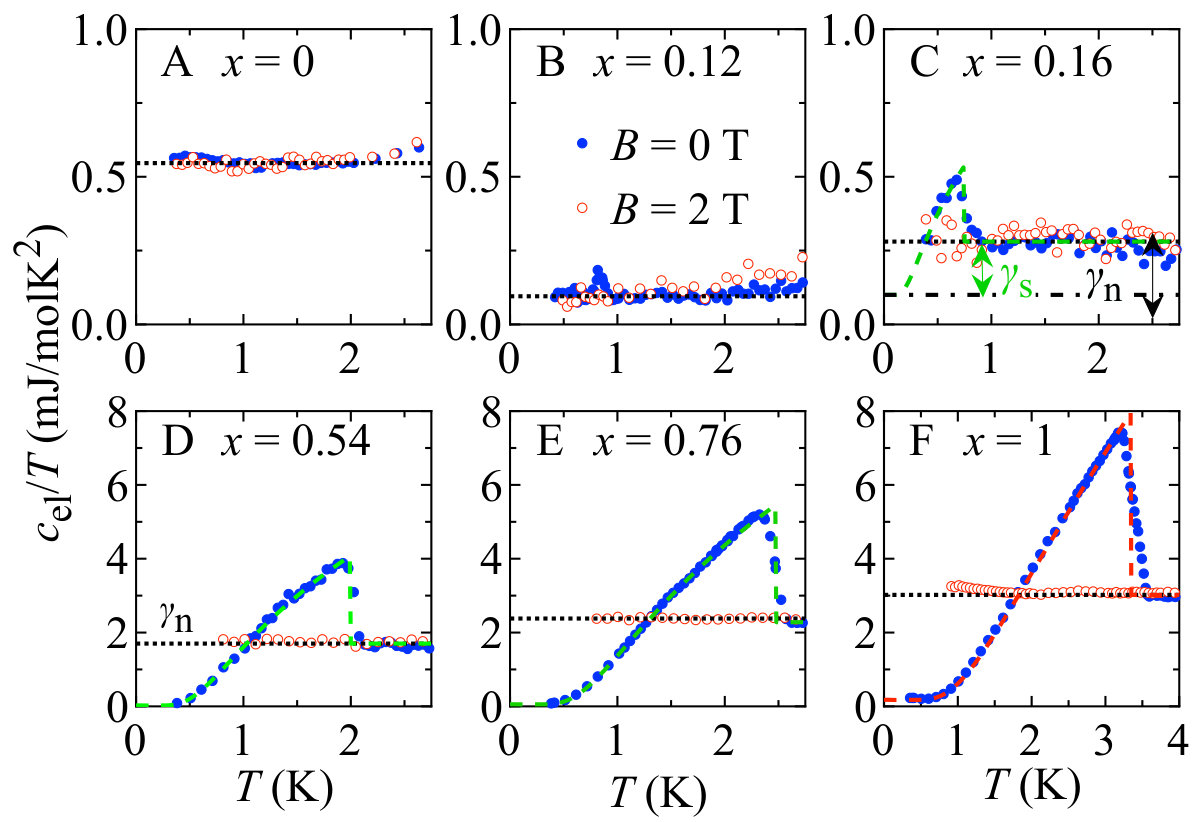 Figure 2
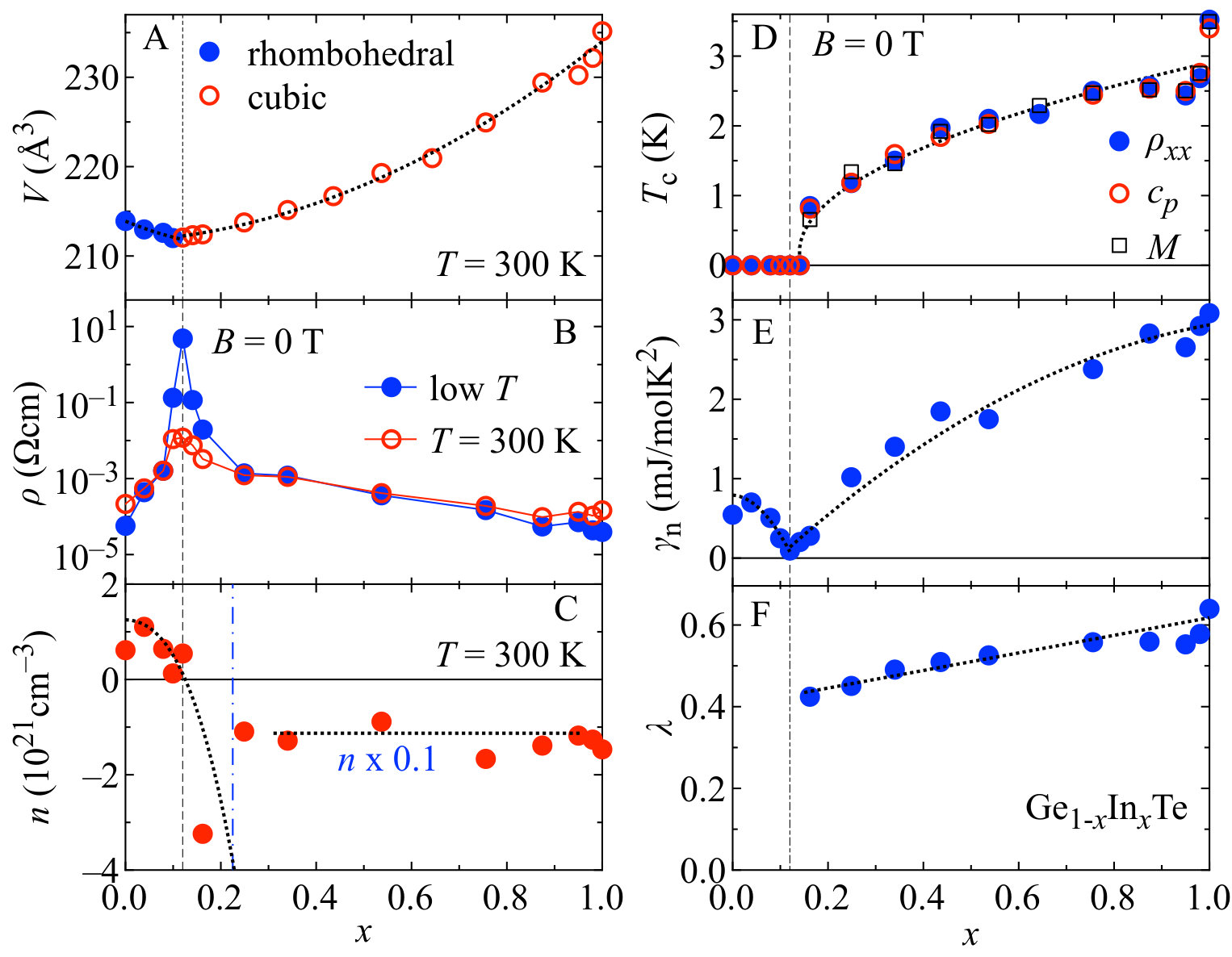 Figure 3
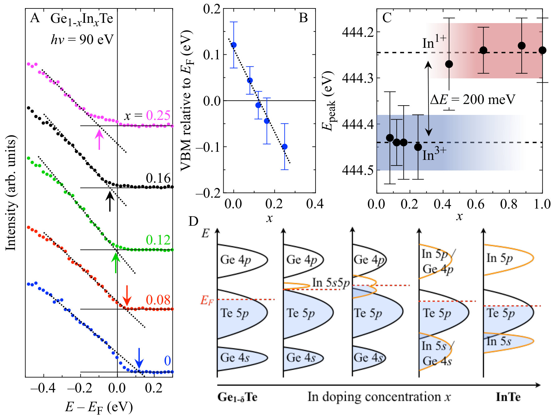 Figure 4
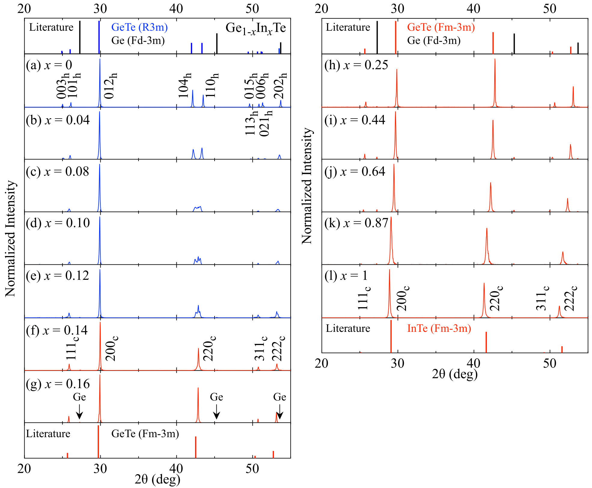 Figure 5
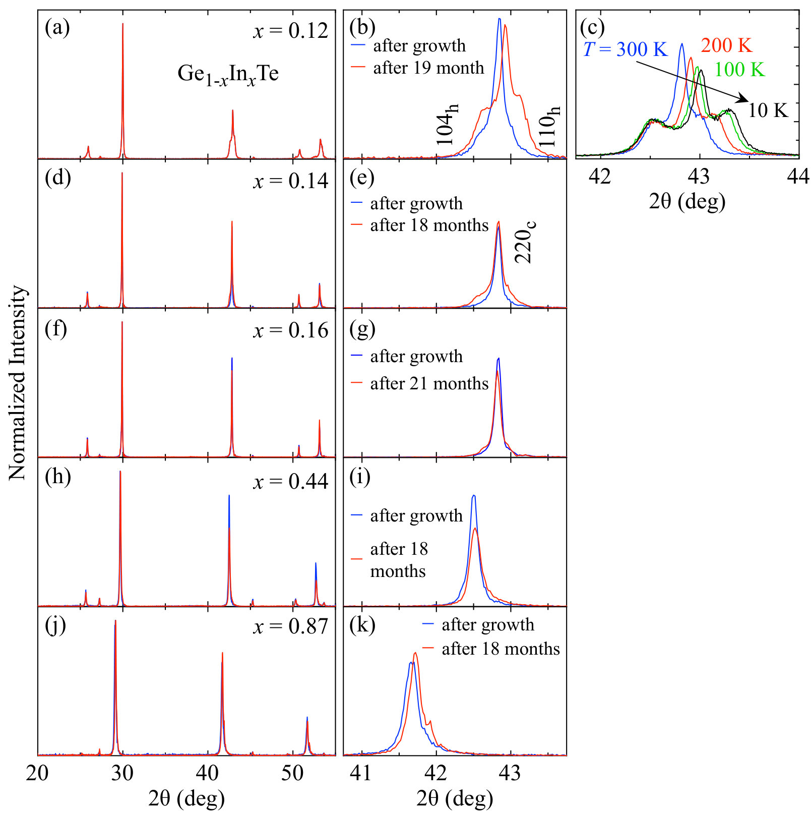 Figure 6
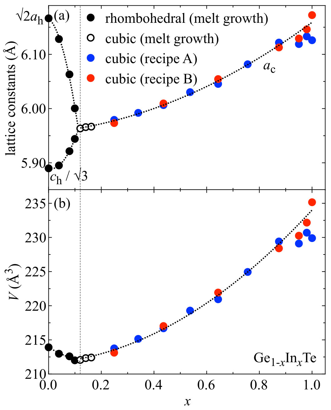 Figure 7
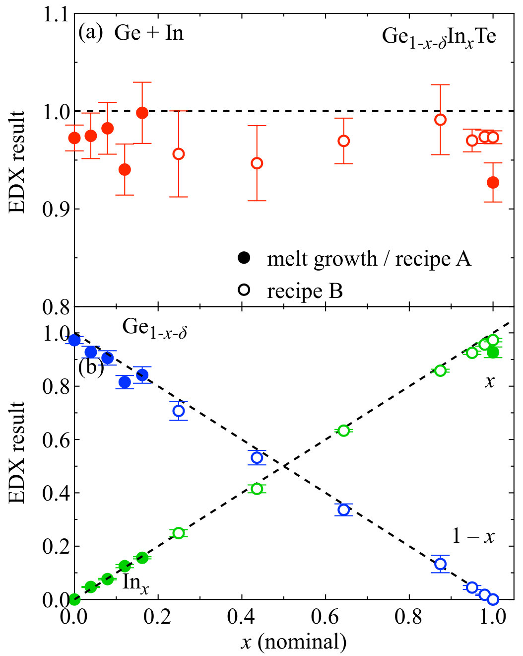 Figure 8
 Figure 9
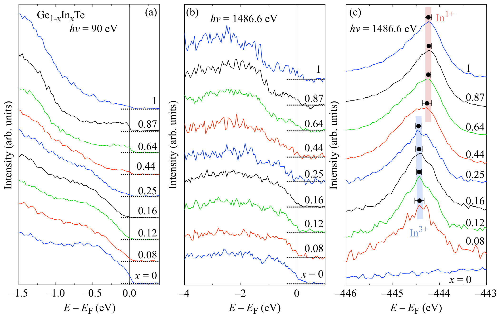 Figure 10
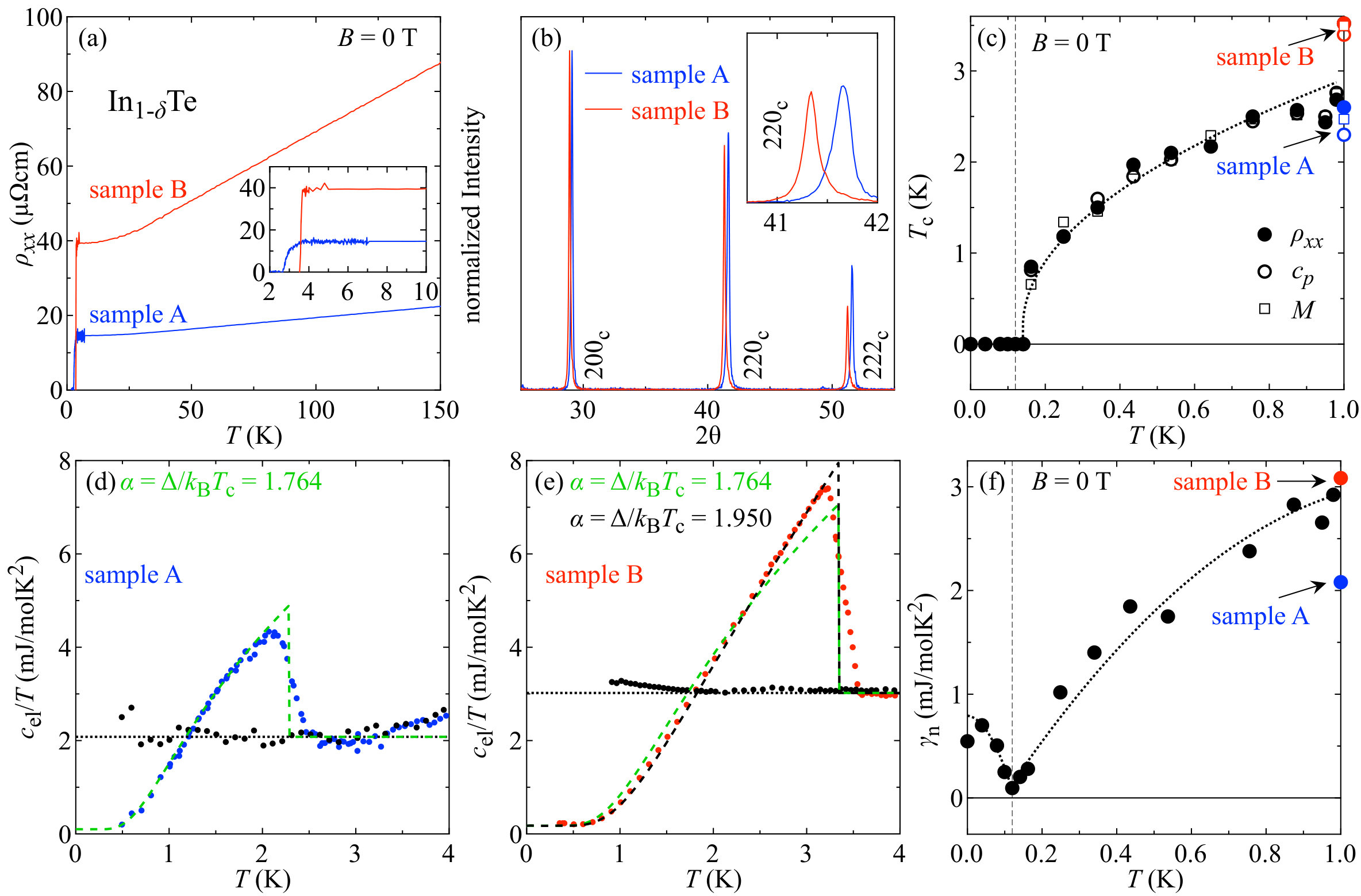 Figure 11
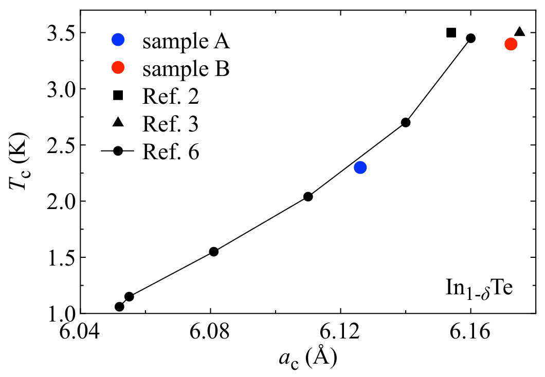 Figure 12
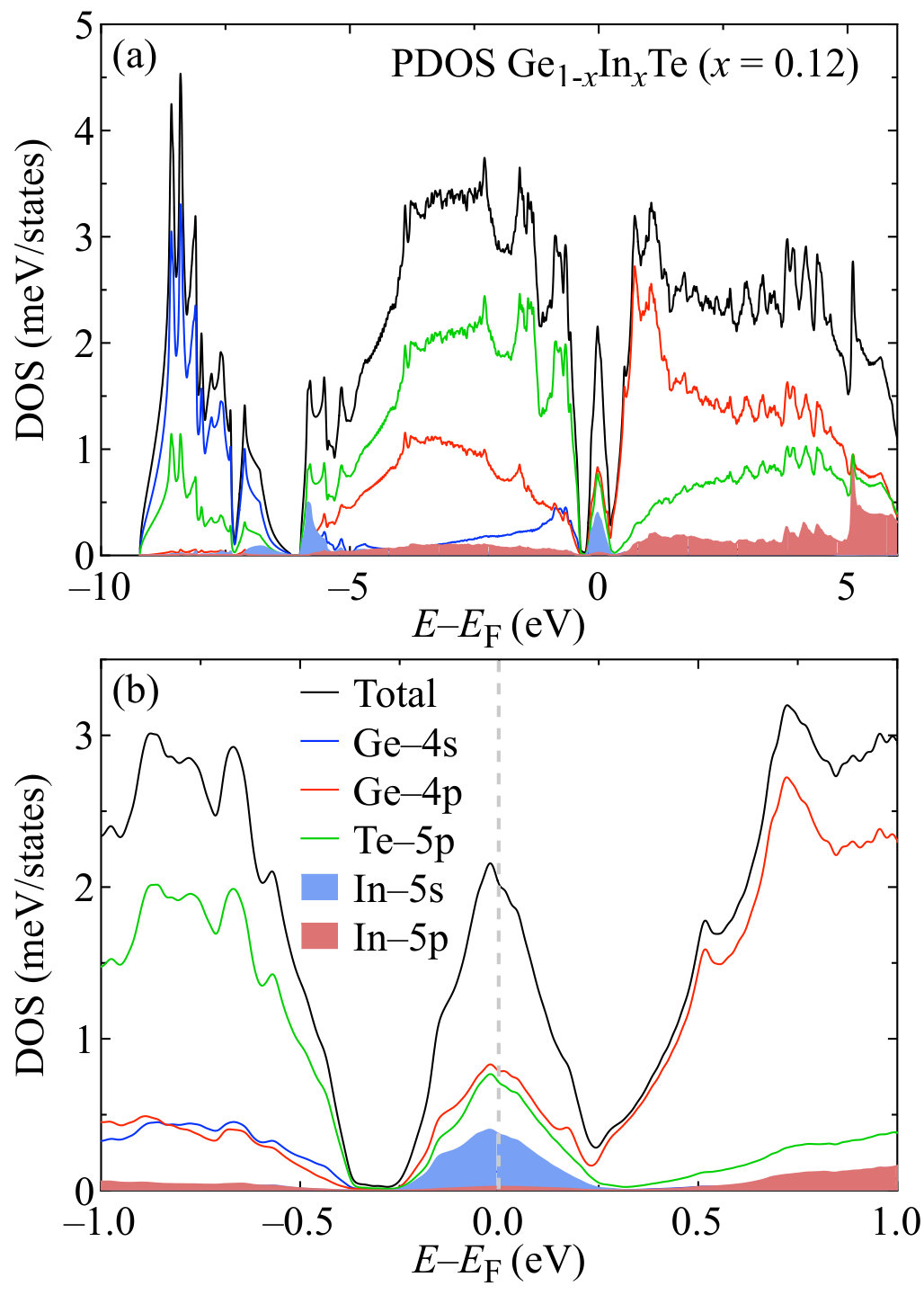 Figure 13
Peer Reviews
No public reviews on file for this paper yet. If you reviewed it on a platform where reviews are public (OpenReview, ICLR, NeurIPS, ICML), you can paste yours below so the community can read it here.
Videos
No videos yet. Explain this paper in a talk, walkthrough, or lecture? Add one.
Evolution of electronic states and emergence of superconductivity in the polar semiconductor GeTe by doping valence-skipping In
M. Kriener
RIKEN Center for Emergent Matter Science (CEMS), Wako 351-0198, Japan
M. Sakano
Department of Applied Physics and Quantum-Phase Electronics Center (QPEC), University of Tokyo, Tokyo 113-8656, Japan
M. Kamitani
RIKEN Center for Emergent Matter Science (CEMS), Wako 351-0198, Japan
M. S. Bahramy
RIKEN Center for Emergent Matter Science (CEMS), Wako 351-0198, Japan
Department of Applied Physics and Quantum-Phase Electronics Center (QPEC), University of Tokyo, Tokyo 113-8656, Japan
R. Yukawa
Photon Factory, Institute of Materials Structure Science, High Energy Accelerator Research Organization (KEK), Tsukuba, Ibaraki 305-0801, Japan
K. Horiba
Photon Factory, Institute of Materials Structure Science, High Energy Accelerator Research Organization (KEK), Tsukuba, Ibaraki 305-0801, Japan
H. Kumigashira
Photon Factory, Institute of Materials Structure Science, High Energy Accelerator Research Organization (KEK), Tsukuba, Ibaraki 305-0801, Japan
Institute of Multidisciplinary Research for Advanced Materials (IMRAM), Tohoku University, Sendai 980-8577, Japan
K. Ishizaka
RIKEN Center for Emergent Matter Science (CEMS), Wako 351-0198, Japan
Department of Applied Physics and Quantum-Phase Electronics Center (QPEC), University of Tokyo, Tokyo 113-8656, Japan
Y. Tokura
RIKEN Center for Emergent Matter Science (CEMS), Wako 351-0198, Japan
Department of Applied Physics and Quantum-Phase Electronics Center (QPEC), University of Tokyo, Tokyo 113-8656, Japan
Y. Taguchi
RIKEN Center for Emergent Matter Science (CEMS), Wako 351-0198, Japan
Abstract
GeTe is a chemically simple IV – VI semiconductor which bears a rich plethora of different physical properties induced by doping and external stimuli. These include, among others, ferromagnetism, ferroelectricity, phase-change memory functionality, and comparably large thermoelectric figure of merits. Here we report a superconductor - semiconductor - superconductor transition controlled by finely-tuned In doping. Our results moreover show the existence of a critical doping concentration around in Ge1-xInxTe, where various properties take either an extremum or change their characters: The structure changes from polarly-rhombohedral to cubic, the resistivity sharply increases by orders of magnitude, the type of charge carriers changes from holes to electrons, and the density of states diminishes at the dawn of an emerging superconducting phase. By core-level photoemission spectroscopy we find indications of a change in the In-valence state from In3+ to In1+ with increasing , suggesting that this system is a new promising playground to probe valence fluctuations and their possible impact on superconductivity.
Superconductivity emerges from a wide range of parent materials, including insulators and semiconductors. When charge carriers are doped by partial substitution of one element for another to form out a sufficiently large density of states (DOS) at the Fermi level, superconductivity is established, provided that an effective attractive interaction works among electrons via lattice vibrations. Therefore, choosing appropriate dopant atoms offers to influence the superconductivity through the formation of DOS at the Fermi level, the provision of the attractive interaction among electrons, and the frequency of lattice vibrations. Historically, it was in the early 1960s that Cohen theoretically predicted superconductivity in many-valley semiconductors and semimetals Cohen (1964) due to their peculiar band structure, such as GeTe, SnTe, and SrTiO3 Hein et al. (1964); Schooley et al. (1965); Hein and Meijer (1969), which was experimentally confirmed soon after. In particular, SnTe, which has recently regained much attention as a topological crystalline insulator Hsieh et al. (2012); Tanaka et al. (2012), exhibits superconductivity below critical temperatures of less than 300 mK. Interestingly, the superconducting transition temperature is strongly enhanced by In doping in its cubic structure Haldolaarachchige et al. (2016); Kobayashi et al. (2018); Kriener et al. (2018). To explain this enhancement, the valence-skipping nature Varma (1988); Dzero and Schmalian (2005); Hase et al. (2016) of the dopant atom In has been often discussed Haldolaarachchige et al. (2016); Kobayashi et al. (2018); Kriener et al. (2018); Hase et al. (2017) likewise Bi, Sn, and Tl. In should formally take its divalent state but is expected to form out instead In1+ and In3+ or a mixture of both. On the basis of the so-called “negative- mechanism” Varma (1988), the valence-skipping nature is predicted to possibly enhance the superconducting interaction as it is discussed for Tl-doped PbTe Matsushita et al. (2005), Ag-doped SnSe Ren et al. (2013); Wakita et al. (2017), and K-doped BaBiO3 Cava et al. (1988).
These interesting implications for superconductivity turned our attention to closely related GeTe, which exhibits a rich variety of different physical properties Boschker et al. (2017), such as structural phase change memory functionality Chen et al. (1986); Lencer et al. (2008); Liu et al. (2011) and its magnetic analogue Kriener et al. (2016, 2017), ferromagnetism, multiferrocity Cochrane et al. (1974); Fukuma et al. (2003); Tong et al. (2011); Przybylińska et al. (2014); Kriegner et al. (2016), and good thermoelectric properties Snyder and Toberer (2008); Levin et al. (2013); Davidow and Gelbstein (2013) owing to its multi-valley band structure Herman et al. (1968); Ciucivara et al. (2006). Recently, it has become well known for a large Rashba spin splitting of its bulk bands due to strong spin-orbit coupling and a polar distortion Sante et al. (2013); Picozzi (2014); Rinaldi et al. (2014); Krempaský et al. (2016), as depicted in Fig. 1a, taking place at about 700 K from cubic (; -GeTe) to rhombohedral (; -GeTe) accompanied with an elongation of the unit cell along the cubic [111] direction Goldak et al. (1966); Pawley et al. (1966). The band structure is shown in Figure 1b for cubic GeTe for the purpose of simplicity. We note that in the case of rhombohedral structure, it has qualitatively the same features, apart from the Rashba spin splitting. The valence band is mainly of Te character while the conduction band primarily consists of Ge . Figure 1c gives a schematic view of the DOS (left) and the approximate position of the atomic orbitals of the dopant In (right). In both panels the small-gap feature of semiconducting GeTe is apparent (the band gap is of the order of 200 meV at the point of the Brillouin zone). In reality, however, GeTe features a metallic-like resistivity and superconducts at low temperatures mK owing to unintentionally doped holes due to Ge deficiency (Ge1-δTe). Thus far, there have been only a few reports available about the evolution of thermoelectric properties and the structure in Ge1-xInxTe Woolley (1965); Abrikosov and Danilovadobryakova (1976); Wu et al. (2017).
In this paper we report the successful synthesis of the whole solid solution Ge1-xInxTe by employing a high-pressure synthesis method and the discovery of a doping-induced superconductor – semiconductor – superconductor transition by means of transport and specific-heat measurements. At low doping, the resistivity is enhanced by orders of magnitude while the rhombohedral distortion is suppressed. Around the system becomes cubic and a new bulk superconducting phase is established at slightly higher doping concentrations. The unit-cell volume shrinks below and starts to expand above with increasing . Coinciding with these transitions, the charge carriers change from hole to electron type. These observations imply that a change of the In-valence states from In3+ (electron doping) to In1+ (hole doping) may play a role. Core-level photoemission-spectroscopy data support such a scenario, where at higher doping additional features indeed appear, being indicative of the evolution of a different In-valence state. A model based on this valence-state change is proposed and can explain satisfactorily all observed features.
Results
The longitudinal resistivities of selected samples are summarized in Figs. 1d () and 1e (). As for the Ge1-δTe sample used here, we estimate % from the charge-carrier concentration at room temperature, giving rise to metallic conduction (: temperature). When doping In, the absolute values of the resistivity increase drastically and the shape of changes. While still exhibits a metallic-like dependence, this is not the case any more upon higher doping. Samples with exhibit a semiconductor-like dependence of the resistivity. The largest absolute value of in this study is found for , the data of which are shown in both panels (d) and (e) for clarity. As compared to , the resistivity at 2 K is enhanced by five orders of magnitude. Nevertheless the absolute value of is still of the order of a few cm and hence cannot be associated with a finite band gap. Upon further increasing , the resistivity becomes again smaller, and for all studied samples exhibit a metallic-like dependence of . Figure 1f provides an expanded view of the low- region below 5 K, revealing superconducting transitions as indicated by sharp drops of the data for . Moreover monotonously increases with .
Electronic specific-heat data of selected samples Ge1-xInxTe are displayed as vs plots in Fig. 2. For the details of the analyses, cf. Ref. Kriener et al. (2018). In agreement with the resistivity results, there is no anomaly visible in data for in the range mK (Fig. 2a). Doping In leads to a suppression of the normal-state electronic specific-heat coefficient , and hence the DOS at the Fermi level. The lowest value is found for a sample with (Fig. 2b) which is most insulating. As already seen in resistivity data, further doping establishes superconductivity in Ge1-xInxTe. For (Fig. 2c), there is a jump-like anomaly in specific-heat data on top of a residual DOS corresponding to a nonsuperconducting phase fraction. According to our analysis, approximately % of the sample volume superconducts. Upon further doping all samples are found to be bulk superconductors with vanishing or rather small residual DOSs. Moreover, the transitions are sharp, indicating a good sample quality. Up to , data can be well reproduced by weak-coupling BCS theory as shown in Fig. 2c – e with and representing the superconducting gap size. However, for it is necessary to increase the BCS coupling strength to 1.95 to yield a satisfactorily description, as shown in Fig. 2f. This apparent difference is discussed in Section S8 of the Supporting Information (SI, Sup ). As for the samples with , we note that there are drops to zero in resistivity data, but there is no accompanying specific-heat anomaly, indicating filamentary superconductivity.
Several physical quantities of Ge1-xInxTe are summarized in Fig. 3. The evolution of the unit-cell volume with is shown in Fig. 3a. As summarized in Section S1 of the SI Sup , there is a coexistence region with rhombohedral and cubic phase fractions, and the structure is better described in the rhombohedral -GeTe setting for (blue symbols in Fig. 3a) and in cubic -GeTe above (red open symbols). The most interesting feature here is that the unit-cell volume shrinks as long as the system is rhombohedrally distorted. By contrast, strongly increases in the cubic phase. Notably, the overall evolution does not obey Vegard’s law, and already above , the slope of starts to increase. The dependence of the corresponding lattice constants are shown in Fig. S3a of the SI Sup .
Absolute values of the resistivity at room temperature and at low (at 2 K for and above for larger ) are plotted against in Fig. 3b. The sharp and strong enhancement of around is most pronounced at low and still clearly recognized at 300 K, highlighting this critical In-doping concentration in Ge1-xInxTe.
In Fig. 3c the charge-carrier concentrations are plotted against as estimated from magnetic-field dependent Hall-effect measurements at room temperature, although deduced from may show some deviation from the real carrier concentration for metallic samples. The hole-type charge-carrier concentration is quickly suppressed when introducing In. The resulting charge-neutrality point is located around , i.e., the most insulating doping range. In spite of the semiconductor-like slope of for , the electron concentrations in these samples are already of the order of cm*-3* and hence the conduction regime is barely metallic. For , stays almost constant around cm*-3*. The cation deficiency , which may affect the carrier density, is examined by a scanning electron microscope equipped with an energy-dispersive x-ray (SEM-EDX) analyzer on selected samples as described in Section S5 of the SI Sup .
Superconducting values as estimated from resistivity, specific-heat, and magnetization data increase monotonously with and agree well with each other, see Fig. 3d. Interestingly, near InTe, increases very rapidly.
Figure 3e shows the evolution of with . The value of the measured GeTe sample has a smaller value than the sample for , probably due to the particular value of the Ge deficiency of the examined specimen. Upon increasing the In concentration, is reduced and almost zero but finite around as already suggested by the evolution of the charge-carrier concentration. For larger , increases monotonously.
The final panel Fig. 3f summarizes the electron-phonon coupling strength as estimated from our quantitative specific-heat analyses. It increases with almost constant slope over the superconducting doping range . Interestingly the strong enhancement of for only is neither clearly reflected in nor in , cf. also Section S8 in the SI Sup .
To obtain information on how the electronic structure changes upon In doping, we performed photoemission spectroscopy. Figure 4a shows the valence-band spectra for around the Fermi energy , which is indicated by a vertical solid line. The observed behavior is typical for a -type semiconducting system. Arrows indicate the valence-band maximum (VBM) energy relative to , defined as intersection point of both solid and dotted lines for each . The energy values of the VBM are replotted in Fig. 4b. Apparently the VBM shifts linearly with from above to below and coincides with at the critical In concentration , indicating the depletion of the charge carriers at, and their sign change across this doping level. At higher doping , the spectra change qualitatively from semiconducting to metallic as can be seen in Figs. S6a and b of the SI Sup . A step or edge at reflects the metallic character of these samples.
The bulk-sensitive x-ray PES measurements ( eV) for the In- core-level allowed us to obtain information about the valence state of In, cf. Fig. S6 of the SI Sup . In the intermediate region of , the core-level structure broadens, and the peak position changes suddenly around . The peak energies are replotted in Fig. 4c. These two values are associated with the two valence states of In. Dashed horizontal lines are guides for the energies of both features. They are separated by approximately 0.2 eV, similarly as the Sn2+ and Sn4+ peaks in Sn core-level spectra of AgSnSe2 Wakita et al. (2017) or Sn oxides Themlin et al. (1992). In the case of AgSnSe2, Sn2+ and Sn4+ peaks appear at the binding energies of and eV, respectively, thus indicating a separation of eV. In analogy with this behavior, we attribute the energetically shallower feature ( eV) to the In1+ and the deeper one ( eV) to the In3+ state.
Discussion
Apparently is a critical In concentration around which several properties of Ge1-xInxTe change dramatically. The structure changes from rhombohedral to cubic, the unit cell shrinks below and expands above, the resistivity is strongly enhanced by five orders of magnitude within a very small doping range around , the charge-carrier type changes from hole to electron, superconductivity emerges, and the DOS is depleted. Given that Ge1-δTe is a very-low- superconductor, the system apparently runs through a superconductor – semiconductor – superconductor transition. Also, as described in the introduction, the In dopant is a so-called valence-skipping element with favorable In1+ () and In3+ () valence states Varma (1988); Erickson et al. (2009); Hase et al. (2016). Therefore it is reasonable to think about their role in this system.
The sketch in Fig. 4d illustrates the plausible evolution of the In states as a function of the In concentration on the basis of the results summarized in Figs. 1 – 4. The left-most schematic DOS shows the situation in Ge1-δTe and is similar to that in Fig. 1c. The Fermi level (red dashed line) lies in the Te- band, giving rise to metallic-like conduction with a hole-type carrier concentration of the order of cm*-3*. The second schematic picture shows the situation for light In doping, which very effectively reduces the hole-type carriers, shifting the Fermi level upwards. From literature Haldolaarachchige et al. (2016) it is known that light In doping leads to the formation of impurity states located at the top of the VBM. This is also confirmed by our band calculation for (see Section S9 in the SI Sup ). In the sketch, this feature is labelled “In ” to emphasize its origin from the respective atomic In orbitals. These newly-formed states are mostly empty, and hence the valence state of In is 3+. Upon further doping, the impurity band becomes wider and the initial “In ” states start to separate as shown in the central schematic drawing of Fig. 4d, and the conduction mechanism will gain again metallic character above . The next schematic shows how the bands of In – Ge and In – Ge characters form mixed orbital states at higher doping, called “amalgamated bands” in Ref. Onodera and Toyozawa (1968). When the doping level is sufficiently high, the In- orbitals will have developed into a proper fully occupied band which has shifted below the Te- band and hence well below . Only the In- band remains empty, thus In now takes its 1+ state.
The analysis of the In- core-level photoemission spectra allows us to further confirm this: For low doping up to approximately , we can only identify the feature at higher binding energy (In3+). From a second feature develops, indicating that the valence state of the dopants start to become 1+. At the same time the peak indicative of the In3+ state fades away and is hardly seen for , cf. Fig. S6c of the SI Sup . Therefore the crossover from 3+ to 1+ mainly takes place in the intermediate In-doping range between and , cf. Fig. 4c. The change in the In valence states is also reflected in the nonmonotonous behavior of the unit-cell volume with , cf. Fig. 3a: decreases as increases to because of the smaller ionic radius of In3+, but tends to nonlinearly increase above due to the increasing fraction of In1+ ions with larger radius. At higher doping, the system behaves like a simple metal as also indicated by resistivity data shown in Fig. 1(e). This situation is sketched in the final drawing in Fig. 4d for pure InTe, where a metallic ground state with a large Fermi surface and empty In- bands is realized. To assume the 1+ state for In is reasonable even for metallic InTe (without ionic bonds), because of the energetic proximity of the Te and In states which allows for an easy charge transfer between them.
Finally we discuss some striking differences between In-doped SnTe and In-doped GeTe, given that both are isostructural and share qualitatively many similar features. Charge carriers originate from unintentionally self-doped holes leading to low-temperature superconductivity, which is depleted by doping In. However, when doping In as little as , Sn1-xInxTe becomes again superconducting with values of up to K Erickson et al. (2009); Novak et al. (2013). Since the suppression of the polar distortion requires In doping of , lower-doped Sn1-xInxTe is a polar superconductor. By contrast, in Ge1-xInxTe the doping-induced superconducting phase only emerges above the structural transition . While in Ge1-xInxTe the charge neutrality point and hence the change of the carrier type coincides with the structural transition and various other features, in Sn1-xInxTe the sign change of the carriers happens around Haldolaarachchige et al. (2016) which is higher than the concentration of the structural transition. Another significant difference is the dependence of : Sn1-xInxTe features a two-dome phase diagram with a strong and sudden suppression of around Kriener et al. (2018). By contrast, monotonously increases with in Ge1-xInxTe, as shown in Fig. 3d. This might be a consequence of the difference in the respective ionic radii and atomic energy levels between Ge and Sn, giving rise to distinct degrees of local lattice distortion and hybridization with the In and Te states. However, the band inversion apparent in SnTe, which was reported to survive at least light In doping Tanaka et al. (2012); Sato et al. (2013), may further complicate the situation. To chase down the origins of these pronounced differences between the two systems Ge1-xInxTe and Sn1-xInxTe that are at first glance very similar, and to answer the question about the exact role of the valence state of In are promising starting points for future studies.
Acknowledgments
This work was partly supported by Grants-In-Aid for Scientific Research (S) from the Japan Society for the Promotion of Science (JSPS, No. 24224009), JST (No. JP16H00924), and PRESTO (JPMJPR15N5) and Grants-In-Aid for Scientific Research (B) (JSPS, No. 17H02770). MK is supported by a Grants-in-Aid for Scientific Research (C) (JSPS, No. 15K05140). We thank R. Arita and T. Koretsune for fruitful discussions.
The reference list from the paper itself. Each links out to its DOI / PubMed record.
- 1Cohen (1964) M. Cohen, Phys. Rev. 134 , A 511 (1964).
- 2Hein et al. (1964) R. Hein, J. Gibson, R. Mazelsky, R. Miller, and J. Hulm, Phys. Rev. Lett. 12 , 320 (1964).
- 3Schooley et al. (1965) J. Schooley, W. Hosler, E. Ambler, J. Becker, M. Cohen, and C. Koonce, Phys. Rev. Lett. 14 , 305 (1965).
- 4Hein and Meijer (1969) R. A. Hein and P. H. E. Meijer, Phys. Rev. 179 , 497 (1969).
- 5Hsieh et al. (2012) T. H. Hsieh, H. Lin, J. Liu, W. Duan, A. Bansil, and L.Fu, Nat. Commun. 3 , 982 (2012).
- 6Tanaka et al. (2012) Y. Tanaka, Z. Ren, T. Sato, K. Nakayama, S. Souma, T. Takahashi, K. Segawa, and Y. Ando, Nature Phys. 8 , 800 (2012).
- 7Haldolaarachchige et al. (2016) N. Haldolaarachchige, Q. Gibson, W. Xie, M. B. Nielsen, S. Kushwaha, and R. J. Cava, Phys. Rev. B 93 , 024520 (2016).
- 8Kobayashi et al. (2018) K. Kobayashi, Y. Ai, H. O. Jeschke, and J. Akimitsu, Phys. Rev. B 97 , 104511 (2018).