Two-dimensional electron gas in a metal/amorphous oxide interface with spin orbit interaction
Jose Manuel Flores-Camacho, Jorge Puebla, Florent Auvray, Alfonso, Lastras-Martinez, Yoshichika Otani, Raul Eduardo Balderas-Navarro

TL;DR
This study uses infrared spectroscopic ellipsometry to confirm the formation of a spin-orbit coupled two-dimensional electron gas at a metal/amorphous oxide interface, revealing its properties and hybridization effects.
Contribution
It demonstrates the detection and characterization of 2DEG with SOC in amorphous materials, overcoming previous experimental challenges.
Findings
Confirmed 2DEG formation at Cu/Bi₂O₃ interface
Identified signatures of SOC in optical response
Validated theoretical predictions of 2DEG behavior
Abstract
The formation of novel two-dimensional electron gas (2DEG) with high mobility in metal/amorphous interfaces has motivated an ongoing debate regarding the formation and novel characteristics of these 2DEGs. Here we report an optical study, based on infrared spectroscopic ellipsometry, of nonmagnetic metal and amorphous semiconducting oxide (Cu/BiO) interfaces that confirms the formation of a 2DEG with spin orbit coupling (SOC). The 2DEG optical response was simulated with a uniaxial diagonal dielectric tensor within a sub-nanometer thin layer, where its and components lineshapes resolved in both free-electron and peak-like contributions, resulted very similar to theoretical predictions [M. Xie et al., Phys. Rev. B , 245417 (2014)] of a two dimensional electron gas confined in the normal direction of a perovskite interface. In particular, the small but finite…
Click any figure to enlarge with its caption.
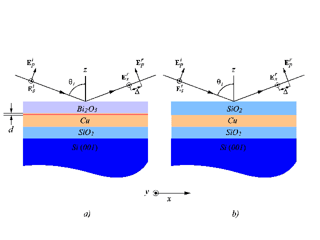 Figure 1
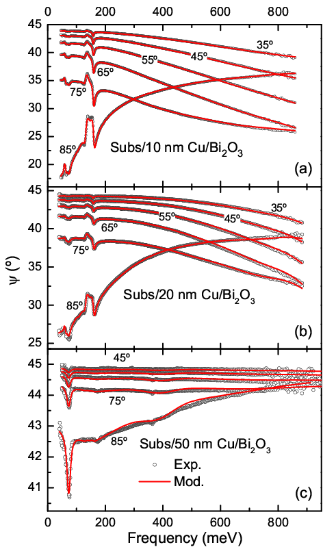 Figure 2
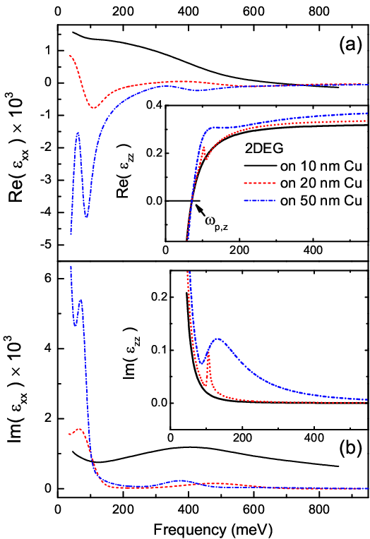 Figure 3
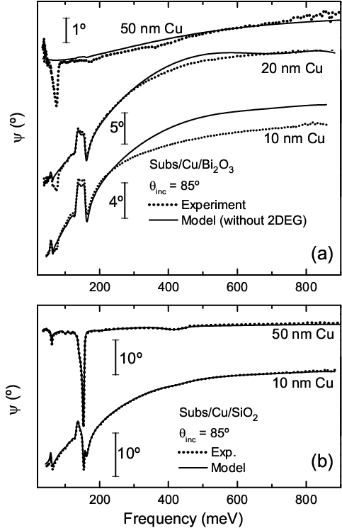 Figure 3
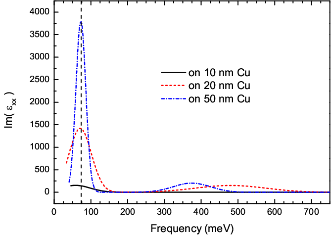 Figure 4
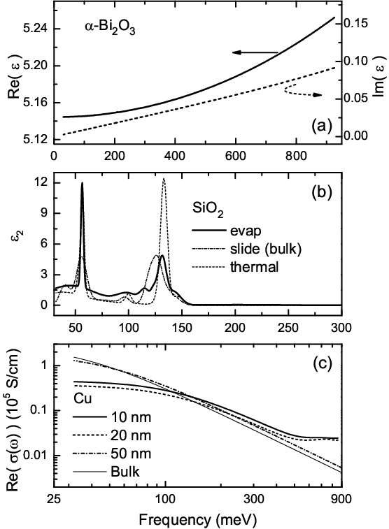 Figure 5
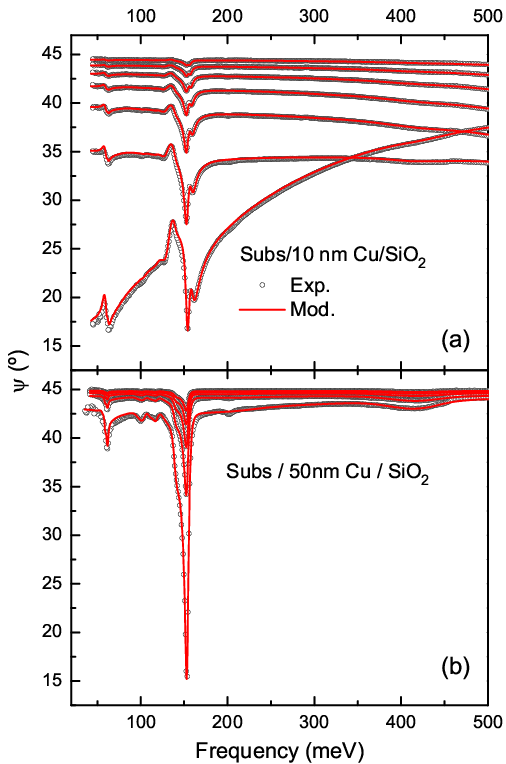 Figure 6
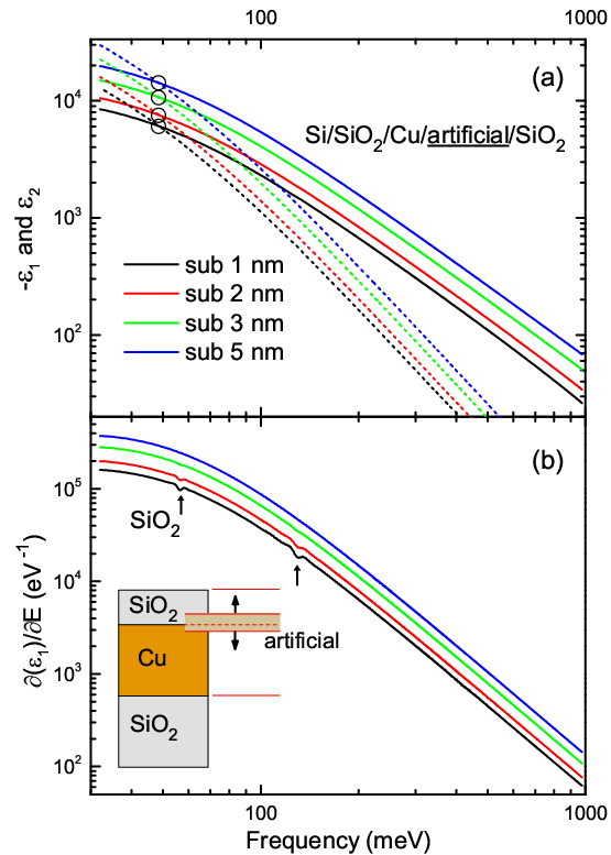 Figure 7
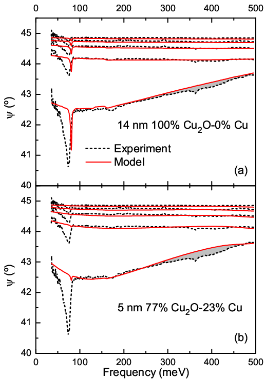 Figure 8
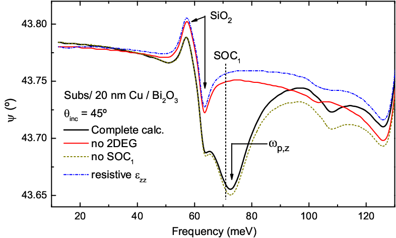 Figure 9
| Free-electron | SOC1 | SOC2 | |||||||
|---|---|---|---|---|---|---|---|---|---|
| (nm) | (nm) | S/cm) | (fs) | (S/cm) | (fs) | (meV) | (meV) | (meV) | (meV) |
| 10 | – | – | |||||||
| 20 | |||||||||
| 50 | |||||||||
Peer Reviews
No public reviews on file for this paper yet. If you reviewed it on a platform where reviews are public (OpenReview, ICLR, NeurIPS, ICML), you can paste yours below so the community can read it here.
Videos
No videos yet. Explain this paper in a talk, walkthrough, or lecture? Add one.
Two-dimensional electron gas in a metal/amorphous oxide interface with
spin orbit interaction
Jose Manuel Flores-Camacho
Instituto de Investigación en Comunicación Óptica, Universidad Autónoma de San Luis Potosí, Álvaro Obregón 64, 78000 San Luis Potosi, Mexico
Jorge Puebla
Center for Emergent Matter Science, RIKEN, Wako, Saitama 351-0198, Japan
Florent Auvray
Center for Emergent Matter Science, RIKEN, Wako, Saitama 351-0198, Japan
Institute for Solid State Physics, University of Tokio, Kashiwa, Chiba 277-8581, Japan
Alfonso Lastras-Martínez
Instituto de Investigación en Comunicación Óptica, Universidad Autónoma de San Luis Potosí, Álvaro Obregón 64, 78000 San Luis Potosi, Mexico
Yoshichika Otani
Center for Emergent Matter Science, RIKEN, Wako, Saitama 351-0198, Japan
Institute for Solid State Physics, University of Tokio, Kashiwa, Chiba 277-8581, Japan
Raul Eduardo Balderas-Navarro
Instituto de Investigación en Comunicación Óptica, Universidad Autónoma de San Luis Potosí, Álvaro Obregón 64, 78000 San Luis Potosi, Mexico
Abstract
The formation of novel two-dimensional electron gas (2DEG) with high mobility in metal/amorphous interfaces has motivated an ongoing debate regarding the formation and novel characteristics of these 2DEGs. Here we report an optical study, based on infrared spectroscopic ellipsometry, of nonmagnetic metal and amorphous semiconducting oxide (Cu/Bi2O3) interfaces that confirms the formation of a 2DEG with spin orbit coupling (SOC). The 2DEG optical response was simulated with a uniaxial diagonal dielectric tensor within a sub-nanometer thin layer, where its and components lineshapes resolved in both free-electron and peak-like contributions, resulted very similar to theoretical predictions [M. Xie et al., Phys. Rev. B 89, 245417 (2014)] of a two dimensional electron gas confined in the normal direction of a perovskite interface. In particular, the small but finite conducting character of the component provides a unambiguous signature of the presence of the 2DEG in the Cu/Bi2O3 system. Although the original constituent materials do not possess spin-orbit coupling (SOC), the resulting interfacial hybridization of such states induce electronic asymmetric wave functions. This work demonstrates the detection of 2DEG in amorphous crystals allowing to study its challenging interfacial phenomena such as SOC and interface-bulk coupling, overcoming an experimental impediment which has hold back for decades important advancements for the understanding of 2DEGs in amorphous materials.
pacs:
78.68.+m, 73.20.-r, 73.40.-c, 71.70.Ej
††preprint: preprint
I Introduction
The concept of two-dimensional electron gas (2DEG) has contributed enormously to the understanding of the rich phenomena of electrons confined at surfaces and interfaces. In high quality semiconductor heterostructures, 2DEG confinement induced enhancement of electron mobility leading to technology advancements and scientific discoveries, such as the fractional Quantum Hall effect Stormer et al. (1999). The continuous development of growth techniques allows nowadays to obtain enough good quality heterostructures from oxides, forming novel 2DEGs. Interestingly, 2DEG in oxides show a significant increase in electron density and strong electron correlation, with consequences in magnetic properties, superconductivity, ferroelectricity and spin orbit interaction Mannhart and Schlom (2010); Hwang et al. (2012). Intrinsically, the electronic structure of 2DEG in oxide interfaces is different from the most standard semiconductor counterparts. In most of the oxide interfaces, the transport properties are dominated by narrow -band electrons, whereas in semiconductors the electrons localized at states at the bottom of the conduction band dictate the properties of the 2DEGs. However, despite of the great advance in the understanding of 2DEG in complex oxide interfaces, still many oxide interfaces are challenging to characterize, mainly because their crystal quality. Analysis of the electronic structure is commonly achieved by angle-resolved photoemission spectroscopy (ARPES). However, ARPES characterization requires high quality, large and flat crystals. For instance, high quality crystals of bismuthates were obtained, allowing detailed characterization by ARPES and reveling the mechanism of its high temperature superconductivity, an open discussion for more than 30 years Wen et al. (2018).
Moreover, the formation of novel 2DEG with high mobility in amorphous oxides has motivated an increasing interest Lee et al. (2012); Chen et al. (2015). The origin of the 2DEG formation at these interfaces has been assigned to electronic reconstruction via interfacial charge transfer Liu et al. (2013); however, detailed characterization of the properties of 2DEGs formed by amorphous oxides is still lacking. An alternative to ARPES characterization is to analyze the optical conductivity of the 2DEGs by polarized spectroscopy techniques such as spectroscopic ellipsometry. Although, structural distortion and defects in amorphous materials may cause complex dielectric screening, and significantly complicate the analysis of the properties of the 2DEG, a theoretical model can be assessed and improved by direct feedback from optical characterization Xie et al. (2014).
Here, we report on mid-infrared ellipsometry characterization of the properties of 2DEG formed at the interface between a nonmagnetic metal and amorphous semiconducting oxide, Cu/Bi2O3. Recent spin-charge interconversion experiments suggest the presence of a 2DEG with spin orbit coupling (SOC) at this interface Puebla et al. (2017); Xu et al. (2018); Tsai et al. (2018), making it a very attractive structure for spin based complementary metal-oxide semiconductor technologies (CMOS) Manipatruni et al. (2018, 2019). The characterization by angle resolved ellipsometry confirms the formation of a 2DEG with SOC. In-depth analysis of the optical conductivity, modeled by a realistic electronic structure system and Kubo formalism, allows to define the origin of SOC as the hybridization of interfacial Cu-O-Bi states by charge transfer, generating an asymmetric wave function Tsai et al. (2018), as previously suggested for amorphous perovskite oxides Chen et al. (2015); Liu et al. (2013).
The rest of the paper is organized as follows. The main and reference samples are described in Sec. II together with a brief description of the ellipsometry technique. In Sec. III we present the dielectric functions of the stacked system and the model for the tensorial dielectric function of the 2DEG forming at the Cu/Bi2O3 interface. Finally, results and discussion are given in Sec. IV.
II Experiment
The samples consist of Bi2O3 films, with thickness of 20 nm, grown on a previously (either 10, 20, or 50 nm thick) Cu-capped SiO2/Si(001) substrate as described elsewhere Puebla et al. (2017); Auvray et al. (2018). The structure is shown in Fig. 1(a). Additionally, in order to contrast the presence of 2DEG and for obtaining the dielectric function (DF) of thin Cu film alone, a second set of reference samples were prepared as shown in Fig. 1(b). Two other samples, Si/SiO2 and Si/SiO2/Bi2O3 were made in order to measure the SiO2 film thickness of all samples’ common substrate, and to determine the dielectric function of Bi2O3 in the present spectral range.
The samples were characterized by infrared spectroscopic ellipsometry (IRSE) by means of an IR-VASE apparatus (J.A. Woollam Co.). Ellipsometry measures the change in polarization state upon oblique reflection of an originally linear polarized incident beam Azzam and Bashara (1977). The reflected state of polarization is measured by the complex ratio
[TABLE]
where and are the complex reflection coefficients for and polarizations of light, standing for parallel and perpendicular to the plane of incidence, respectively. The ellipsometric angles and measure then the relative change of amplitude and phase, respectively, of the to polarizations Humlíček (2005). Mid-infrared SE (spectroscopic ellipsometry) was measured in the range of 35 to 760 meV in ambient conditions for angles of incidence . As the indicatrix of an uniaxial material is oriented with its distinct axis perpendicular to the sample surface, i.e., an ordinary so-called isotropic-like ellipsometry measurement is sufficient to fully characterize the optical properties Fujiwara (2007). Neither off-diagonal Jones matrix elements nor Müller matrix measurements provided further information for our samples.
For the mid-infrared studies, where silicon is transparent, partially incoherent light reflected off the backside surface can reach the detector. Thus the backside of the samples were subjected to a sand-blasting treatment, obtaining thus a surface rough enough so as to avoid specular, spurious reflection from it. The success of the treatment is tested by transmission and depolarization measurements, which are acquired with the same ellipsometer. Transmission turned out to be negligible for all samples, whereas the loss of polarization yielded near zero values as well, except for samples with thicker Cu film and only for , for which the loss is below 2.5%. This may indicate another source of depolarization. Resulting experimental spectra are shown with symbols in Fig. 2.
III Ellipsometry Model
In this section we describe the procedure to obtain the model employed in the present work for the diagonal, uniaxial, dielectric tensor representing the optical response of the 2DEG. We present first the model of stacked layers and the dielectric functions of the corresponding constituent materials followed by the 2DEG dielectric tensor. The model the 2DEG layer is stripped to the minimum number of oscillators that permitted a good fit. We note that the core result of this work, shown in Fig. 2, presents some deviations from experiment which might have been corrected by including more oscillators, however, this is avoided if a physical interpretation cannot be provided.
The layer basic constituents’ dielectric functions, i.e., those of Si, SiO2, the thickness dependent Cu, and Bi2O3, were obtained either from literature or extracted from reference samples, so that for the main Cu/Bi2O3 samples, the only permitted unknown is the 2DEG response. Moreover, spectra corresponding to all angles of incidence are fitted together employing the same constituents. This ensures consistency of the model.
III.1 Constituent materials
The total reflection coefficients Heavens (1995) in Eq. (1) are calculated separately for and polarizations using Fresnel coefficients consisting of, for the main Cu/Bi2O3 samples, a model of 6 stacked media: (0) vacuum, (1) 20 nm Bi2O3, (2) an interfacial, anisotropic layer to accommodate the 2DEG, (3) Cu thin film, (4) 320 nm SiO2, and (5) Si substrate [see Fig. 1(a)]. Similar models are used for the different reference samples, for instance, Fig. 1(b) corresponds to Si/SiO2/Cu/SiO2. It is important to note that attempts made to model the Cu/Bi2O3 spectra without the artificially introduced 2DEG layer failed to simulate the main features of the experimental curves as presented in Fig. 3(a). However, it worked nicely for the Cu/SiO2 reference samples, as shown in Fig. 3(b), indicating that the interfacial layer must be necessarily included in the description of the optical response of the Cu/Bi2O3 system.
In order to ensure Kramers-Kronig consistency, the complex dielectric function of each layer is parameterized as a sum of oscillators of a general form
[TABLE]
where is a (real) constant offset, the terms are used to include resonances within the measured spectral range, commonly Lorentz or complex Gaussian functions. is the Tauc-Lorentz oscillator Jellison (2005), which is used here because of its pulse-like shape as described below. The term corresponds to the classical Drude model for free carriers expressed through
[TABLE]
where the offset with which this equation is commonly written is passed to in Eq. (2), and is the DC conductivity, which, for the case of the interfacial 2DEG, will be replaced by the appropriate tensorial component . Similarly, in this layer the characteristic life time will be direction dependent, as well. However, if the material of the layer is around the percolation threshold, the Drude term can be replaced by a Drude-Smith line shape given by Smith (2001)
[TABLE]
which accounts for stochastic persistency of velocity of carriers after scattering events measured through the factor (). In this model will be the average collision time, and thus the real DC conductivity, i.e., the one obtained by extrapolation to is reduced with respect to that of the pristine material. The Drude-Smith model predicts a shift of spectral weight which is expressed by a broad peak in the mid-infrared region Smith (2001) in agreement with classical percolation theories Stroud (1979). The required Lorentzian and Tauc-Lorentz oscillators are only phenomenological descriptions for the physical reality of the spin-orbit coupling Xie et al. (2014) related bands and inter-subband transitions that serve to place experimentally those resonances.
The dielectric function of -Bi2O3 was extracted from a Si/thermal SiO2/Bi2O3 reference sample. To this end a reference substrate Si/SiO2 was fitted first. The thermal SiO2 dielectric function was taken from data sets without modifications. It is shown in Fig. 4(b) (dashed line). The resulting complex dielectric function of Bi2O3 is shown in Fig. 4(a).
Employment of Si/SiO2/Cu/SiO2 reference samples was required to extract the thickness dependent Cu dielectric function, since in this samples no 2DEG formation is expected. Due to the preparation method, i.e., evaporation instead of thermal formation, the dielectric function of the most external SiO2 layer did require some modification. Its resembles more that of a bulk glass (a microscope slide). In Fig. 4(b) we show the spectral region where the preparation-dependent differences are stronger Kitamura et al. (2007).
For the present Cu thin layers, the bulk dielectric function cannot be used since for these thicknesses the Cu layers are still near the mentioned percolation threshold Hövel et al. (2010); Lee et al. (2011); Amotchkina et al. (11) even though they are already continuous. The layers of 20 and 50 nm required the classical Drude model only, however, for the 10 nm Cu film the Drude-Smith correction was necessary to better fit the Cu/SiO2 data of Fig. 3(a), since the model without the correction had the tendency of rising above the experimental data at the lower end of the spectrum. The resulting Cu optical conductivities are shown in Fig. 4(c), where bulk data Palik (1985) are shown for comparison.
III.2 Anisotropic model for the 2DEG
The 2DEG layer has drastically different transport properties along the Cu/Bi2O3 interface and perpendicular to it. This strong disparity prompted us to pursue a simulation-to-experiment approach instead of the common experiment-to-theory procedure. To extract its frequency dependent tensorial complex components and , we first proceeded with the assumptions that the conductivity along the interface is much greater than that of the out-of-plane component, and that a forced isotropic approximation could suffice to provide a preliminar lineshape as a first approximation, and thus, learn already something about the main spectral features as described next. A similar anisotropic approach has been conducted for perovskites characterized also by infrared ellipsometry Yazdi-Rizi et al. (2016) in which a Berreman resonance is excited by the presence of a longitudinal phonon in one of their constituents. In our case, on the other hand, the properties of the out-of-plane conductivity, in particular a sort of “bulk” plasmon-like characteristic frequency, and not a longitudinal phonon, are critical for the description of the present experiments as discussed in the following.
The extracted “isotropic” optical properties are to be considered a pseudo dielectric function of the layer: from a set of pre-simulations we first inferred that (the modulus of a tensor along a given direction) even for bulk-like transparent well-oriented uniaxial media, where and are direction cosines of the traveling electric displacement vector . This implies that, as we learned from simulations, in the case of free electron behavior described by Drude line shape of the form , where is the dc resistivity and is the characteristic time of life, that when the dc parts of the optical conductivity moduli follow the relation the isotropically forced conductivity tends to overestimate the dc component even by an order of magnitude. However, the isotropic-like time of life turns out to be along the interface, and tends to be always correctly predicted at least under the aforementioned dc conductivities relation. Interestingly, the bulk plasmon frequency ; i.e., the crossing Re, produces a resonant-like feature in ellipsometry spectra where there is no actual resonance. In fact, for the isotropic forced simulation, this peak was simulated with a Fano resonance due to its asymmetric form Fano (1961); Luk’yanchuk et al. (2010), which can be seen more clearly in the experimental spectrum at in Fig. 2(c), and was even seriously considered as a candidate to be a contribution of either or were not for the simpler explanation provided by the out-of-plane conductivity. Moreover, attempts to introduce a Fano resonance resulted in non physically negative dielectric functions. Therefore, any simulation taking into account Fano resonances was excluded in the anisotropic model. The asymmetric negative peak was thus obtained in simulations as follows: the feature is quite pronounced in calculated spectra of bulk-like samples if any one of and/or has this crossing, but for films on Cu substrates this apparent resonant feature is only revealed in calculated ellipsometry spectra for the crossing and not for even if this last function has it. We can therefore regard the presence of this feature, as the one at around 70 - 80 meV in Fig. 2, as a signature of the formation of an anisotropic layer at the Cu/Bi2O3 interface, which in our case is extremely revealing since our samples are composed of amorphous materials and therefore have isotropic dielectric functions. To sustain this proposition we note that () this is not a SiO2 vibration: the frequencies do not exactly correspond and for the sample with thicker Cu layer, as seen in Fig. 2(c), Cu clearly quenches any SiO2 feature, but the crossing related peak is very dominant. () This feature should not be confused with a Berreman peak Berreman (1963) or other similar peak-like features, since those occur either close to actual resonances Berreman (1963), when the substrate has a crossing Nucara et al. (2018) Re with positive slope (and not Re, as in our case), or when the real part of the dielectric functions at both sides of the interface coincide Park and Millis (2013); Dubroka et al. (2010), respectively. We clearly have not the conditions to fulfill any of these criteria.
For Lorentz or Gaussian line shapes, as the ones assigned to spin-orbit coupling bands in the next section, simulations showed that both characteristic centers and broadenings can be already correctly inferred from isotropic-like simulations. The real parts (Re)x and (Re)z, which describe the elastic response of the media, are inverted with respect to each other. For layered media, the real and imaginary parts seem to be interchanged in the total ellipsometry spectra. All these criteria provide guidance to decide whether a feature is to be part of the or component of the tensor, based also on reduction of fitting error.
Concerning film thicknesses, the forced isotropic “best” fit also overestimates film thicknesses of the supposed 2DEG layer. The obtained artificial layer thickness forming between Cu and Bi2O3 resulted in 2 to 3.6 nm depending on the underlying Cu film thickness for the forced-isotropic model, whereas for the more realistic uniaxial model, the thicknesses are all between 0.5 and 1 nm (see Table. 1, below).
Finally, for the 2DEG optical properties we propose the following description: the two-dimensional character of the electron gas will be described through a very thin layer with dielectric function of tensorial, uniaxial character, for which the carrier transport is much easier along the interface. The in-plane tensor modulus will have a Drude (or Drude-Smith) component to accommodate the free electron contribution to the 2DEG, and two Gaussian oscillators to simulate the SOC contributions Xie et al. (2014). The out-of-plane modulus will be comprised of a free electron Drude contribution, for which the relation holds, but which is nevertheless finite in such a way that it has a “bulk” plasmon Re crossing, which is critical in our model. Additionally, includes a Tauc-Lorentz oscillator whose role, expected by theoretical considerations Xie et al. (2014), will be described in the next section. The model as such is simple as desired, and quite descriptive of the actual experiments as seen in Fig. 2. Each spectral feature is modeled with two (for the classical Drude) to four parameters (for the percolation modified Drude-Smith model), which apparently amount to a large number of free quantities to determined, however, most of the spectral features are well separated from the rest and can be thus considered as independent from the others. Furthermore, the isotropic-forced first approach already provides a good estimation of the values some of them, specifically, the in-plane free-electron life time and positions of both SOC peaks. Additionally, the correlation between some parameters, and its possible source, is discussed at the end of the main text.
IV Results and discussion
The substrate Si/SiO2, and the Si/SiO2/Bi2O3 reference samples were fitted with VASE32, obtaining thus the thickness of the thermally grown SiO2 of 322 nm, and the mid-infrared pristine Bi2O3 dielectric function of Fig. 4(a), which are used for all subsequent samples. -Bi2O3 has a series of small phonons in this spectral region below 66 meV Narang et al. (1994); Kuzmenko et al. (1996), which were not detected in our experiment. Also, the group of features at and meV in Fig. 2(a), (b), and Fig. 3(a),(b) correspond to SiO2 and their strengths, when SiO2 is used only as the substrate of Cu/Bi2O3, can therefore be employed as a gauge of spectral absorption by the different Cu layers. For the SiO2/Cu/SiO2 reference spectra, shown in Fig. 3, the dips are easily reproduced by the proper model without great effort.
Experimental and calculated spectra for the different Cu/Bi2O3 samples recorded at several angles of incidence are shown in Fig. 2(a)-(c). The overall spectra are dominated by Cu reflectivity and its corresponding thickness-dependent optical conductivity . The resulting tensorial dielectric complex moduli, and of the 2DEG forming at the Cu/Bi2O3 interface are presented in Fig. 5. The resulting dielectric properties depend on the underlying Cu film thickness-driven transport properties. This dependence can be explained in terms of modulation of charge transfer from Cu to Bi2O3 due to the mobility of electrons within the Cu layer itself: for thicknesses below 20 nm the layer is below its percolation threshold (in fact, 10 nm Cu was modeled with the Drude-Smith approach), which implies the formation of potential barriers within the Cu layer; very likely produced by plane defects at the domain connections, and consequently modified work functions. Indeed, it has been reported that the relation of work functions of the materials at the interface is critical for its resulting characteristics, like the relative occupancy of hybridized orbitals near the interface Park and Millis (2013), and thus, those of the 2DEG at the Bi2O3 on non-magnetic metals interfaces Tsai et al. (2018) and perovskite oxide-oxide interfaces, as well Chen et al. (2015).
The new layer, in contrast to the aforementioned Cu/SiO2 experiments, resulted in strong optical spectral features quite different from those of the original constituent materials as evinced by comparing Fig. 5 and Figs. 4(a) and (c). Strikingly, the line shape of the interfacial layer DF thus resolved in Drude and other resonant oscillator components, resulted very similar to theoretical predictions Xie et al. (2014) of a two dimensional electron gas confined in the normal direction of the system. The hybridization of interfacial orbital states induce electronic asymmetric wave functions and splitting of spin-orbitals, in contrast with the original constituent materials which do not possess SOC. Such asymmetric wave functions thus induce an interfacial electric field suggesting SOC of the Rashba type Bychov and Rashba (1984); Manchon et al. (2015). This statement is in agreement with first-principle calculations recently reported for Cu/Bi2O3 Tsai et al. (2018); Puebla et al. (2019).
As mentioned above, the 2DEG and moduli are very different. The scales in Fig. 5 differ by four orders of magnitude between and components and the spectral structures are very dissimilar. Had we kept an isotropic approach for all layers, the fitting error would grow with increasing angle of incidence. This error, although present, is misleadingly small and could have been easily considered as random instead of systematic. The 2DEG anisotropic dielectric functions in Fig. 5 are dominated by the free electron contribution, which is modeled by a classic Drude line shape for the 20 and 50 nm Cu samples. The 2DEG free electron part corresponding to the 10 nm Cu sample was simulated with the Drude-Smith approach Smith (2001). The broad spectral structure centered at 400 meV is then a sign of abundance of scattering events, and is consistent then, with phenomenological percolation theories producing a mid-infrared broad peak accompanying the main Drude feature, and predict a recovery of the usual free-electron gas behavior as the percolation threshold is surpassed Smith (2001). For perovskites systems this metal-insulator transition has been studied as a function of temperature and by modulating carrier densities by means of gating Ahadi and Stemmer (2017); Ahadi et al. (2017). Here, the carrier density and the Rashba effect-inducing interfacial electric field are provided by the dielectric characteristics of the underlying Cu supporting film. The parameters, such as dc conductivities , , and mean times of life and of the free electron contribution to the 2DEG are presented in Table 1 as functions of underlying Cu film thickness. It is observed that while increases non monotonically, but fast with increasing Cu thickness, it does not show a clear one-to-one relation with the corresponding Cu-depending dc conductivity. Furthermore, also increases as a function of underlying Cu thickness, but it is quite different than the time of life of its conducting support. This is a critical argument in favor of a forming 2DEG interfacial layer: it will be shown below, in the context of Fig. 7, that an independent time of life cannot be achieved for an arbitrarily introduced artificial layer. Also, the non monotonic increment of can be associated to an additional interfacial build-up strain Sun et al. (2006) possibly induced by different densities of oxygen vacancies of Bi2O3 at the interface, as it happens in the STO/LTO crystalline or amorphous systems Liu et al. (2013); Li et al. (2018).
In Table 1 we also report on the thickness of the 2DEG layer, . This number provided minimization of error in the present interface anisotropic model, however, this does not preclude some (fast decaying) extension of the effect further in -direction as observed in Ref. [Dubroka et al., 2010]. Furthermore, since the Bi2O3 layer is already very thick, 20 nm, the explanation for the non monotonic variation in 2DEG thickness is not expected to be related to number of Bi2O3 monolayers Park and Millis (2013), but more likely due to the transition to free-like (for the 20 nm Cu sample) from collision-rich (for the 10 nm Cu sample) transport along the interface.
The rest of the most relevant 2DEG interfacial layer spectral features in Fig. 5 are presented next. Since the two resonances at around 80 and 400 meV, as extracted from calculation, are consistent with theoretical predictions Xie et al. (2014) concerning their relative amplitudes, frequency positions, and the behavior of their frequency-shifts and strengths as a function of (Cu-provided) charge density, we will regard them as (low frequency) SOC1 and (high-frequency) SOC2, respectively. They are shown separated from the rest of the contributions in Fig. 6.
The orbital hybridization allowed Xie et al. (2014) SOC1 resonance (near the vertical marker in Fig. 6), notably increases in strength as function of available charge in the interfacial layer, whereas its shifting position (to higher frequencies) seems to come to a stop for underlying Cu thickness above 20 nm. At higher frequencies, the structure assigned as SOC2, is detected only for the thicker Cu samples. It notably shifts to lower frequencies, in opposition to SOC1, and its strength slightly increases with increasing carrier density. The behavior of amplitude ratios, broadening, and energy positions of SOC2 and SOC1 in Fig 6, are quite consistent with the trend predicted for intersubbands optical response as a function of carrier density at the 2DEG Xie et al. (2014).
The out-of-plane 2DEG dielectric functions , in spite of their smallness produce dramatic features in the ellipsometry spectra, the main one is the already discussed sharp, asymmetric peak at 75 meV resulting from the crossing Re . As seen in the inset of Fig. 5(a), the position of this crossing, which consists of an interplay of particular values and , seems to be quite general for the Cu/Bi2O3 system, whereas the slope is sensitive but only slightly to the actual properties of the charge density. Moreover, a really similar feature is also seen in the Ag/Bi2O3 system (this will be presented elsewhere), which might hint to a stark influence of Bi-O orbitals on the properties of the 2DEG Puebla et al. (2017); Xu et al. (2018), and could be interpreted in the light of a surface-orbital Rashba effect Go et al. (2017). A second feature in at 100200 meV (see insets in Fig. 5), which was revealed during the iterative procedure described above, was simulated with a Tauc-Lorentz oscillator due to its pulse-like form. This feature in is also consistent with theory, however, the resolution of our model only provided a spectrum resembling the envelope of the -conductivity of Ref. [Xie et al., 2014]. Thermal effects and inherent instrument signal to noise do not permit to resolve subband transitions, thus we cannot infer whether they are present in the Cu/Bi2O3 system or not as in the perovskite calculations.
Some apparent discrepancies of our results with theory Xie et al. (2014), besides of the obvious differences between systems, might be explained by the actual condition of realistic samples. First, the near percolation threshold conductivity of the 10 nm thick underlying Cu sample imposes its character to the corresponding 2DEG conductivity. Actually the 2DEG free-electron contribution exhibits more collisions-related characteristic conductivity than its underlying Cu. The concomitant spectral weight shift to mid-infrared makes its Im[] to look higher than the spectra of the other samples [see Fig. 5(b)], while the real parts reflect a more orderly trend. Also the dc conductivities follow a nice trend (see Table 1). Second, the SOC features in Fig. 6 are fairly consistent with theory, but show some differences: SOC1 grows with charge density but does not shift in frequency when comparing 20 and 50 nm Cu samples, and SOC2, although it presents the correct shift, it does not grow noticeably when comparing those same samples. This can be explained by the presence of oxygen vacancies Torruella et al. (2017), which are critical for the acceptance of carriers from the underlying layer in perovskite Liu et al. (2013); Li et al. (2018) and Bi2O3 systems Lu et al. (2018), and might very well be also relevant in the present Cu/Bi2O3 system. These vacancies also produce a strain field in their vicinity and might influence how the orbitals finally hybridize near the interface, allowing thus for the contrasting properties of Bi2O3 near the Cu interface with respect to the Bi2O3 energy structure in the bulk Walsh et al. (2006).
A further utilization of the SiO2/Cu/SiO2 reference samples consisted on trying to emulate artificially the presence of a 2DEG-like intermediate layer in order to verify whether the Cu/Bi2O3 interface model was real or an artifact: In Cu/SiO2 the artificial layer dielectric function, simulated with the isotropic-forced model, and once parameterized with oscillators of the underlying Cu and SiO2, resulted on an effective medium-like combination of both, depending on the layer placement as shown in the inset of Fig. 7. In all the instances described below, the calculated spectra reproduce faithfully the experimental curves. The artificially introduced layer presents, dominantly, characteristics of a conducting material of different dc conductivities as seen by the varying heights of the crossing points of the Ordal analysis Ordal et al. (1983) in Fig. 7(a), but the frequency of the interceptions, which is directly related Ordal et al. (1983) to the characteristic is always preserved and equal to the one of the underlying Cu. Fig. 7(b) shows energy derivatives of the real part of the artificial interface’s dielectric function, which is also sensitive to changes of : parallel spectra confirm that is preserved. The reason for showing derivative spectra plots is that they tend to enhance spectral structures, and thus show that SiO2 signals are growing when fraction of artificial layer depth is more to the side of SiO2. Furthermore, the fact that the derivative spectra run parallel for the different artificial layer placements indicates that no other spectral peaks or “special features” can be unintentionally obtained by introducing a non-existent layer. The preservation of characteristic in the artificial layer is in clear contrast to the results of Cu/Bi2O3 interface model, which produced values different from the one of the underlying Cu.
Motivated by the closeness of a large Cu2O IR-active phonon to the sharp experimental feature at 76 meV, in Fig. 8 we present simulations of spectra corresponding to 50 nm Cu/Bi2O3 in which the interfacial layer has been substituted by a medium consisting of a mixture of Cu2O and Cu. The simulations reproduce reasonably well the heights, but with unrealistic layer thicknesses of the basic constituents which are at odds with our TEM measurements (a separate manuscript is in preparation). The Cu2OCu layer is also very thick as shown in Fig. 8(a) and (b). The rationale behind the introduction of Cu in this layer is to provide it of conducting properties. However higher Cu volume fractions also quenched the Cu2O peak.
Other features which cannot be reproduced by these layers include e.g., the SOC2 broad peak, which is highlighted in gray in Fig. 8. Although the bulk Cu2O feature has been ruled out in our model, we cannot neglect Cu-O bonding at the interface, which is critical for the interfacial final orbital hybridization states. The issue here is that its features are either out of working range or below our detection limit. In fact, we did not detect any of the reported Debbichi et al. (2012) Cu oxides by separate confocal Raman studies. In the case of perovskites, it has been shown that some metals are reactive upon deposition, in particular the oxidation of Al contributes extensively to the presence of oxygen vacancies at the SrTiO3 (STO) side, and thus of 2DEG formationPosadas et al. (2017), which shows very large spin-charge interconversion efficiencies Vaz et al. (2019). It is also known that Cu has poor reactivity to the oxide STO Posadas et al. (2017). From this, we might assume that in the Cu/Bi2O3 system, Cu will also present poor reactivity, thus, the dependence of the transport properties with the Cu thickness cannot be explained by oxidation of the metal, but by the thickness-dependent conducting properties of the support itself.
In Fig. 9 we present a study of errors induced in the calculation by removing some features whose frequencies are very close together in the range of 10 to 130 meV, for which analytic oscillator functions (in the sense of “in opposition to numerical data”) where continued below the experimental range (initial frequencies are meV, depending on light availability) in order to discard the influence of undesired features out of the working spectral range. We compare the final result of Fig. 2(b) for the angle of incidence, which has a significant projection of component of incident electric field, to several situations.
The complete removal of the 2DEG layer, which also induces an error due to film thickness, provides an idea of our starting point. This spectrum reveals that the Cu dielectric function and thickness, as extracted from reference samples, are appropriate for the Cu/Bi2O3 system, since the SiO2 features in this range seem fairly correct concerning size and phase of the feature. The influence of the conducting part of the -component is seen by simulating the 2DEG layer with a of resistive character, which therefore lacks the crossing. We conclude that its presence is the most significant contribution for the 72 meV negative peak in . The subbands feature of also helps to correctly place a small kink at 110 meV. Its presence in experiment is more clearly seen in the spectrum in Fig. 2(b). In this series of simulations we also removed the oscillator corresponding to SOC1. In Fig. 9 we have indicated the center of this resonance with the vertical line. Calculations show that the real part of the oscillator for this layer has more influence in , whereas its peak-like imaginary part contributes more to refinement of spectra. Fig. 9 probes that SOC1 has a more delocalized impact on the spectrum, which is more noticeable at higher frequencies from its center. In Table 1, some of the parameters show large errors, sometimes of the order of . This can be attributed to high correlations among different parameters and thus a great difficulty to clearly separate contributions, in particular those present at the low frequency side of the working range. This can be illustrated, for example, by comparing in-plane conductivity parameters: the Drude characteristics and for the 20 nm and 50 nm Cu samples present large errors partly due to the featureless character of the classical Drude line shape which can be contrasted to the 10 nm Cu sample resulting parameters, which show nearly negligible uncertainties, possibly since its percolation-related mid infrared peak allows for an easier deconvolution. In the case of the SOC1, the difficulty to be extracted and its concomitant error are very likely consequence of its non-local influence on the overall spectrum as mentioned above, in Fig. 9.
V Conclusions
In summary, we have detected the presence of a 2DEG at the interface of an amorphous oxide with a non magnetic metal by means of infrared ellipsometry. We have found that a diagonal, uniaxial dielectric tensor of the 2DEG layer describes really well the experimental results. Furthermore, beside the substrate dependent carrier density free-electron (Drude-like) behavior, we have also observed intersubband features consistent with SOC of the Rashba type. The present report sheds light on the complex phenomena at amorphous interfaces that have been elusive for decades. This work allows, therefore, assessing the complex phenomena associated to the presence of 2DEG with SOC at interfaces between amorphous materials. Beyond the particular case of study in the present paper, the supporting theoretical model by other groups and the advanced ellipsometry technique suggests applicability in a larger range of unexplored amorphous interfaces.
Acknowledgements.
We thank Prof. A. H. MacDonald (University of Texas at Austin) and Prof. J. J. Palacios (Universidad Autónoma de Madrid) for insightful guidance. The expert technical support of Esequiel Ontiveros, F. Ramírez-Jacobo, and L.E. Guevara-Macías is highly appreciated. We also thank Consejo Nacional de Ciencia y Tecnología (Mexico) for Grants CB-223564-2014, CB-252867-2015, 299552 and 206298 (IRSE equipment). This work was also supported by a Grant-in-Aid for Scientific Research on Innovative Area, “Nano Spin Conversion Science” (Grant No. 26103002) and RIKEN incentive Research Project Grant No. FY2016.
Appendix A Fresnel coefficients
For clarity of how the anisotropic layer is handled in the model, we reproduce here the main equations employed to calculate the Fresnel coefficients (see e.g., Ref. [Fujiwara, 2007]). The reflection coefficients at the interfaces of the 2DEG layer, which according to the layers numbered in Sec. III and Fig. 1 is layer number (2), for the case of tensor orientation are
[TABLE]
for the Bi2O3/2DEG interface, where the complex refractive index for nonmagnetic materials. The terms in brackets correspond to the angle of propagation within the 2DEG layer expressed in terms of the propagation angle within the Bi2O3 layer immediately above. These expressions are straightforwardly reduced to the isotropic case Fujiwara (2007), so they can be used for other interfaces. For the 2DEG/Cu interface the reflection coefficients are
[TABLE]
As the polarized light propagates through the anisotropic layer, the phase of each of its components is affected differently, and this is accounted for by using the standard model of multiple reflections through
[TABLE]
where is the wavelength of the incident radiation. For the isotropic layers the phases are also isotropic.
The Fresnel coefficients are calculated for each polarization by introducing the interfacial reflection coefficients at both sides of the -th layer, say, using the previously calculated reflection coefficients and , and the intra-layer phase shifts , where , by moving from bottom to top of the stacked structure Heavens (1995)
[TABLE]
The Fresnel coefficients are calculated in a cumulative fashion: starting with Si and SiO2, i.e., layers 4 and 5 according to the stacked structure presented in Sec. LABEL:sec:mod:mater [see also Fig. 1(a)], the Fresnel coefficients are calculated, then all indexes are decremented and the Fresnel coefficient takes the place of the previous interfacial reflection coefficient , i.e, is calculated with and . The process is repeated until the Fresnel coefficient of the whole stack is finally calculated. This has to be done separately for both polarizations. Thus, the quantities to extract, dielectric functions and thicknesses, are included, correspondingly, within polarization dependent reflection coefficients and exponents.
The reference list from the paper itself. Each links out to its DOI / PubMed record.
- 1Stormer et al. (1999) H. L. Stormer, D. C. Tsui, and A. C. Gossard, Rev. Mod. Phys. 71 , S 298 (1999).
- 2Mannhart and Schlom (2010) J. Mannhart and D. G. Schlom, Science 327 , 1607 (2010).
- 3Hwang et al. (2012) H. Y. Hwang, Y. Iwasa, M. Kawasaki, B. Keimer, N. Nagaosa, and Y. Tokura, Nature Materials 11 , 103 (2012).
- 4Wen et al. (2018) C. H. P. Wen, H. C. Xu, Q. Yao, R. Peng, X. H. Niu, Q. Y. Chen, Z. T. Liu, D. Shen, Q. Song, X. Lou, et al., Phys. Rev. Lett. 121 , 117002 (2018).
- 5Lee et al. (2012) S. W. Lee, Y. Liu, J. Heo, and R. G. Gordon, Nano Lett. 12 , 4775 (2012).
- 6Chen et al. (2015) Y. Chen, F. Trier, T. Wijnands, R. J. Green, N. Gauquelin, R. Egoavil, D. V. Christensen, G. Koster, M. Huijben, N. Bovet, et al., Nat. Mat. 14 , 801 (2015).
- 7Liu et al. (2013) Z. Q. Liu, C. J. Li, W. M. Lü, X. H. Huang, Z. Huang, S. W. Zeng, X. P. Qiu, L. S. Huang, A. Annadi, J. S. Chen, et al., Phys. Rev. X 3 , 021010 (2013).
- 8Xie et al. (2014) M. Xie, G. Khalsa, and A. H. Mac Donald, Phys. Rev. B 89 , 245417 (2014).