Bright magnetic dipole radiation from two-dimensional lead-halide perovskites
Ryan A. DeCrescent, Naveen R. Venkatesan, Clayton J. Dahlman, Rhys M., Kennard, Xie Zhang, Wenhao Li, Xinhong Du, Michael L. Chabinyc, Rashid Zia, and Jon A. Schuller

TL;DR
This paper reveals that 2D lead-halide perovskites emit light through magnetic dipole transitions, challenging the traditional electric dipole approximation and highlighting the importance of multipolar interactions in their optical properties.
Contribution
It demonstrates the presence of magnetic dipole emission in 2D perovskites and shows that light emission depends on experimental geometry, which was previously overlooked.
Findings
Low-energy sideband emission shows multipolar polarization dependence
Magnetic dipole transitions are out-of-plane oriented in 2D HOIPs
Inversion symmetry-breaking mechanisms influence emission properties
Abstract
Light-matter interactions in semiconductor systems are uniformly treated within the electric dipole (ED) approximation, as multipolar interactions are considered "forbidden". Here, we demonstrate that this approximation inadequately describes light emission in novel two-dimensional hybrid organic-inorganic perovskite materials (2D HOIPs) --- a class of solution processable layered semiconductor with promising optoelectronic properties. Consequently, photoluminescence (PL) spectra become strongly dependent on the experimental geometry, a fact that is often overlooked, though critical for correct optical characterization of materials. Using energy-momentum and time-resolved spectroscopies, we experimentally demonstrate that low-energy sideband emission in 2D HOIPs exhibits a highly unusual, multipolar polarization and angle dependence. Using combined electromagnetic and quantum-mechanical…
Click any figure to enlarge with its caption.
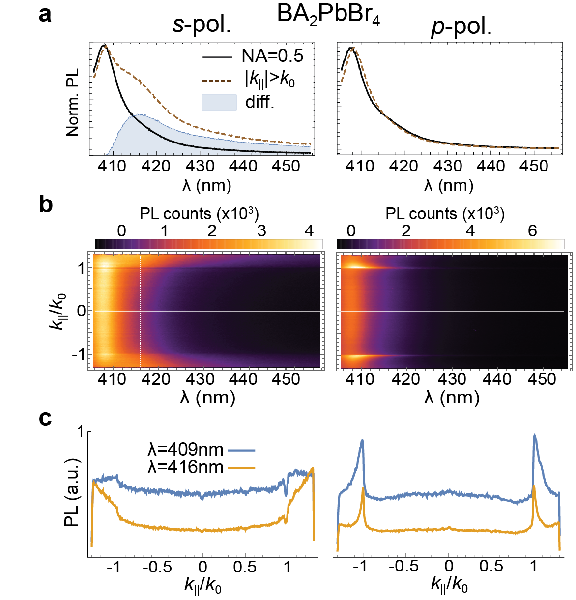 Figure 1
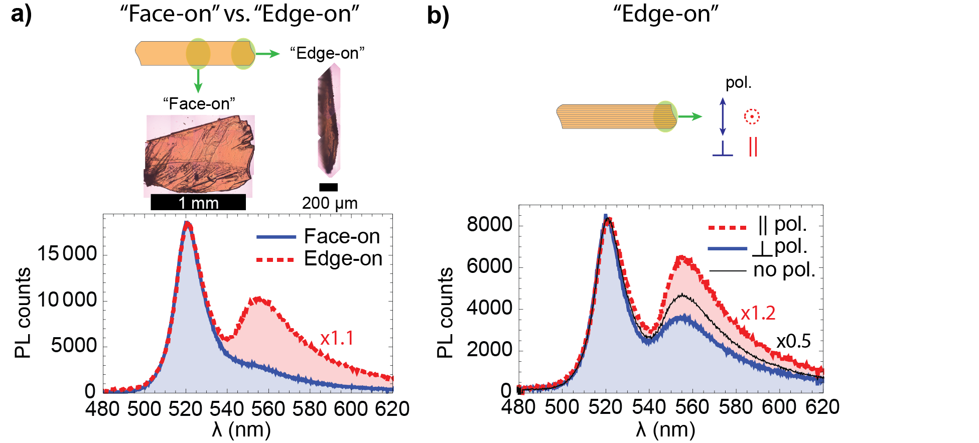 Figure 2
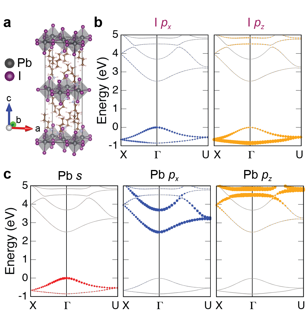 Figure 3
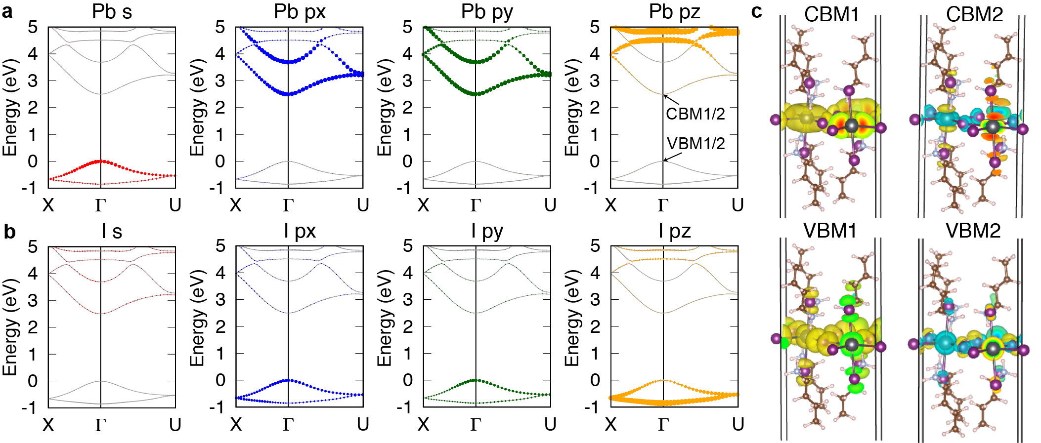 Figure 4
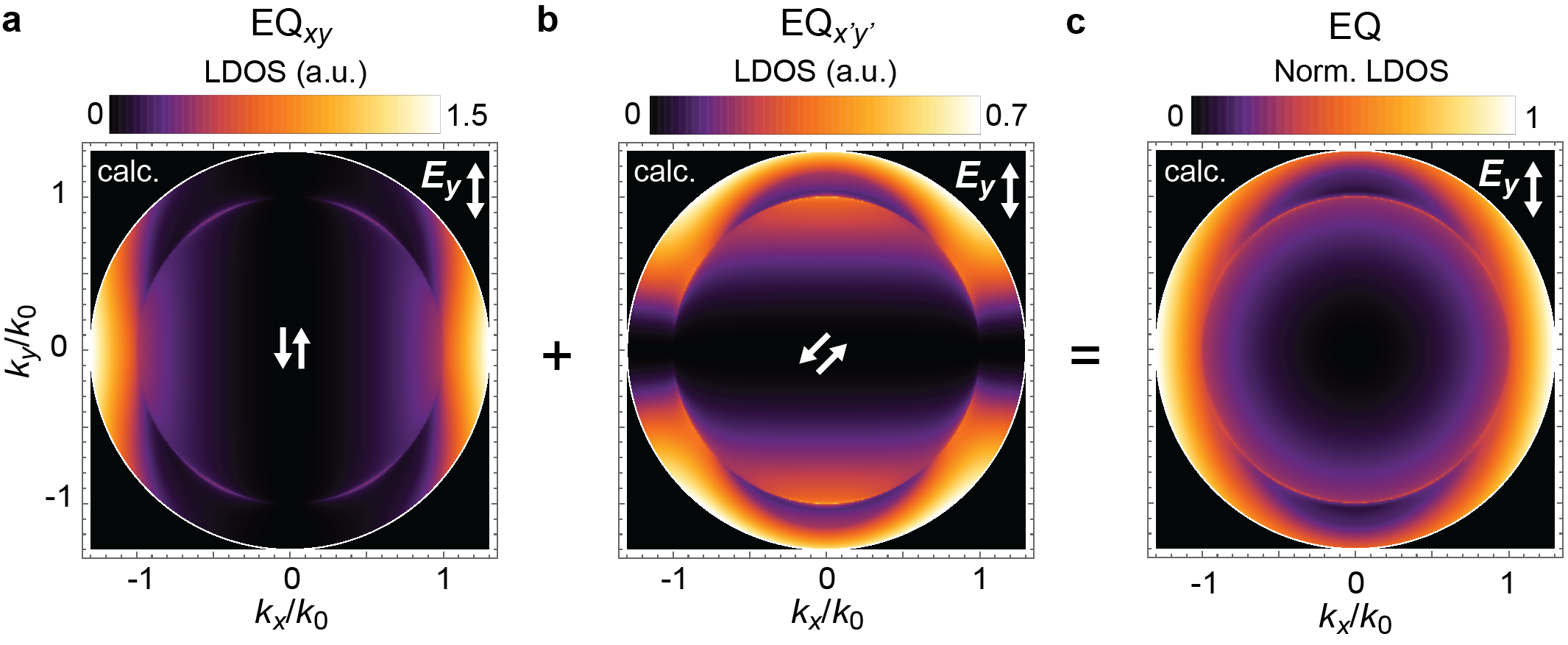 Figure 5
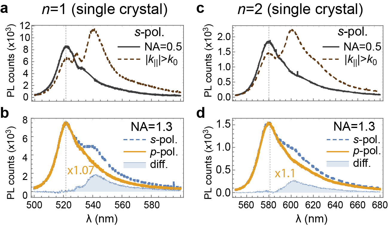 Figure 6
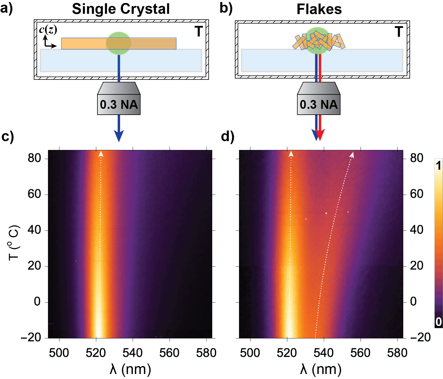 Figure 7
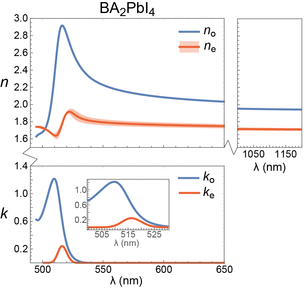 Figure 8
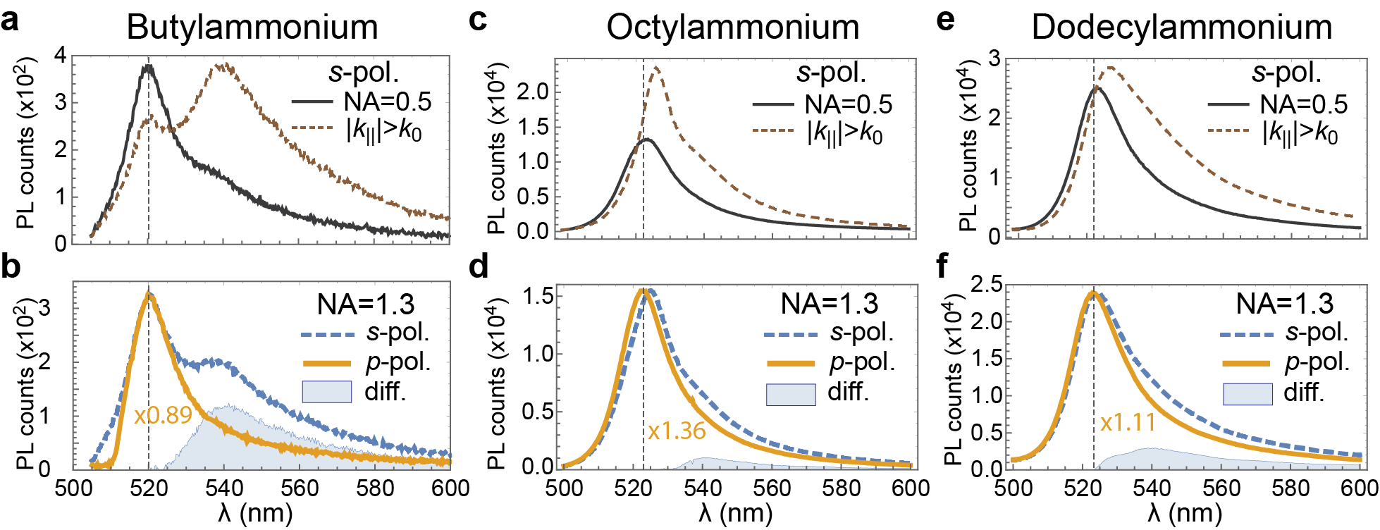 Figure 9
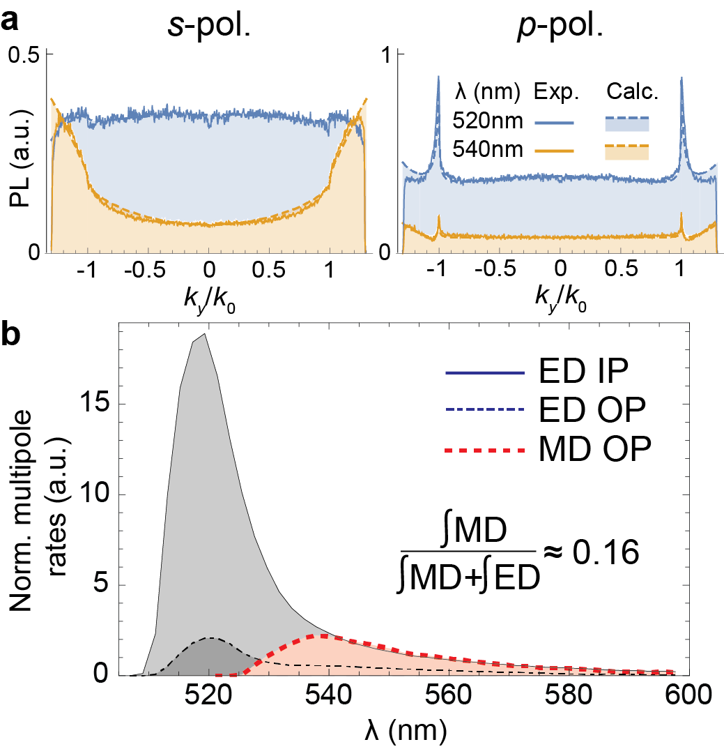 Figure 10
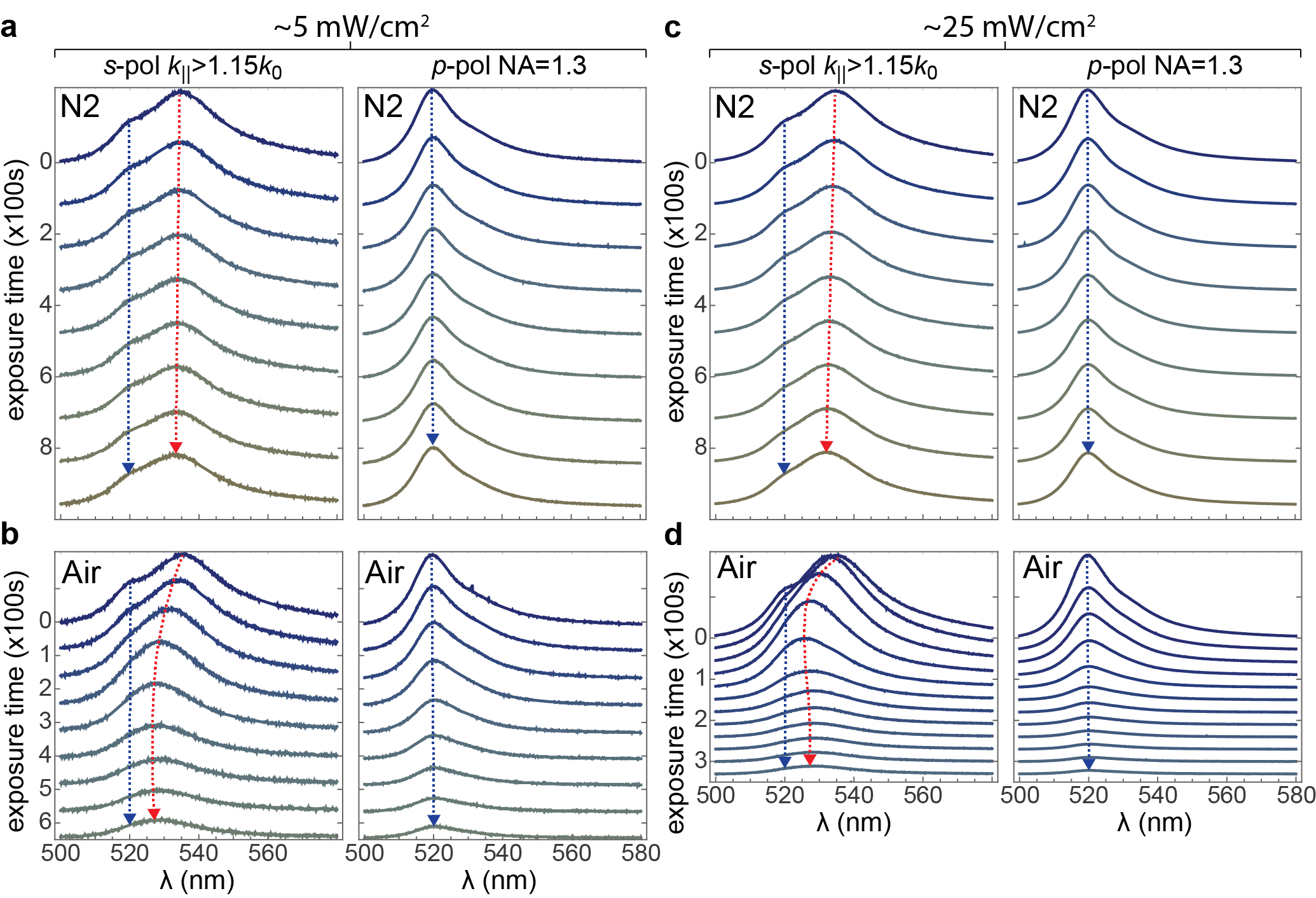 Figure 11
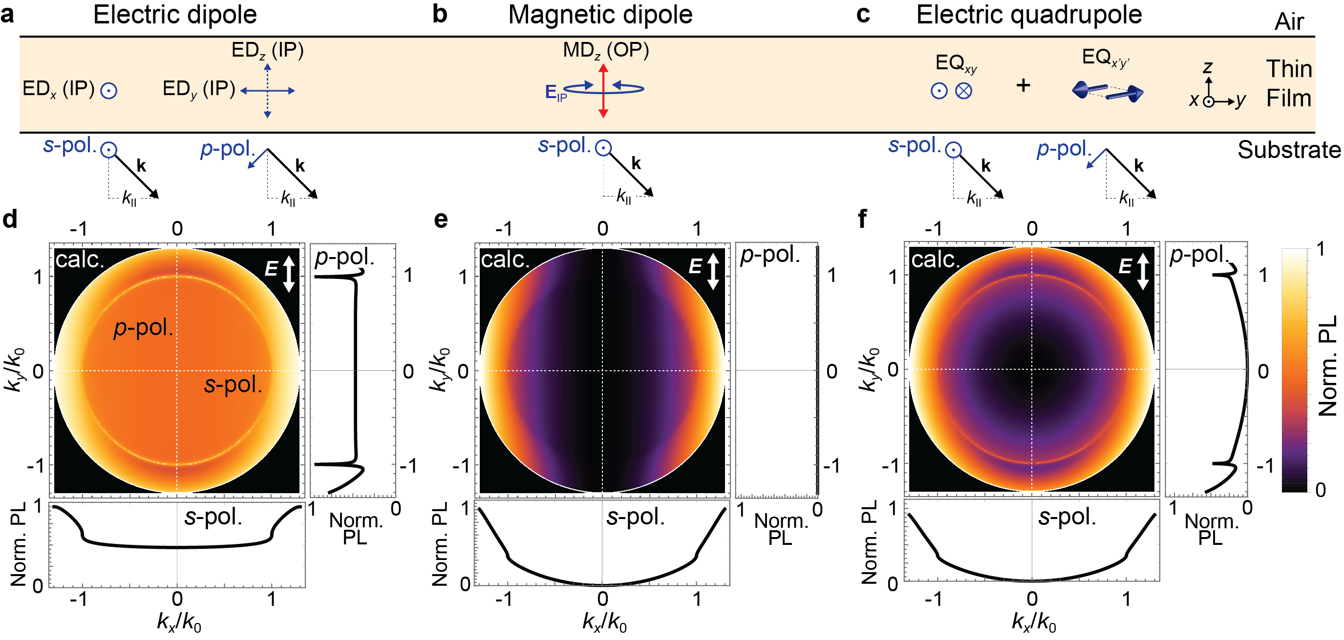 Figure 12
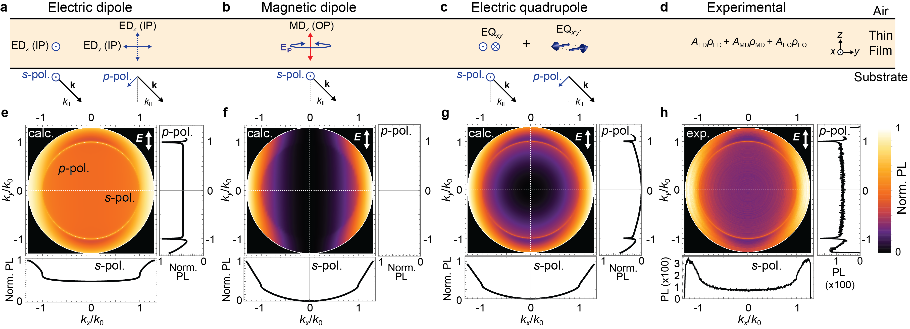 Figure 13
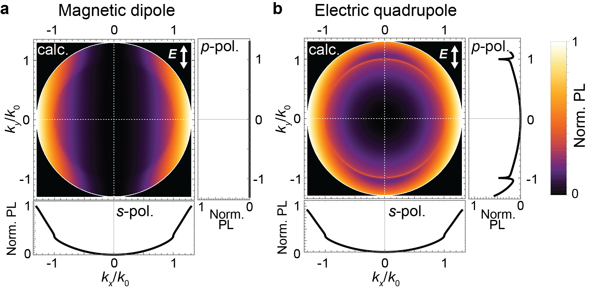 Figure 14
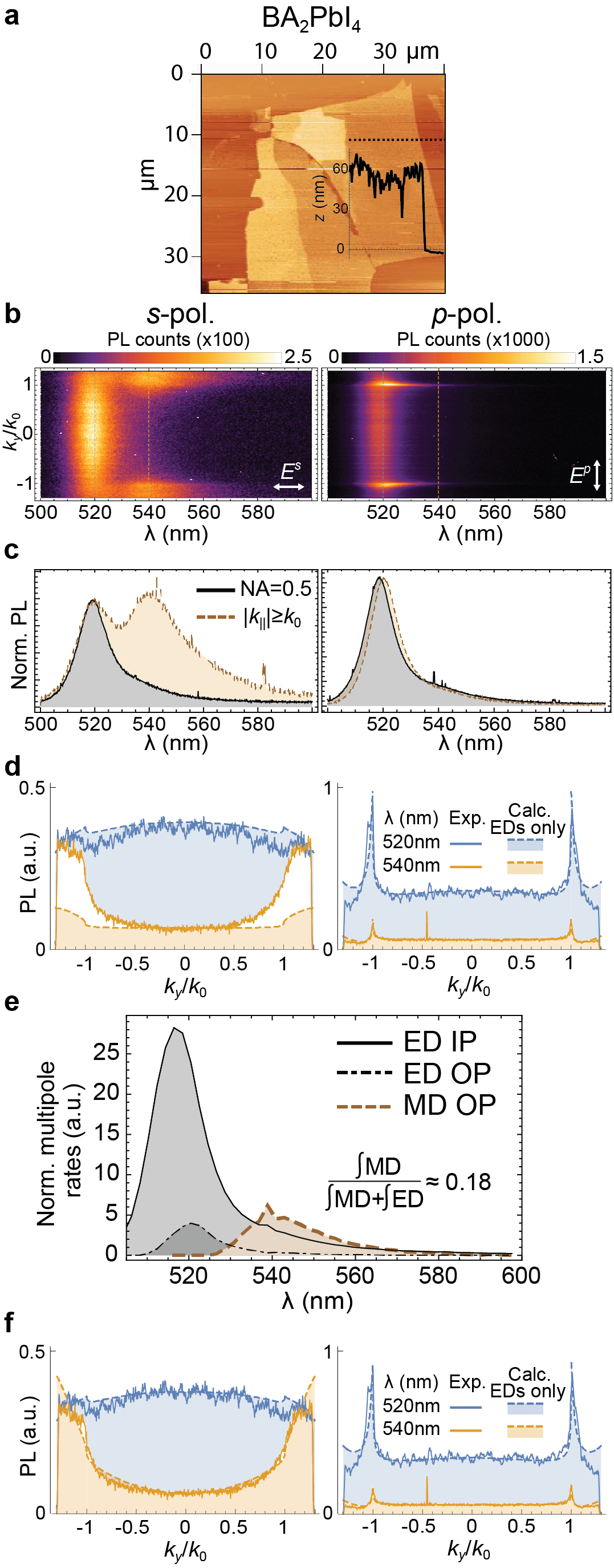 Figure 15
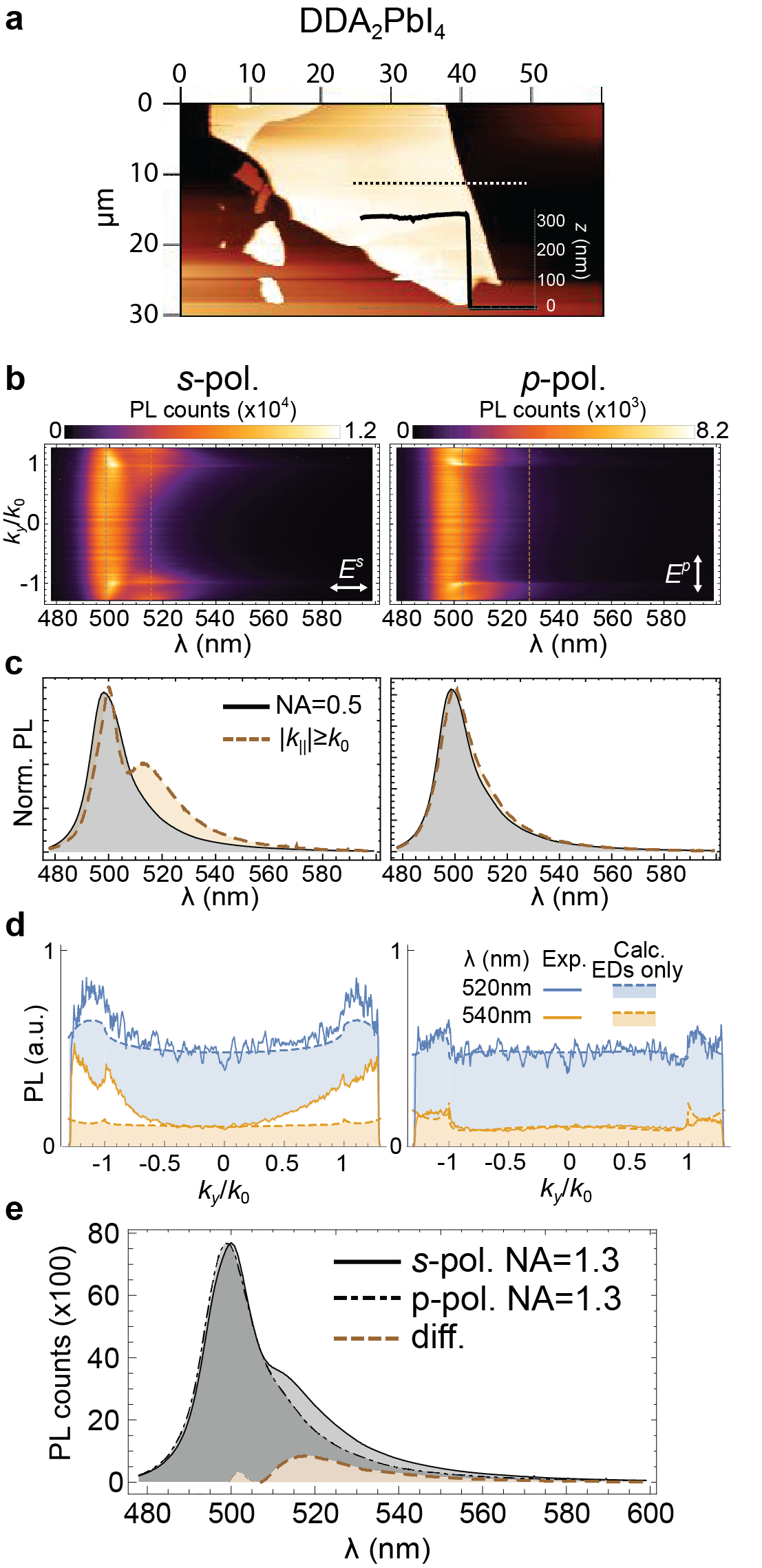 Figure 16
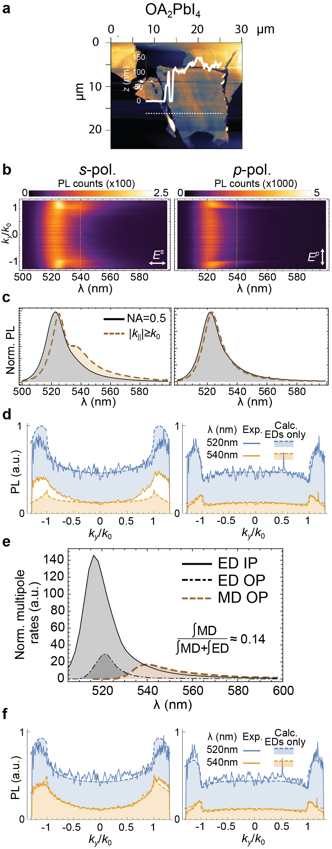 Figure 17
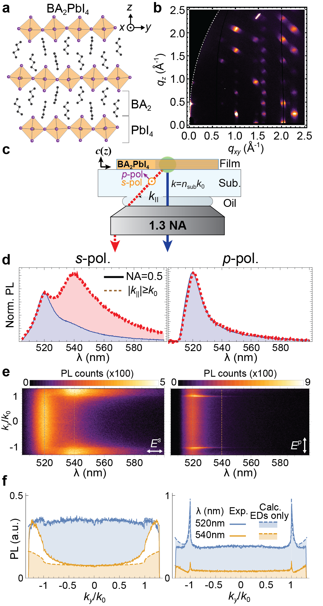 Figure 18
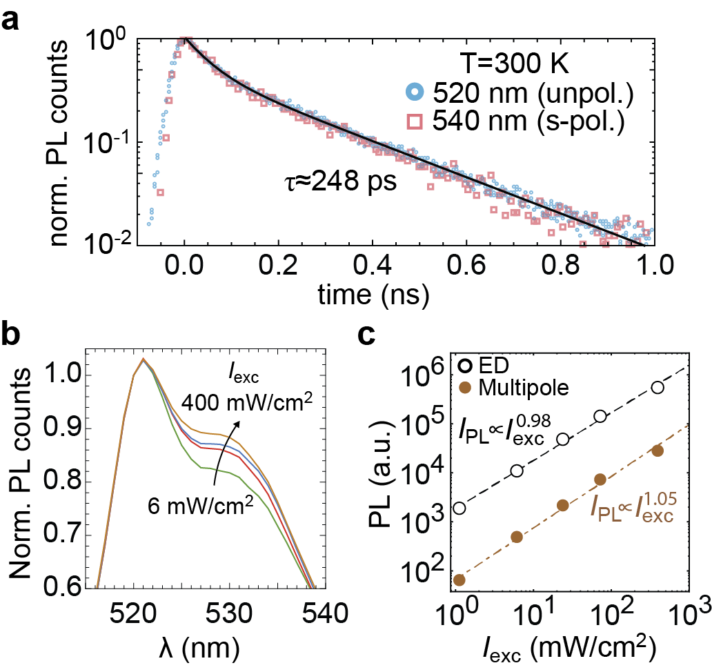 Figure 19
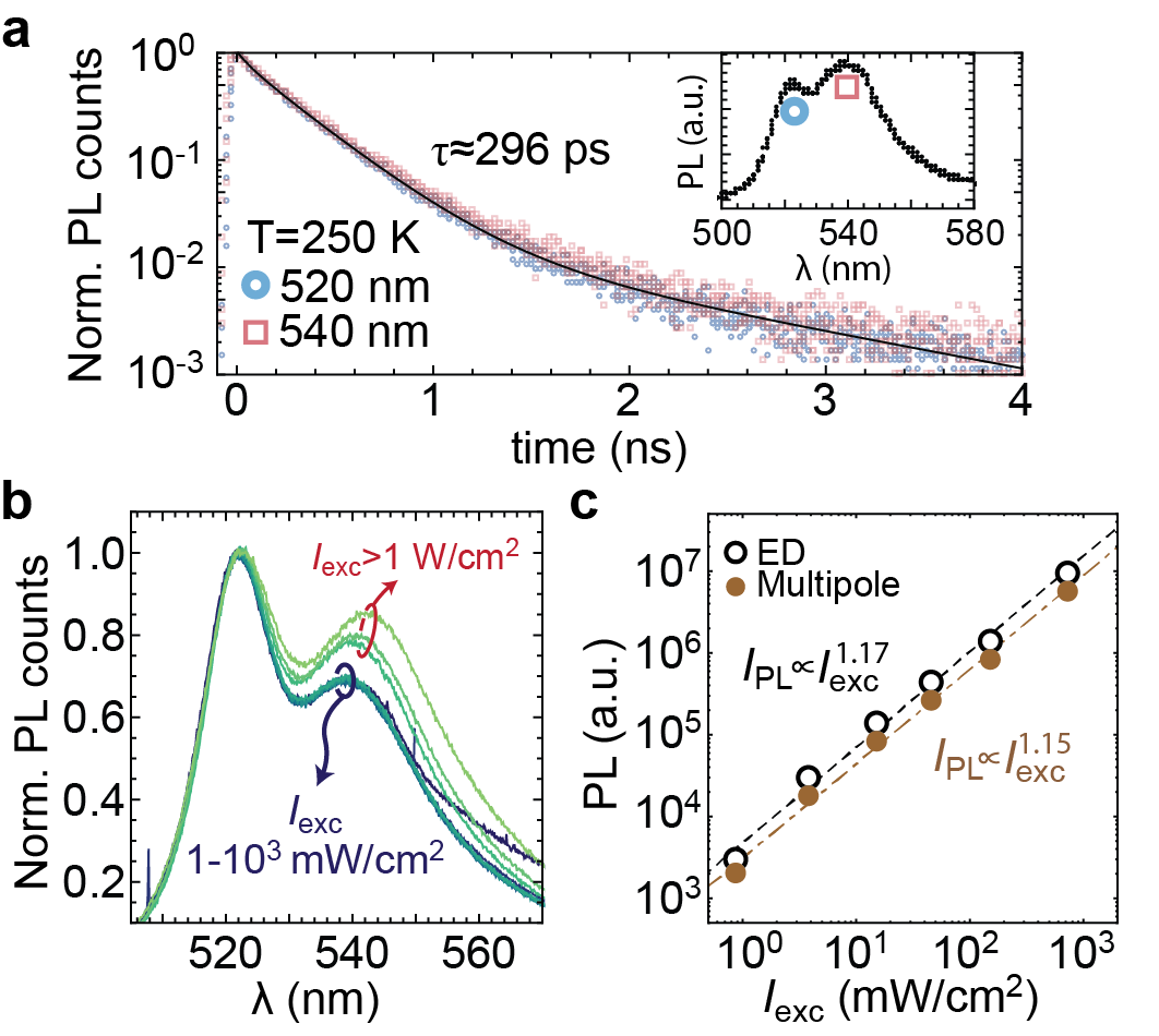 Figure 20
Peer Reviews
No public reviews on file for this paper yet. If you reviewed it on a platform where reviews are public (OpenReview, ICLR, NeurIPS, ICML), you can paste yours below so the community can read it here.
Videos
No videos yet. Explain this paper in a talk, walkthrough, or lecture? Add one.
**Bright magnetic dipole radiation from two-dimensional lead-halide perovskites
**
Ryan A. DeCrescent,1 Naveen R. Venkatesan,2 Clayton J. Dahlman,2 Rhys M. Kennard,2 Xie Zhang,2 Wenhao Li,3, Xinhong Du,4 Michael L. Chabinyc,2 Rashid Zia3 and Jon A. Schuller*,4
1Department of Physics, University of California Santa Barbara, Santa Barbara, CA 93106, USA
2Materials Department, University of California Santa Barbara, Santa Barbara, CA 93106, USA
3Brown University, School of Engineering, Providence, Rhode Island 02912, USA.
4Department of Electrical and Computer Engineering, University of California, Santa Barbara, California 93106, United States
*Correspondence should be addressed to J.A.S. (email: [email protected])
ABSTRACT
Light-matter interactions in semiconductor systems are uniformly treated within the electric dipole (ED) approximation, as multipolar interactions are considered “forbidden”. Here, we demonstrate that this approximation inadequately describes light emission in novel two-dimensional hybrid organic-inorganic perovskite materials (2D HOIPs) — a class of solution processable layered semiconductor with promising optoelectronic properties. Consequently, photoluminescence (PL) spectra become strongly dependent on the experimental geometry, a fact that is often overlooked, though critical for correct optical characterization of materials. Using energy-momentum and time-resolved spectroscopies, we experimentally demonstrate that low-energy sideband emission in 2D HOIPs exhibits a highly unusual, multipolar polarization and angle dependence. Using combined electromagnetic and quantum-mechanical analyses, we attribute this radiation pattern to an out-of-plane oriented magnetic dipole transition arising from the 2D character of the excited and ground state orbitals. Symmetry arguments point toward the presence of significant inversion symmetry-breaking mechanisms that are currently under great debate. These results provide a new perspective on the origins of unexpected sideband emission in HOIPs, clarify discrepancies in previous literature, and generally challenge the paradigm of ED-dominated light-matter interactions in novel optoelectronic materials.
BODY
Hybrid organic-inorganic perovskites (HOIPs) are a rapidly burgeoning class of semiconductors, offering benefits of solution processability, outstanding optoelectronic properties, and the ability to form both three-dimensional (3D) and quantum confined structures.1, 2, 3, 4 Of particular interest for photonic applications, 2D HOIPs incorporating large alkylammonium molecules (e.g., butylammonium lead iodide, BA2PbI4; Fig. 1a) offer additional structural and quantum degrees of freedom, providing continuously tunable band-gap energies and desirable narrow excitonic luminescence.5, 6, 7, 8, 9, 10 Indeed, researchers have demonstrated stable light-emitting diodes9, 11, 12 (LEDs) with high quantum efficiencies,11, 13 as well as low-threshold optical gain.14 However, numerous studies reveal anomalous and undesirable absorption and emission sideband features in both 2D15, 16, 17, 18, 19, 20, 11, 21, 22 and 3D HOIPs,23, 24, 25, 26 leading to “intrinsic white-light emission” that is detrimental to color purity.
Insofar as 2D HOIPs are comprised of alternating semiconducting (metal halide) and insulating (organic) layers, they are recognized as “natural” quantum-well semiconductor structures.27, 28, 29, 30, 31, 32, 5, 8, 33, 34 Accordingly, light-matter interactions in HOIPs are treated by analogy to widely studied conventional semiconductors, such as GaAs.27, 35, 36, 37, 38, 39, 40, 41 Namely, optical transitions are assumed to be completely described by the lowest-order term in a multipolar expansion of the Hamiltonian — the electric dipole (ED) interaction — as higher-order interactions are conventionally slow enough to be considered “forbidden”.42, 43, 44 Operating within this conventional framework, researchers have attempted to identify the origin of anomalous low-energy sideband features in 2D and 3D HOIPs, arriving at interpretations ranging from bound- or bi-exciton emission45, 46, 47, 48 to strong phonon-carrier interactions,49, 16, 17, 19, 50, 21, 19 and in other cases remaining utterly unexplained.15 Recent evidence of more “exotic” and fundamentally interesting physics, such as strong Rashba and Dresselhaus couplings51, 52 and an unconventional exciton fine structure,40, 41, 53 reflect the interplay of strong spin-orbit coupling, structural complexity,54, 55 and the possibility of significant dynamic symmetry-breaking mechanisms.56, 57, 58, 26 Regardless of the mechanism, the observed strength of this sideband emission varies dramatically and curiously between these reports, tempting a judgement of sample quality.
Here, using energy-momentum spectroscopy, we demonstrate that the low-energy sideband emission in 2D HOIPs exhibits a peculiar polarization and angle dependence which is intrinsically related to the 2D nature of the material. Energy-momentum spectroscopies have surfaced as powerful techniques for identifying anisotropic and multipolar optical phenomena in thin film systems.59, 60, 61, 62, 63, 64, 65, 66, 67 For example, by analyzing momentum- and polarization-dependent luminescence profiles, researchers have quantified distinct magnetic dipole (MD) and ED optical transitions in lanthanide59, 62 and transition-metal ions,61 and have identified distinct interlayer excitons in organic semiconductor thin films.60 Using combined electromagnetic and quantum-mechanical analyses, we attribute the anomalous PL from 2D HOIPs to an out-of-plane MD transition from an excitonic state. Symmetry considerations point toward the existence of electronic symmetries that are not revealed in static DFT calculations, supporting the presence of significant dynamical symmetry breaking mechanisms that have recently been suggested.56, 57, 58, 26 This demonstrates the critical role of the experimental geometry in the optical characterization of novel 2D materials, and likely accounts for the wide variation of previous interpretations of sideband emission in HOIPs.
While the features described herein seem to be generic to the material system, including 3D HOIPs, we exploit the highly oriented and 2D nature of BA2PbI4 (Fig. 1a) to relate the unusual radiation patterns to the underlying quantum mechanical origins. Figure 1b shows measured grazing incidence wide-angle X-ray scattering (GIWAXS) patterns from a spin-cast thin film of BA2PbI4. This data is consistent with a vertically layered structure in which PbI4 monolayers are separated by BA2 spacer layers in the out-of-plane () direction.68, 69 The wavelength-dependent uniaxial complex refractive index (Supplementary Fig. 1) of these samples was determined by a combination of momentum-resolved reflectometry64 and variable-angle spectroscopic ellipsometry (Methods; Supplementary Information S1). Films exhibit a predominant in-plane (IP) optical response with weak out-of-plane (OP) dispersion, similar to high-quality single crystals45, 70 and consistent with the vertically layered orientation as determined from GIWAXS. By the nature of the spin-casting method, the resulting films are polycrystalline and thus rotationally isotropic over microscopic length scales relevant for the measurements performed here (100 m).68 The highly oriented and rotationally invariant thin-film structure facilitates detailed analysis of momentum- and polarization-dependent optical phenomena using the experimental geometry illustrated in Fig. 1c. However, as we will describe later, the same features are observed from high-quality single crystals and our conclusions are thus not restricted to spin-cast films. In energy-momentum spectroscopy, both the in-plane electromagnetic momentum (=\langle$$k_{x},k_{y}$$\rangle) and wavelength () distribution of polarized reflection or luminescence are simultaneously measured by imaging the Fourier plane (i.e., back focal plane; BFP) of a collection objective onto the entrance slit of an imaging spectrometer. Polarized spectra are acquired by placing a linear polarizer in the collection path oriented either perpendicular () or parallel () to the entrance slit (-axis). Figures 1d-f show - (left) and -polarized (right) energy- and momentum-resolved PL measured from a 61 nm spin-cast film of BA2PbI4 at room temperature (Methods).
As seen in Figure 1d, -polarized PL spectra collected above the total-internal-reflection condition =|k_{y}|$$>$$k_{0} (red dashed) are dramatically different than conventional spectra as collected by a 0.5 NA objective (; blue). Both - (left) and -polarized (right) spectra exhibit the well-established excitonic emission feature at 520 nm. However, a distinct emission feature at 540 nm (90 meV energy difference), apparent as a subtle shoulder at low momenta (blue),
becomes the dominant emission feature at high momenta (red dashed). In contrast, this emission feature is virtually absent at all momenta in -polarized spectra. This difference in momentum distributions is even more striking when we examine the full energy-momentum spectra (Figure 1e; polarization orientation indicated by white arrows). The low-energy emission feature is readily observed as two bright lobes in the -polarized spectra at |k_{||}|$$>$$k_{0}. Importantly, the -polarized emission features at 520 nm and 540 nm have markedly distinct curvature in -space (Fig. 1f; left). The emission feature at 520 nm (blue) is maximal near normal (=0) and exhibits a slow roll-off into higher momenta; the opposite is true for emission at 540 nm (orange). This illustrates the critical role of the experimental geometry on the inferred significance of this emission (Supplementary Fig. 2); because this light is emitted at highly oblique angles with respect to the crystal axis, it would be ordinarily be trapped (i.e., wave-guided) within the high-index substrate, or within the material itself, and thus only weakly collected with conventional PL geometries (e.g., blue lines in Fig. 1d). This is a general concern for 2D materials, since the polarization and directionality of the emitted light is interacting with highly anisotropic electronic wave functions. This may also have significant implications for optoelectronic devices, especially LEDs, based upon 2D HOIPs; the bandwidth of emission can be enhanced by strategically collecting and redirecting this highly oblique light. Alternatively, the narrow excitonic emission can be retained by allowing this oblique low-energy light to remain trapped in wave-guided modes.
Calculated -polarized PL counts (Supplementary Information S2), assuming only the existence of ED emission, are shown in Fig. 1f (dashed lines) at both 520 nm (blue) and 540 nm (orange). Experimental PL at the 520 nm (primary exciton) emission is accurately described by the ED theory, consistent with an ED-allowed excitonic transition involving CBM and VBM states.71, 36 The 540 nm emission feature, however, is poorly modeled by the same theory. In contrast, -polarized PL at both 520 nm and 540 nm are well-described by ED-only theory. While low-energy emission shoulders have been observed in conventional PL spectra of both inorganic and hybrid organic-inorganic perovskites, 45, 15, 46, 17, 19, 47, 50, 11, 21, 20, 22, 48, 26 none of these prior works examined the polarization and momentum dependence reported here. Note that this theory completely accounts for reabsorption effects by including the complex (uniaxial) refractive index (Supplementary Fig. 1) of the material, thus excluding reabsorption as a possible explanation of the secondary peak. The strong high- emission excess observed predominantly in -polarization cannot be explained by any combination of oriented ED transitions in a rotationally invariant system; a distinct ED transition centered around 540 nm would contribute with equivalent weight to both - and -polarized spectra, inconsistent with our data. The results presented here thus unambiguously demonstrate that this emission is multipolar in nature.
We observe similar multipolar features at high momenta in a number of related HOIPs (Methods; Supplementary Infor-
mation S3), including drop-cast single crystals of the “bilayer” system BA2(CH3NH3)Pb2I7 (Supplementary Fig. 3), thin films of BA2PbBr4 (Supplementary Fig. 4), and films prepared with longer alkylammonium cations (octylammonium and dodecylammonium) (Supplementary Fig. 5). We also find that this feature is robust to sample preparation methods, and is particularly apparent in high-quality single crystals prepared with various alkylammonium cations (including phenethylammonium), and flakes mechanically exfoliated from such crystals (Supplementary Figs. 6-8). We thus conclude that this feature is general to the material system, and is robust against sample preparation methods and substitutions of both the halide and spacer molecules.
While this feature is regularly observed at 540 nm in exfoliated single crystals, we note that, for similarly prepared BA2PbI4 thin films, this emission feature is observed with varying strength at a range of energies between 45-90 meV below the primary emission peak. Analyses of thin-film PL spectra under varying illumination and environmental conditions (Supplementary Information S4; Supplementary Fig. 9) suggest that this variation is due, in part, to the incorporation of oxygen or water72, 73 under various processing conditions. Note, however, that prolonged illumination in ambient conditions significantly reduces the resolution of two distinct peaks, which possibly explains why this feature is so apparent in single crystals. Importantly, this indicates that this sideband does not originate from atmospheric effects (e.g., water or oxygen), but rather seems to be hindered by them.
The highly -polarized nature of the excess (i.e., non-ED) PL provides strong clues for the origins of the multipolar radiation. The candidate oriented multipoles that emit highly oblique -polarized light are OP MDs and IP EQs (Supplementary Information S5; Supplementary Fig. 10). Calculated 2D -polarized radiation patterns from these multipoles are presented in Fig. 2 with - and -polarized -space linecuts shown below and to the right of each 2D image, respectively. OP MDs (“MDz”; Fig. 2a) are associated with a circulating IP electric field and thus produce only -polarized radiation. However, this -polarized MDz contribution is functionally identical to -polarized emission from IP EQs (Fig. 2b; Supplementary Information S2). Although either MD or EQ terms can be used to fit the -polarized emission anomaly, identifying the correct multipole term is important for determining the underlying quantum-mechanical origins. To this end, the OP MD and IP EQ can be distinguished by the fact that the OP MD emits no -polarized PL; in contrast, IP EQs contribute significantly to both - and -polarized spectra (Supplementary Fig. 11). Critically, our data shows virtually zero PL excess in -polarized spectra (Fig. 1d), indicating that the multipolar PL is associated with a highly oriented OP MD transition. Note that, while the ED radiation patterns possess features similar to those of the EQ, the preceding discussion is focused solely upon the patterns associated with the excess counts (i.e., those not already accounted for by the ED theory). We suspect the very subtle shoulder observed in high- -polarized spectra is due to depolarization scattering from surface texture or slightly tilted crystallite domains in spin-cast thin films. Equivalent analyses on mechanically exfoliated single crystals (Supplementary Fig. 6), in which these imperfections are minimized, show no such -polarized shoulder and confirm the MD assignment.
The energy-momentum spectra, in combination with the known material optical constants (Supplementary Fig. 1), afford the opportunity to quantify the relative intrinsic multipolar transition rates. At each wavelength, we decompose the momentum distribution of polarized PL counts, , into a linear combination of oriented EDs and OP MDs (Methods; Supplementary Information S2) according to Eqn. 1:
[TABLE]
Here, the are the normalized local density of optical states (LDOS) into which the oriented dipoles may emit, are the wavelength-dependent intrinsic emission rates, and is a constant factor accounting for setup-specific experimental parameters. Analytical forms for the LDOS are presented in Supplementary Information S2. Including the MD contribution, we now see that the experimental radiation patterns for both polarizations are very well represented by the theory across all wavelengths (Fig. 3a). The resulting decomposed spectra are presented in Fig. 3b. The ED and MD peaks resolved in Fig. 3c are observed as genuinely distinct transitions. The ED (black) and MD (dashed red) contributions exhibit similar asymmetric lineshapes characteristic of luminescence from quantum wells, suggesting that the MD transition also originates from an excitonic excited state. However, the MD emission is notably more broad with an exponential-like distribution of states below the band-gap, characteristic of the Urbach tails that are common in ionic crystals and induced by thermal disorder.74, 26
Although multipolar emission is usually orders of magnitude weaker than ED emission, the multipolar contribution
in BA2PbI4 exhibits an integrated magnitude [] comparable to that of the ED, i.e.,
[TABLE]
As described below, such a strong multipolar PL contribution is highly unusual and particularly unexpected when we consider the overall fast dynamics of the system. In lanthanide ions, for instance, multipolar PL is observed due to long-lived (100 s) excited states associated with ED-forbidden recombination channels.75, 76 Here, however, we observe sub-ns PL lifetimes for the main excitonic feature at 520 nm (Fig. 4a, blue circles). PL decay traces were measured at reduced temperature (250 K), at which phonon-induced population exchange between these two states is reduced26 (Methods). Still, PL traces of the isolated 540 nm feature (Methods) (Fig. 4a, red squares) show no discernible differences; both traces are well represented by a bi-exponential decay with a primary component lifetime of \tau$$\approx296 ps, consistent with previous reports. 19, 77, 78, 79, 80, 41 Unfortunately, this particular material shows a structural phase transition81 below approximately 250 K, at which point the PL spectrum changes abruptly. While two distinct PL peaks separated by 90 meV are indeed visible in this low-temperature phase, their identity is ambiguous since
immersion oils cannot be used to perform energy-momentum spectroscopy at these low temperatures. We thus did not explore the detailed behavior of these features as a function of temperature. These two emission features also show nearly identical behavior under intensity-dependent PL. Throughout a very broad range of excitation intensities (=1-750 mW/cm2) the spectral shape is observed to be nearly invariant (Fig. 4b; darker colored lines). Only at extremely high excitation intensities (I_{\text{exc}}$$>103 mW/cm2; lighter colored lines) does the spectrum begin to vary, with the low-energy feature growing in relative strength over the high-energy feature. Moreover, power-law fits of the decomposed spectra (I_{\text{PL}}$$\propto$$I_{\text{exc}}^{\alpha}) (Fig. 4c) reveal that both the ED contribution (black; =1.170.05) and the multipolar contribution (brown; =1.150.04) grow super-linearly (\alpha$$>1), but in parallel. Note that the data presented in Fig. 4 was measured from poly-crystalline samples with random crystallite orientations in order to enhance the visibility of the 540 nm emission feature with conventional spectroscopy techniques (Methods), but similar conclusions are made from analogous measurements on spin-cast thin films (Supplementary Information S6; Supplementary Fig. 12). Together, these results suggest that both the ED and MD transitions are intrinsic in origin and are associated with excitonic states in thermal equilibrium, contrary to alternative speculations attributing the low-energy feature to bi-excitons (=2) or bound excitons (\alpha$$<1).
The absolute radiative lifetimes can be estimated from the measured PL lifetime, quantum yield (PLQY), and normalized multipolar emission rates. Assuming that the measured PLQY of 0.4% (Methods) is representative of both emission features, our data implies radiative rates of 1.4107 s*-1* and 1.9106 s*-1* for the ED and MD respectively, assuming the emission arises from identical exciton densities. (Note that this PLQY is comparable to previously reported values for this material.15, 34, 9) However, considering the 90 meV energy splitting, the observed low-energy (MD) transition rate could be enhanced relative to the high-energy (ED) transition due to the thermal occupation of excited states. If we assume two distinct emissive channels in thermal equilibrium,82 the intrinsic MD radiative rate is reduced by a factor of exp(90 meV/26 meV)30, yielding an intrinsic radiative rate of 6.0104 s*-1*. Even with this more conservative estimate, the inferred multipolar radiative rate is three orders of magnitude larger than any MD emission rate reported from atomic systems.76 There is, to our knowledge, no crystalline system to which this may be compared. The multipolar emission observed in BA2PbI4 is extraordinarily bright and challenges conventional understanding of multipolar light-matter interactions.
We now consider the electronic band structure as it relates to the origins of the multipolar PL signature. Density functional theory (DFT) calculations (Methods) of the BA2PbI4 electronic structure are summarized in Fig. 5. At each wave vector, , along the -X and -U directions of the reciprocal lattice, we project the ground-state eigenfunctions onto a basis consisting of I (Fig. 5b) and Pb (Fig. 5c) orbitals with
symmetries corresponding to , , , and orbitals. The weight of the projection is represented by the size of the circle at each . The VBM (set to 0 eV in the band diagrams) comprises roughly equal contributions from I (5) orbitals and Pb (6) orbitals, in agreement with previous reports.71, 36, 83, 84 (I and Pb contributions are not shown since they are nearly identical to , due to the system’s approximate symmetry.) Note, however, that the I contribution is significantly suppressed relative to the in-plane contributions. The CBM comprises nearly equal contributions of Pb (6) and (6) orbitals with an absent contribution, in agreement with ref. 36. (See Supplementary Fig. 13 for the complete set of band character projections and charge density plots.) The symmetries of the CBM and VBM states participating in optical transitions, however, are governed by the bonding character of the constituent atoms. Previous studies have assigned (“-like”) and (“-like”) symmetries to the CBM and VBM wavefunctions, and , respectively.35, 36 In analogy with conventional semiconductors, these states may be qualitatively represented by and (CBM), and (VBM); the presence of a predominantly IP ED transition is described by a symmetry analysis of the ED matrix elements between CBM and VBM states: \langle S|x|X\rangle$$\approx$$\langle S|y|Y\rangle and \langle S|z|\psi_{\text{CBM}}\rangle$$\approx0.36 The non-zero EDz contribution observed here and in previous experiments67, 70 may arise from a non-negligible I contribution at the VBM and an I (5) contribution at the CBM (Supplementary Fig. 13). (While electron-hole correlations yield three distinct exciton levels with symmetries corresponding to the direct product of \Gamma_{6}^{-}$$\otimes$$\Gamma_{6}^{+}, the selection rules still reflect the underlying VBM and CBM states and these conclusions are thus unaltered.) This treatment has been used with apparent success to describe the low-temperature exciton spectrum observed in previous reports.27, 35, 36, 38, 37, 85, 39, 40, 41
In contrast to the ED term, the second-order terms of the multipolar expansion (i.e., MD and EQ) connect states with equal parity;44 these multipolar transitions are strictly forbidden within the aforementioned treatment. Our experimental results thus suggest the presence of structural asymmetries that generate CBM and/or VBM states of mixed parity.75 Nonetheless, static DFT calculations reveal negligible static structural asymmetries, evidenced by both the spatial structure of the electronic wave functions36 (Supplementary Fig. 13) and the absence of Rashba-like splitting of the energy bands (Fig. 5).5, 55, 54, 57 A surge of recent reports highlight the importance of dynamic symmetry-breaking mechanisms, e.g., significant thermally-induced polar lattice distortions of the relatively “soft” ionic lattice. 74, 52, 86, 56, 58, 87, 88, 26 For example, “dual emission” characteristics observed in HOIPs have been attributed to a distribution of indirect tail states caused by Rashba-like band splitting originating from large local polar distortions.26 Our observations are generally consistent with this report, but suggest a very different physical mechanism; rather than ED-mediated indirect transitions from Rashba split bands,52, 54, 55, 58, 87, 88, 26 relaxation may instead proceed from significantly perturbed states by direct transitions via the MD term. Such a dynamical origin likely also accounts for the relatively long Urbach-like tail observed for the MD transition.74, 26 Symmetry-based analysis of multipolar matrix elements is detailed in Supplementary Information S8. Qualitatively, MDz connects states with equivalent parity associated with in-plane extended orbitals. Since symmetry (associated with in-plane -like orbitals) has already been assigned to the CBM, a possible explanation is the presence of a yet-to-be established odd-parity contribution to the VBM with strong in-plane character, deriving primarily from the contribution of I (5) orbitals (e.g., see Fig. 5b). These underlying selection rules hold when the excitonic character of the excited state is considered,35, 41 and different electron-hole exchange energies arising from the presence of an additional term in the VBM (in combination with exchange and crystal field effects) may account for a portion of the observed 90 meV energy splitting.
Note that this symmetry-based treatment does not provide estimates of the absolute magnitudes of the transitions, and the observed unconventionally fast MD transition impels deeper theoretical examination of atomic and electronic structure in 2D HOIPs. However, a brief examination of the predicted transition rates based on Fermi’s Golden Rule suggests that such a fast MD transition is, in fact, not unreasonable in this material system. For simplicity, we describe ED and MD emitters in a homogeneous, isotropic, non-magnetic environment with refractive index . Fermi’s Golden Rule gives for the spontaneous emission rates from state to state through an MD () channel:89, 59
[TABLE]
where =, is the speed of light, () is the vacuum permittivity (permeability), is Planck’s constant, is the charge of the state in question, and and are the orbital and spin angular momentum operators. While ED rates in crystals are on the order of 107 s*-1*, as observed here, MD and higher-order rates are often considered negligible by dimensional analysis arguments which typically invoke quantities relevant to isolated atoms (r$$\sim$$a_{0}, where is the Bohr radius) in homogeneous free-space (=1), and thus assume bare electron masses (=). Detailed calculations for lanthanide ions76 give vacuum MD rates of 10-30 s*-1*. Taking into account the refractive index (n$$\approx2.3) and the fact that the elementary excitations are states with effective mass m^{*}$$\approx0.1 (rather than the bare electron mass, ), we estimate MD emission rates to be of order /(m^{*}/m_{0})^{2}$$\approx103 times greater than those in free space. This indeed brings us curiously close to the MD emission rate (104 s*-1*) observed here from HOIPs. Since these arguments are general, multipolar phenomena may be more prevalent than previously thought, perhaps existing in other 2D semiconductor systems or ionic crystals with strong spin-orbit coupling, unconventional band structures, heavy atoms (e.g., WSe2.90) and significant lattice dynamics. That they have not readily been established may be a consequence of the rare usage of momentum- and polarization-resolved spectroscopies.
CONCLUSIONS
Using energy-momentum spectroscopies, we establish that the low-energy sideband emission feature frequently observed in HOIPs exhibits an anomalous polarization and angle dependence. These unconventional radiation properties of the sideband luminescence have not yet been acknowledged. Consequently, the magnitude of these transitions has been largely underestimated, and interpretations of the underlying nature and significance of the emission have varied widely. Generally, this demonstrates the critical role of the experimental geometry on optical studies, particularly in the study of highly anisotropic material systems. Indeed, since such anisotropies are inherent to all novel 2D quantum materials, polarization and angle dependencies should be very carefully considered in future studies using conventional optical characterization techniques. These observations are critical for resolving discrepancies in the literature and may be exploited to optimize the functionality of optoelectronic devices, especially LEDs, based upon 2D HOIPs. For instance, the spectrum and dynamics of light emission may be manipulated by controlling this highly oblique multipolar emission with various photonic architectures.91, 62
Exploiting the highly-oriented structure of 2D HOIPs, and taking into account these polarization-, wavelength-, and angle-dependent collection effects, we identify the sideband luminescence as arising from an oriented and exceptionally fast magnetic dipole optical transition. Although multipolar light-matter interactions have been demonstrated in III-V quantum dots, these higher-order interactions derive from mesoscale structuring92 and strong electric field gradients in the vicinity of plasmonic structures.93 That is, the multipolar interactions are characteristic of electronic envelope functions enforced by the structure of the quantum dot rather than the symmetries of the Bloch functions associated with the bulk material. In contrast, the presence of a multipolar transition in 2D HOIPs is evidently inherent to the material system and is understood on the basis of symmetries of the Bloch functions used to describe both the valence and conduction bands. Accounting for these extrinsic collection effects, we show that the MD radiative rate is at least three orders of magnitude larger than multipolar emission rates previously identified in atomic systems;59, 76, 61 there is yet no other crystalline system to which these rates may be compared. This discovery of bright MD luminescence, coupled with first-principles considerations of radiation rates, suggest that multipolar phenomena may be more prevalent than previously thought, particularly in materials with, e.g., strong confinement, large spin-orbit coupling, mixed parity states, or dynamic structural distortions.
Methods
Samples. Solutions of (C4H9NH3)2PbI4 were prepared according to the procedures described in ref. 68 to concentrations of 150 mg/mL in an N2-filled glovebox. Thin films were dynamically spin-cast (solution deposited while spinning) in an N2-filled glovebox on 0.180 mm fused silica substrates at 8000 RPM for 60 seconds and subsequently thermally annealed at 70∘C for 30 minutes, producing films with thicknesses of 61 nm. Film thicknesses were measured with atomic force microscopy (AFM) (Asylum MFP-3D) in tapping mode using a tip-scratch method and measuring over the resulting groove. For variable angle spectroscopic ellipsometry studies, thin films were prepared identically, upon Si substrates. All samples were kept in a nitrogen-vacated dry box immediately following film preparation until the time of optical measurements. Mechanically exfoliated flakes (Supplementary Figs. 5-7) were produced by the “scotch tape method” from single crystals grown according to the methods described in ref. 94 in an N-filled glovebox. Flake thicknesses were determined by AFM in tapping mode after optical measurements were made. Single crystals of (C4H9NH3)2(CH3NH3)n-1PbnI3n+1 with n=1 and n=2 (Supplementary Fig. 3) were grown from solution directly on plasma-cleaned fused silica substrates by drop depositing 7 L of solution (prepared as described above) and allowing the solvent to evaporate at elevated temperatures (45∘C). Samples were subsequently thermally annealed at 100∘C for 10 minutes. Crystals were identified visually by means of an inverted microscope with magnification varying from 10 to 100, and phase purity was confirmed by analyzing the PL spectra (Supplementary Fig. 5). Thin films of (C4H9NH3)2PbBr4 (butylammonium lead bromide; Supplementary Fig. 6) were prepared from (C4H9NH3)2PbI4 thin films by a vapor exchange method according to procedures specified in Supplementary Information S4. Thin films of (C8H17NH3)2PbI4 (octylammonium lead iodide) and (C12H25NH3)2PbI4 (dodecylammonium lead iodide) (Supplementary Fig. 7) were prepared according to the procedures described above with the substitution of butylammonium for octylammonium and dodecylammonium, respectively. For TRPL and pump power-dependence studies (Fig. 4), samples were prepared by the drop-casting method (described above) without initial plasma cleaning of substrates. This strategically produced thick films with mixed crystallite orientations and significant scattering texture by minimizing wetting of the substrate, thereby enhancing the visibility of the 540 nm emission without the use of high-NA imaging techniques.
GIWAXS. Grazing-incidence wide-angle X-ray scattering (GIWAXS) experiments were conducted at the Advanced Light Source at beamline 7.3.3. The energy of the incident beam was at 10 keV and a Pilatus 2M area detector was used. The X-ray scattering data were taken at incidence angles of 0.3∘ and samples were kept in a helium environment during X-ray exposure to minimize air scattering and sample degradation. The collected images were processed using GIXSGUI,95 and the beam center and the sample-to-detector distance were calibrated using silver behenate (AgBe).
Optical constants. Uniaxial optical constants for thin films of (C4H9NH3)2PbI4 were determined by a combination of momentum-resolved reflectometry64 and variable angle spectroscopic ellipsometry. See Supplementary Information S1 for complete details.
Energy-momentum spectroscopy. Thin film samples were illuminated by a 405 nm light-emitting diode (LED) (ThorLabs M405L3). The incident light was filtered by a 405 nm short-pass filter and reflected by a 415 nm dichroic mirror to remove overlap with the emission wavelengths. The emitted PL was transmitted through the same dichroic as well as a 417 nm long-pass filter. The energy and -momentum, , of the light was then measured by imaging the objective (Nikon CFI Plan Fluor 100 Oil, 1.3 NA) BFP to the entrance slit of an imaging spectrometer (Princeton Instruments IsoPlane SCT320 with Princeton Instruments PIXIS 1024BRX). An analyzing polarizer was applied to the image such that light along the -axis was either -polarized (vertical polarizer alignment) or -polarized (horizontal polarizer alignment). For the data presented in Figs. 1 and 3, measurements were performed in ambient conditions with illumination intensities below 1 mW/cm2. The exposed films showed no visible signs of photo-degradation. The resulting energy-momentum spectra were decomposed into various multipolar contributions using methods described elsewhere59, 60 assuming a uniform distribution of dipole/multipole locations along the -axis. Film thicknesses were taken from AFM (see “Samples”). Film optical constants were determined from the same films using methods described completely in Supplementary Information S1. For photo-degradation studies (Supplementary Fig. 11), measurements were performed in both ambient and inert (N2) conditions, and illumination intensities were swept between 5 mW/cm2 and 100 mW/cm2. No visible signs of photo-degradation were observed for samples exposed in inert conditions. Integration times for all measurements were on the order of 10-1000 s, depending upon illumination intensity. For energy-momentum spectroscopy of exfoliated flakes, after sample preparation (see “Samples”), a heavy flow of nitrogen gas was applied to the sample. The nitrogen flow persisted for the duration of the optical measurements. Single crystals and platelets were identified by eye under a 100 oil-immersion objective. Single crystals were illuminated by focusing a 405 nm fiber-coupled laser to the image plane at the rear port of the microscope. At the level of the sample, the focused spot had a width of 5 m. Total illumination intensities were kept below 0.06 W/cm2. Integration times were on the order of 100-1000 s. The exposed crystals showed no significant signs of optical degradation. All energy-momentum spectroscopy measurements and pump-dependent PL measurements were performed at room temperature.
TRPL. Time-correlated single-photon counting measurements (Fig. 4a) were performed in the UCSB Optical Characterization Facility. Approximately 100 fs excitation pulses with wavelength 400 nm were generated by doubling the fundamental frequency of fs Ti:Sapphire laser (Spectraphysics Tsunami) pulses in a commercial optical harmonic generator (Inrad). The laser repetition rate was reduced to 2 MHz by a home-made acousto-optical pulse picker in order to avoid saturation of the chromophore. The system is equipped with thermoelectrically-cooled single-photon counting avalanche photodiode (Micro Photon Devices) and electronics board (Becker & Hickl SPC-630) and has instrument response time 30 ps. The fluorescence signal was dispersed in Acton Research SPC-500 monochromator after passing through long-pass filter to remove the pump wavelength. In addition to the time-resolved detector, the monochromator is equipped with a CCD camera (Roper Scientific PIXIS-400) allowing for monitoring of the time-averaged fluorescence spectrum. To maximize the 540 nm PL signal, films were produced by the drop-casting method as described in “Samples”. Samples were mounted within an evacuated cryostat maintained at 0.510*-5* mBar to avoid photo-degradation. Samples were pumped at 400 nm with 0.025 J/cm2 per pulse with a 2 MHz repetition rate. PL was collected in a reflection geometry with the pump and collection optics at 90∘ with respect to each other and approximately 45∘ with respect to the sample normal. The data shown in Fig. 4a was acquired at 250 K in order to minimize thermally assisted excitation transfer between the states. Analogous measurements presented in the Supporting Information were performed on spin-cast thin films by collecting the PL at high angles (with respect to the sample interfaces) through a linear polarizer in an s-polarized configuration.
Pump-dependent PL. For pump power-dependence studies as presented in Fig. 4b-c, films were prepared according to the drop-casting method as described in “Samples”. Regions with reoriented crystals or sufficient scattering texture were identified visually. The reorientation and/or scattering texture allowed the 540 nm emission to be detected with a 10 0.3 NA (Nikon CFI Plan Fluor). Samples were illuminated by a loosely focused spot (100 m beam waste) in inert (N2) conditions according to the methods described for single crystals above. Illumination intensities were swept between 1 mW/cm2 and 1 W/cm2. No signs of photo-degradation were observed for pump powers below 750 mW/cm2. Integration times for all measurements were on the order of 0.1-250 s, depending upon illumination intensity. Spectra were decomposed to a sum of two (asymmetric) Gaussian distributions with stretched tails and fixed widths. The centers of the distributions were held at 522 nm and 541 nm. Only the amplitudes of the two components were fit at each illumination intensity.
PLQY. PLQY of spin-cast thin films was measured using a Horiba spectrometer (FluoroMax 4) and integrating sphere (Horiba Quanta-) with 400 nm wavelength excitation. To improve PL counts, samples were spin-cast at 1500 rpm resulting in films of 300 nm thickness. The photon absorption rate was determined by scanning over the excitation line of the attenuated beam (nominal OD=3, measured area fill correction of 803) with the sample in place and comparing to a non-absorbing reference (blank quartz substrate). A 405 nm short-pass filter (Semrock) was in place during excitation and emission measurements, and a 405 nm long-pass filter (Semrock) was in place for emission measurements only. A 1% correction factor was applied to account for long-pass transmission efficiencies. We note that the 540 nm emission was clearly visible in integrating sphere PL measurements, as expected since PL is collected over all angles.
Band structure. First-principles calculations were performed based on DFT as implemented in the Vienna Ab initio Simulation Package (VASP)96. We used projector augmented wave (PAW)97 pseudopotentials with a plane-wave energy cutoff of 500 eV. A -centered k-point grid was used for sampling the first Brillouin zone. The Heyd-Scuseria-Ernzerhof (HSE)98 hybrid functional was employed for the exchange-correlation interactions. A mixing parameter of 0.45 was used for the HSE functional including spin-orbit coupling to give a consistent bandgap with experiment. The atomic positions and lattice constants were fully relaxed; the optimized lattice constants were 8.79, 8.80 and 29.07 Å, respectively.
Acknowledgements
Energy-momentum spectroscopy measurements and analyses were supported by the National Science Foundation (DMR-1454260 and OIA-1538893) and by the Air Force Office of Scientific Research (Grant No. FA9550-16-1-0393). Time- and intensity-resolved optical measurements and analyses, and studies of exfoliated single crystals comprising varying organic spacers were supported as part of Quantum Materials for Energy Efficient Neuromorphic Computing, an Energy Frontier Research Center funded by the U.S. Department of Energy (DOE), Office of Science, Basic Energy Sciences (BES), under Award # DE-SC0019273. Materials synthesis and structural characterization were supported by the U.S. Department of Energy, Office of Science, Basic Energy Sciences, under Award DE-SC-0012541. PLQY measurements were performed at the MRL Shared Experimental Facilities are supported by the MRSEC Program of the NSF under Award No. DMR 1720256; a member of the NSF-funded Materials Research Facilities Network (www.mrfn.org). Portions of the work were performed at the Advanced Light Source, supported by the Director, Office of Science, Office of Basic Energy Sciences, of the U.S. Department of Energy under Contract No. DEAC02-05CH11231. A portion of this work was performed in the UCSB Nanofabrication Facility. The research reported here also made use of the shared facilities of the UCSB MRSEC (National Science Foundation DMR 1720256), a member of the Materials Research Facilities Network (www.mrfn.org). R.M.K. gratefully acknowledges the National Defense Science and Engineering Graduate fellowship for financial support. X.Z. was supported by the U.S. Department of Energy (DOE), Office of Science, Basic Energy Sciences (BES) under Award No. DE-SC0010689. Computational resources were provided by the National Energy Research Scientific Computing Center, a DOE Office of Science User Facility supported by the Office of Science of the U.S. Department of Energy under Contract No. DE-AC02-05CH11231. We thank Chris G. Van de Walle and Michael E. Flatte for helpful discussions.
Author contributions
R.A.D., M.L.C., and J.A.S. conceived of the experiment. R.A.D. and W.L. performed optical measurements. R.A.D. performed electromagnetic calculations and analyzed the optical data with R.Z. and J.A.S. R.A.D., N.R.V., C.J.D., R.M.K. synthesized samples. N.R.V., C.J.D. and R.M.K. performed and analyzed GIWAXS measurements with M.L.C. X.Z. performed numerical band structure calculations. J.A.S. supervised the project. All authors discussed the results and commented on the manuscript.
Additional information
Supplementary Information accompanies this paper.
Data availability: The data that support the findings of this study are available from the corresponding author upon reasonable request.
The reference list from the paper itself. Each links out to its DOI / PubMed record.
- 11 Brenner, T.M., Egger, D.A., Kronik, L., Hodes, G. & Cahen, D. Hybrid organic-inorganic perovskites: low-cost semiconductors with intriguing charge-transport properties. Nature Reviews Materials 1 , 15007 (2016).
- 22 Herz, L.M. Charge-carrier dynamics in organic-inorganic metal halide perovskites. Annual Review of Physical Chemistry 67 , 65–89 (2016).
- 33 Zhang, W., Eperon, G.E. & Snaith, H.J. Metal halide perovskites for energy applications. Nature Energy 1 , 16048 (2016).
- 44 GarcÃÂa de Arquer, F.P., Armin, A., Meredith, P. & Sargent, E.H. Solution-processed semiconductors for next-generation photodetectors. Nature Reviews Materials 2 , 16100 (2017).
- 55 Stoumpos, C.C. et al. Ruddlesden-Popper hybrid lead iodide perovskite 2D homologous semiconductors. Chem. Mater. 28 , 2852–2867 (2016).
- 66 Tsai, H. et al. High-efficiency two-dimensional Ruddlesden-Popper perovskite solar cells. Nature 536 , 312–316 (2016).
- 77 Pedesseau, L. et al. Advances and promises of layered halide hybrid perovskite semiconductors. ACS Nano 10 , 9776–9786 (2016).
- 88 Kamminga, M.E. et al. Confinement Effects in Low-Dimensional Lead Iodide Perovskite Hybrids. Chem. Mater. 28 , 4554–4562 (2016).