Zeeman-type spin splitting in non-magnetic three-dimensional compounds: Materials prediction and electrical control
Carlos Mera Acosta, Adalberto Fazzio, Gustavo M. Dalpian

TL;DR
This paper predicts and demonstrates the existence of Zeeman-type spin splitting in non-magnetic three-dimensional compounds, showing it can be controlled electrically and used for spin-filtering devices, expanding beyond two-dimensional materials.
Contribution
It identifies conditions for Zeeman-type spin splitting in 3D compounds, systematically searches for candidates, and shows electric control of spin-splitting and metal-insulator transitions.
Findings
20 candidate materials with Zeeman-type effect identified
Spin-splitting controlled by external electric field
Electric field induces metal-insulator transition
Abstract
Despite its potential for device application, the non-magnetic Zeeman effect has only been predicted and observed in two-dimensional compounds. We demonstrate that non-centrosymmetric three-dimensional compounds can also exhibit a Zeeman-type spin splitting, allowing the splitting control by changing the growth direction of slabs formed by these compounds. We determine the required conditions for this effect: ) non-centrosymmetric including polar and non-polar point groups, ) valence band maximum or conduction band minimum in a generic -point, i.e., non-time-reversal-invariant momentum, and ) zero magnetic moment. Using these conditions as filters, we perform a material screening to systematically search for these systems in the aflow-ICSD database. We find 20 material candidates featuring the Zeeman-type effect. We also found that the spin-splitting in confined systems…
Click any figure to enlarge with its caption.
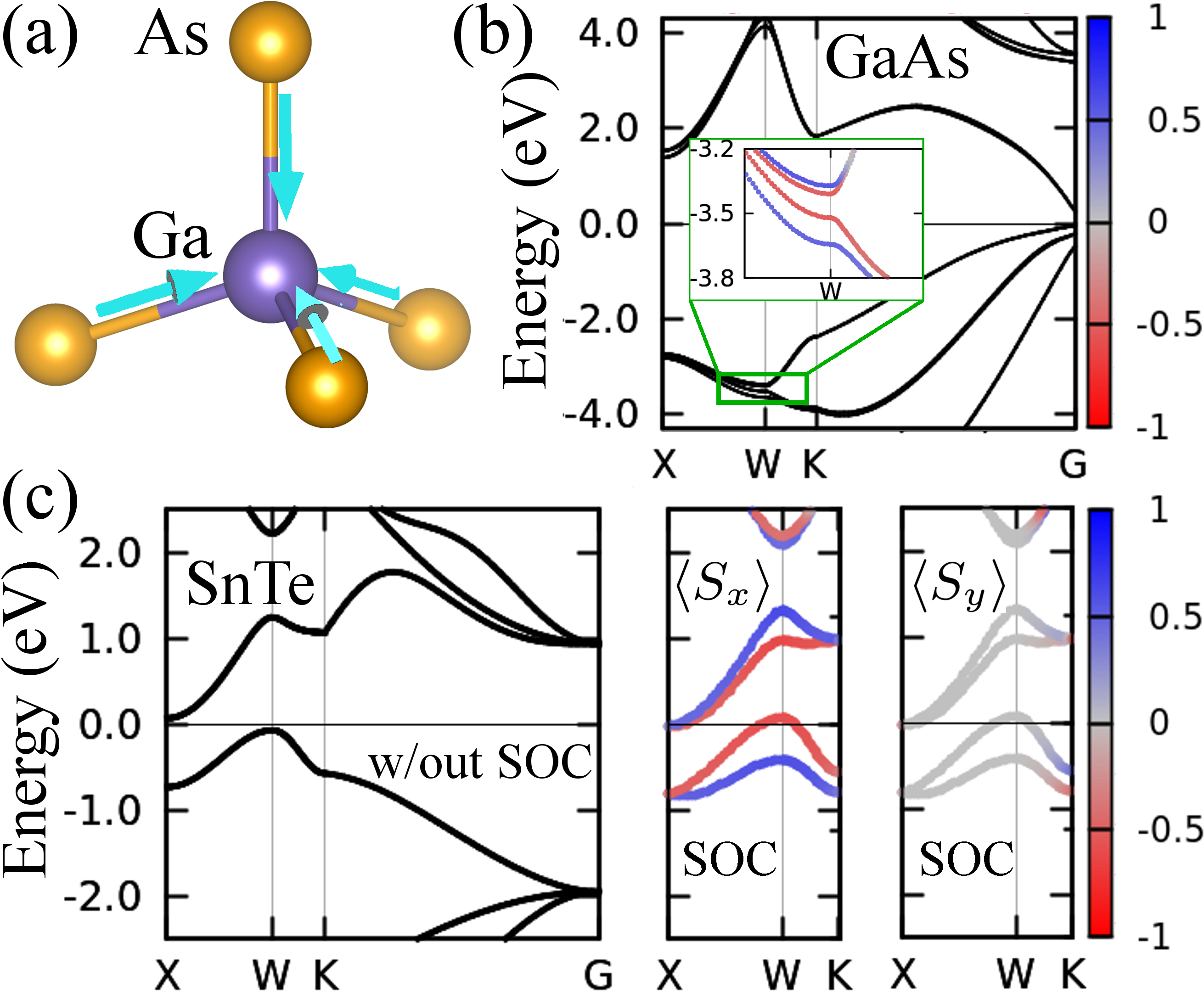 Figure 1
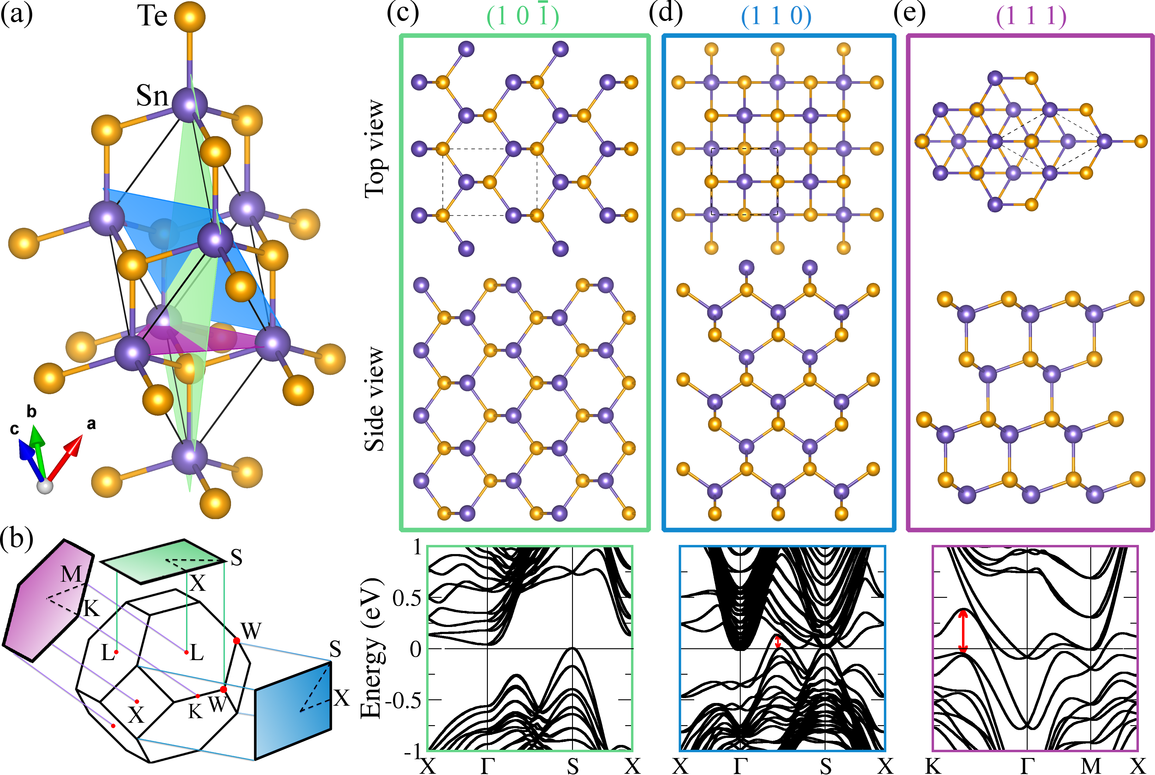 Figure 2
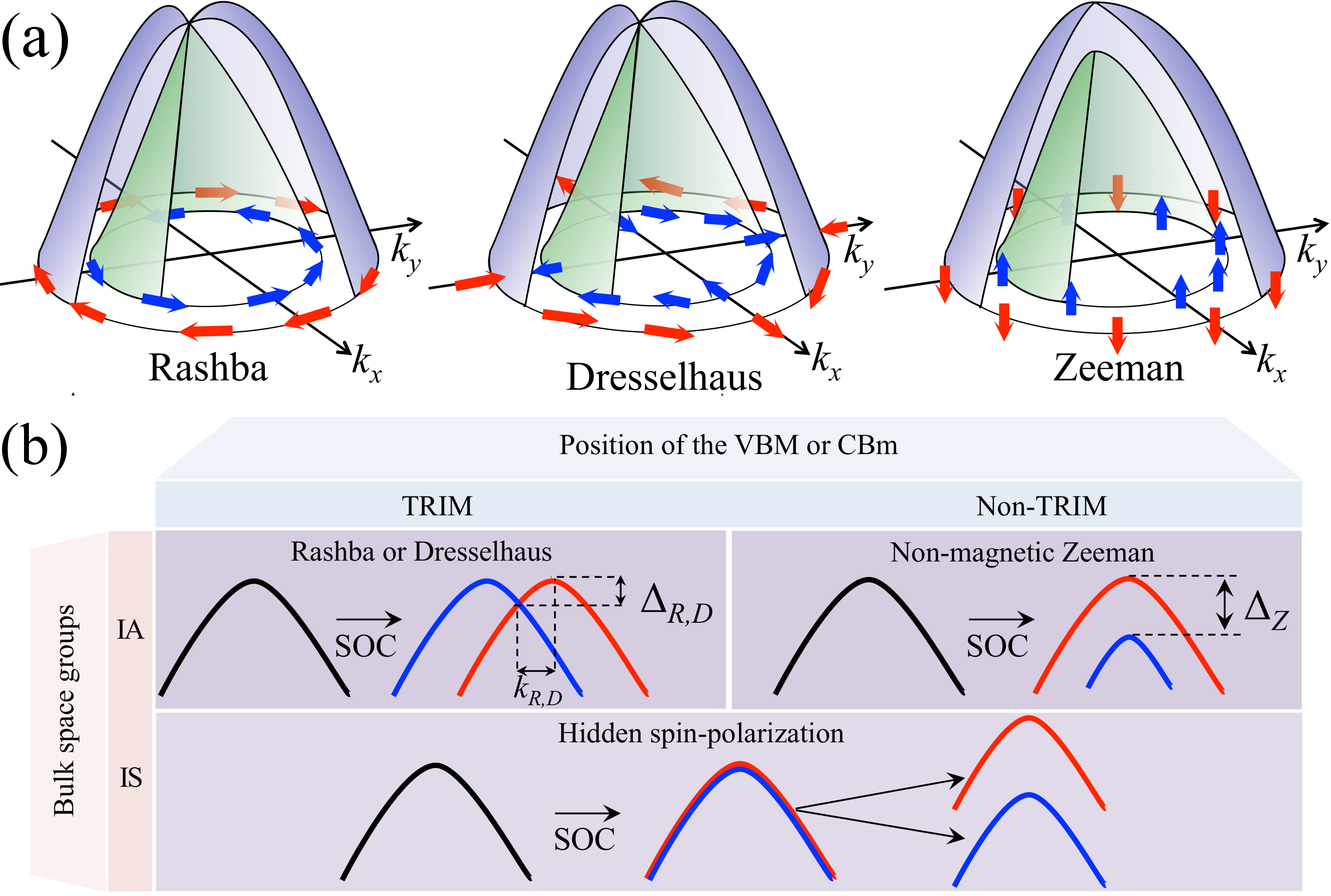 Figure 3
| Compound | (meV) | (meV) | (eV) | (eV) | (eV) | Space group | Exp. | Theory | ICSD code |
| Ge3As4 | 13 | – | 0.005 | 0.05 | 0.155 | P3m | – | [31] | 163833 |
| SnS | 49 | – | -0.495 | 0.28 | 0.166 | F3m | [32] | [29] | 43409 |
| OsC | 332 | 340 | 0.772 | 0.772 | 0.279 | P213 | – | [33] | 168277 |
| Mn2Ge | 192 | 141 | 0.137 | 0.253 | 0.132 | F3m | [34] | – | 184947 |
| RuGe | 97 | 101 | -0.281 | 0.013 | 0.185 | P213 | [35] | – | 637744 |
| OsSi | 346 | 202 | -0.367 | 0.012 | 0.512 | P213 | [36] | – | 647777 |
| FeSi | 70 | 17 | -0.511 | 0 | 0.181 | P213 | [37, 38, 39] | – | 633542 |
| RuSi | 85 | 81 | -0.647 | 0 | 0.261 | P213 | [40, 41, 42] | – | 85209 |
| WSi2 | – | 38 | -0.277 | 0.066 | 0.034 | P22 | [43, 44] | – | 652549 |
| WN2 | 433 | 125 | -0.521 | 0 | 1.070 | Pm2 | – | [45] | 290433 |
| Bi2O3 | – | 81 | -1.562 | 0.092 | 2.416 | R3m | – | [46] | 168810 |
| MoS2 | 187 | – | -1.303 | 0.003 | 1.422 | R3m | [47, 48, 49] | – | 43560 |
| WS2 | 510 | – | -1.26 | 0.004 | 1.841 | R3m | [50, 51] | – | 202367 |
| Ir4Ge5 | 16 | – | -0.34 | 0 | 0.128 | Pc2 | [52, 53, 54] | – | 42909 |
| Tl2Te3 | 156 | 197 | -0.167 | 0.024 | 0.445 | Cc | [55] | – | 26282 |
| GeO2 | 7 | – | -0.533 | 1.561 | 0.985 | P3 | [56] | – | 53869 |
| SnTe | 491 | – | -0.034 | 0.252 | 0.240 | F3m | [28] | – | 53956 |
| Bi2O3 | 15 | – | -1.486 | 0.168 | 0.149 | Pm2 | – | [46] | 168808 |
| In2Te5 | – | 31 | -0.233 | 0 | 1.041 | Cc | [57, 58] | – | 640615 |
| Cs2Te3 | 53 | 209 | -0.755 | 0 | 0.637 | Cmc21 | [59, 60] | – | 53245 |
Peer Reviews
No public reviews on file for this paper yet. If you reviewed it on a platform where reviews are public (OpenReview, ICLR, NeurIPS, ICML), you can paste yours below so the community can read it here.
Videos
No videos yet. Explain this paper in a talk, walkthrough, or lecture? Add one.
Taxonomy
TopicsElectronic and Structural Properties of Oxides · Quantum and electron transport phenomena · Advanced Condensed Matter Physics
Zeeman-type spin splitting in non-magnetic three-dimensional compounds: Materials prediction and electrical control
Carlos Mera Acosta
Center of Natural and Human Sciences, Federal University of ABC, 09210-580, Santo André, SP, Brazil
Brazilian Nanotechnology National Laboratory, CP 6192, 13083-970, Campinas, SP, Brazil
Adalberto Fazzio
Center of Natural and Human Sciences, Federal University of ABC, 09210-580, Santo André, SP, Brazil
Brazilian Nanotechnology National Laboratory, CP 6192, 13083-970, Campinas, SP, Brazil
Gustavo M. Dalpian
Center of Natural and Human Sciences, Federal University of ABC, 09210-580, Santo André, SP, Brazil
Abstract
Despite its potential for device application, the non-magnetic Zeeman effect has only been predicted and observed in two-dimensional compounds. We demonstrate that non-centrosymmetric three-dimensional compounds can also exhibit a Zeeman-type spin splitting, allowing the splitting control by changing the growth direction of slabs formed by these compounds. We determine the required conditions for this effect: i) non-centrosymmetric including polar and non-polar point groups, ii) valence band maximum or conduction band minimum in a generic -point, i.e., non-time-reversal-invariant momentum, and iii) zero magnetic moment. Using these conditions as filters, we perform a material screening to systematically search for these systems in the aflow-ICSD database. We find 20 material candidates featuring the Zeeman-type effect. We also found that the spin-splitting in confined systems can be controlled by an external electric field, which in turns can induce a metal-insulator transition. We believe that the Zeeman-type effect in three-dimensional compounds can potentially be used for spin-filtering devices.
The manipulation of inversion and time-reversal (TR) symmetries have been the cornerstone of novel phenomena allowing the generation and control of spin-polarized states in crystalline materials, the principal goal of spintronics [1, 2, 3, 4]. The TR-symmetry breaking, which is usually induced by external magnetic fields or the intrinsic magnetic order, can lead to a separation in energy of bands with opposite spin, i.e., Zeeman spin splitting [5, 6, 7]. In non-magnetic compounds, the combination of the atomic-site polarity and bulk point group results in all possible structural configurations leading to intrinsic spin-polarized states [8, 9, 10]. For instance, in bulk inversion asymmetry (IA) materials, the spin-polarization is always accompanied by a spin splitting typically referred to as either Dresselhaus [11] or Rashba effect [12, 13] according to the spin-texture orientation (see Fig. 1a). The split-bands have the opposite helical in-plane spin-texture in Rashba semiconductors and the same helicity in band inverted Rashba semiconductors [14]. In the Dresselhaus effect, the spin-polarization is parallel to () for and . The band dispersion curves related to these effects, which are represented in Fig. 1b, have been characterized by spectroscopic measurements for many surfaces and interfaces [15, 16, 17, 18], and can be described by a simplified Hamiltonian model,
[TABLE]
where , is the spin-orbit coupling (SOC) field, and are the Pauli matrices. Here, , is the effective mass of electrons, and is the 22 unitary matrix. The specific form of depends on the material symmetry [19, 20]. For instance, in a two-dimensional system with point group, the Rashba and Dresselhaus fields are written as and , respectively. The strength of the Rashba (Dresselhaus) field is given by the parameter (). The parameter is different from zero in systems featuring a non-zero electric dipole [21], which can be intrinsic or, as originally proposed by Rashba, induced by interfacing semiconductors or external electric fields. The Rashba effect is typically used for the electrical control of the spin-polarization [2, 3, 4, 22]. For these reasons, IA materials have historically been the most promissory candidates for spintronic devices.
Besides the Rashba and Dresselhaus effects, another kind of spin splitting in non-magnetic IA compounds, whose spin texture is similar to the one observed in the magnetic Zeeman effect, is the so-called Zeeman-type spin splitting (See Fig. 1a). Despite its potential for device application, this non-magnetic effect has only been predicted and observed in the two-dimensional WSe2 and MoS2 [23, 24, 25]. Unlike the Rashba and Dresselhaus splitting, the Zeeman-type splitting does not have a band crossing (See Fig. 1a) and has been related to the effect of an electric dipole or an external electric field [23]. This suggests that this effect can only be induced in two-dimensional systems. Indeed, it has not been explored in three-dimensional compounds.
Here, we demonstrate that IA three-dimensional compounds can also exhibit a Zeeman-type spin splitting, allowing the splitting control by changing the growth direction of slabs formed by these compounds. For this purpose, we first establish the conditions for non-magnetic spin-split bands. Using these conditions as filters, we perform a material screening in the AFLOW-ICSD database [26, 27], i.e., a systematic search of fabricated materials. We find 20 binary three-dimensional compounds featuring the Zeeman-type effect. Aside from the prediction of large Zeeman splitting in the three-dimensional version of layered systems exhibiting this effect (the VBM in MoS2 and WS2 have a spin splitting of 187 and 510 meV, respectively), we also find large spin splitting in compounds that are not formed by van der Waals (vdW) layered materials, such as, OsC, WN2, and SnTe, with splittings between 330 and 490 meV. A representative example of these non-magnetic Zeeman materials is the SnTe compound stabilizing the Zinc-Blende (ZB) structure [28]. We confirm that in the SnTe slab, the Zeeman-type splitting depends on the growth direction, suggesting that the total electric dipole is modified by the surface induced dipole. Based on this, we then propose the electrical control of the Zeeman-type effect. We believe that this work will open the way for the discovery of novel fundamental effects related to the spin-polarization control.
Results
Design principles and materials screening
Based on the space group and chemical composition analyzes, we determine the conditions that a material should meet to exhibit the Zeeman-type effect. Design principles are typically used as filters to predict or select compounds from the materials databases [61], e.g., AFLOW [26, 27] and materials project [29, 30]. By combining the materials screening with high-throughput density functional theory calculations (See section Methods), we have an efficient approach to predict novel Zeeman-type semiconductors.
The Zeeman-type effect is the spin discrimination as a consequence of the inversion-symmetry (IS) breaking at non-TR invariant -points, rather than the effect of an intrinsic electric dipole, as we discuss below. We then define the conditions that a material should satisfy to exhibit the Zeeman-type effect: i) inversion-assymetry (IA) and TR symmetry (non-centrosymmetric bulk and non-magnetic moment), ii) a total electric dipole is not needed (polar and non-polar point groups), and iii) the VBM and CBM must take place at a non-TR-invariant -point. These conditions are summarized in Fig. 1b. Specifically, the Zeeman-type splitting is related to non-centrosymmetric non-magnetic materials, i.e., only compounds with bulk point groups , , (with and ), , , , , , , and could feature the non-magnetic Zeeman effect. When the VBM or CBM take place at a TR-invariant -point, the compounds are classified as a Rashba or Dresselhaus semiconductors (See Fig. 1b). Additionally, compounds in other symmetries could feature the hidden-spin-polarization, as represented in Fig. 1b.
We use the previously established conditions as filters for a systematic search of non-magnetic Zeeman materials. We perform a materials screening in the AFLOW-ICSD database [26, 27], which contains information of approximately 59000 fabricated materials. After eliminating compounds with the same formula, space group, and the number of atoms in the unit cell, we obtain 32553 entries. There are 8360 binary compounds, which in turn can be divided into 1326 IA and 7034 IS materials. Among the IA compounds, we find 587 non-magnetic gaped and 739 gapless magnetic materials. Finally, only 20 non-magnetic IA compounds exhibit either the CBM or the VBM at non-TR-invariant -points. Detailed information of the predicted Zeeman-type materials is presented in Table 1.
Some materials in the ICSD-database have been fabricated under specific conditions of pressure and temperature, therefore, these compounds could be above the boundary of the convex-Hull, i.e., the phase diagram representing the set of lowest possible potential energy states obtained from both single materials and mixtures of those materials. Remarkably, in the selected compounds, we find systems forming the boundary of the convex-Hull (), suggesting that they are in the most stable structural configuration, such as, WN2 and RuSi, FeSi, Ir4Ge5, In2Te5, and Cs2Te3 in the space groups Pm2, P213, P213, Pc2, Cc, and Cmc21, respectively. We find that for RuGe, OsSi, MoS2, WS2, and Tl2Te3 the energy above the convex Hull is less than 30 meV/atom, which means that these materials could be easily synthesized.
For WS2 and MoS2 (space group ), the bulk is centrosymmetric and the site point group and of the Mo and S atoms are non-centrosymmetric, which results in a hidden Dresselhaus spin-polarization [23, 25]. However, in the non-centrosymmetric space group , the VBM of these materials has a giant Zeeman-type splitting about 510 and 187 meV, as shown in Table 1. We also find that compounds with the same formula but with different structure could exhibit different splitting values. For instance, Bi2O3 (space group ) has a splitting of 81 meV in the CBM, whereas the VBM of this compound in the space group has a splitting of 15 meV. This is expected since the on-site SOC is not the unique property related to the spin splitting [21]. Indeed, systems formed by atoms with a relatively weak SOC could also have large splitting values, e.g., meV in Mn2Ge.
Surfaces and electrical control
Since surfaces and two-dimensional confinement affect the symmetry and the total electric dipole, we here explore the spin splitting in the surfaces of Zeeman-type semiconductors and its possible electrical control. For illustrative purposes, we will present here the results for the SnTe (one of the materials with the largest splitting). We consider three growth directions corresponding to planes parallel, oblique, and perpendicular to the Sn-Te bonding along the axis normal to the surface (111) (See Fig. 2a), i.e., planes at the crystallographic directions (10), (110), and (111), respectively. We find that the spin splitting change according to the growth direction of the slab. Specifically, the splitting is near zero for the plane (10) and increases as the angle between the plane and the bonding increases. Thus, the (110) and (111) planes exhibit a splitting of 50 and 491 meV (See Fig. 2c-e). Consequently, the slab (10) is an insulator, whereas the (110) and (111) surfaces are metallic. This insulator-metal transition are a remarkable effect arising from large spin splittings in non-magnetic Zeeman semiconductors. If the spin splitting in the VBM is greater than the bandgap, the highest energy band can cross the Fermi energy, leading to majority spin channels, as shown for SnTe in Fig. 2c-e. This transition can be induced and controlled in a specific slab by manipulating the Zeeman splitting, which can be used for application in spintronics, e.g., spin filtering. For instance, a perpendicular external electric field could modify the electric dipole induced by the surface. For SnTe slab along the (111) surface, an applied electric field decreases the spin splitting, leading to a metal-insulator transition for eV/Å. By increasing the electric field, the bandgap opens again due to the change on the electric dipole orientation, resulting in an insulator-metal transition for eV/Å.
Discussion
The Zeeman-type splitting in the so far proposed layered materials has been interpreted in terms of a non-zero intrinsic dipole [23]. This interpretation, based on the common understanding of the Rashba effect, implies that compounds in which the atomic dipoles add up to zero, e.g., ZB GaAs, cannot exhibit this splitting, which is not necessarily correct, as we discuss below. A historical example of Dresselhaus semiconductors is the GaAs (space group F3m). In this IA compound, the dipoles add up to zero due to the tetrahedral chemical environment imposed by the crystal symmetry, as represented in Fig. 3a. Thus, although the Rashba terms do not contribute to the Hamiltonian describing the GaAs band structure, the spin splitting reaches high values () at the high symmetry point W (See Fig. 3b), as early reported in Ref. [62]. On the other hand, for ZB binary semiconductors, the position of the CBM and VBM can change according to the chemical composition (AB) [63]: GaAs and Germanium have a direct band gap at , but in Silicon and GaP, the CBM is at the X point. Here, we find that the VBM can take place at the W point (highest spin splitting in GaAs) for A=Sn and B=Te, as represented in Fig. 3c. Naturally, SnTe has also a zero internal dipole, but a giant spin Zeeman-type splitting of 491 meV (See Table 1). States exhibiting large spin-splitting can be brought up to the Fermi energy by changing the atomic composition, as evident from the predicted compounds. This can be a different route to find this kind of materials, which typically exhibit splittings larger than the the observed in the Rashba and Dresselhaus effects, as we demonstrate below.
In ZB semiconductors, the spin-polarized states near the point are described by the Eq. 1 with and the effective Rashba and Dresselhaus fields given by and , respectively. Here, is a unitary vector along the direction of the electric dipole. Accordingly, the spin-splitting generated by these odd-in- effective magnetic fields is
[TABLE]
where and are the eigenvalues of the Hamiltonian . In order to show that the Zeeman splitting is typically larger than the Rashba and Dresselhaus splitting, we consider an illustrative case: and . Thus, the spin-splitting becomes . In the Rashba effect, the momentum offset usually reaches small values between 10 and 10 (See Fig. 1b) [3]. Therefore, although the parameter may be large (), the splitting values are always limited to some meV [3, 15, 16, 17, 18]. This is also valid in compounds in which the atomic dipoles add up to zero, where and . Since the non-TR-invariant high symmetry -points are at the boundary of the BZ, Zeeman-type splitting are always larger than Rashba and Dresselhaus splitting. Additionally, due to the spin splitting position in the BZ, the Zeeman-type effect offers alternative mechanisms for spin polarization control.
Along the X-W symmetry line, the spin-texture of the SnTe band structure is dominated by spin components. This can be verified form the Hamiltonian for . Because along such direction and , the Dresselhaus field can be written as . Therefore, the splitting can be controlled by changing the growth direction of slabs. For instance, when the systems are confined along the (10), we can write . Consequently, the Zeeman spin splitting at the W-point (S-point in the equivalent two-dimensional BZ, as shown in Fig. 2b) vanishes.
Different from the Rashba and Dresselhaus splitting at TR-invariant -points, the non-magnetic Zeeman effect does not allow the spin-polarization electrical control, but the spin-filtering effect mediated by the electrical control of the splitting size. Specifically, an external electric field does not change the spin-polarization, but the splitting size. The electric field can then bring states with a specific spin to the Fermi energy. This control mechanism is different from the recently reported in the magnetic-Zeeman splitting [64]. As previously discussed, the electrical control of the spin splitting can also be achieved in these materials according to the growth direction of the slab.
In conclusion, we demonstrate that IA three-dimensional non-magnetic compounds can exhibit a Zeeman-type spin splitting, providing the possibility to grow slabs in which the electrical dipole is perpendicular to the surface and hence, allowing the electrical control of the spin splitting. The required conditions for this effect are: valence band maximum or conduction band minimum in a non-time-reversal-invariant k-point, inversion asymmetry, and zero magnetic moment. Using these conditions as filters, we perform a material screening and high-throughput ab-initio calculations to systematically search for these materials in the aflow-ICSD database. We find 20 candidates featuring this splitting. Our calculated spin splittings can be as large as 433, 510, and 491meV for the compounds WN2 (P6m1), WS2 (R3m), and SnTe (F43m), respectively. We also demonstrate that the spin splitting in slabs of these compounds depends on the growth direction and can be controlled by an external electric field. We believe that this work will open the way for the discovery of novel fundamental effect related to the spin-polarization control.
Methods
The ab initio calculations were performed within the density functional theory (DFT) using Perdew-Burke-Ernzenhof generalized gradient approximation (PBE) [65] exchange-correlation functional and the Hubbard on-site term [66, 67] as implemented in the Vienna Ab-initio Simulation Package (VASP) [68, 69]. All the specific settings of the calculations without spin-orbit coupling (e.g. cutoff energies, k-point sampling, effective U parameters, atomic configurations) were the same as to those used on the AFLOW database [26, 27]. We have then included the spin-orbit interaction keeping the zero magnetic moment.
Acknowledgements
This work was financed by FAPESP (grants 18/11856-7 and 17/02317-2), and CNPq. This work was performed using the computational infrastructure of the LNCC supercomputer center (Santos Dumont).
The reference list from the paper itself. Each links out to its DOI / PubMed record.
- 1[1] Jansen, R. Silicon spintronics. \Journal Title Nat Mater 11 , 400–408 (2012). URL http://dx.doi.org/10.1038/nmat 3293 . DOI 10.1038/nmat 3293. · doi ↗
- 2[2] Maekawa, S., Valenzuela, S. O., Saitoh, E. & Kimura, T. Spin Current (Series on Semiconductor Science and Technology 17, Oxford University Pres, 2012).
- 3[3] Manchon, A., Koo, H. C., Nitta, J., Frolov, S. M. & Duine, R. A. New perspectives for rashba spin-orbit coupling. \Journal Title Nat Mater 14 , 871–882 (2015). URL http://dx.doi.org/10.1038/nmat 4360 . · doi ↗
- 4[4] Bercioux, D. & Lucignano, P. Quantum transport in rashba spin–orbit materials: a review. \Journal Title Reports on Progress in Physics 78 , 106001 (2015). URL http://stacks.iop.org/0034-4885/78/i=10/a=106001 .
- 5[5] Zeeman, P. The effect of magnetisation on the nature of light emitted by a substance. \Journal Title Nature 55 , 347 EP – (1897). URL http://dx.doi.org/10.1038/055347 a 0 . · doi ↗
- 6[6] Preston, T. Radiation phenomena in the magnetic field. \Journal Title Nature 59 , 224 EP – (1899). URL http://dx.doi.org/10.1038/059224 c 0 . · doi ↗
- 7[7] Li, Y. et al. Valley splitting and polarization by the zeeman effect in monolayer mose 2 subscript mose 2 {\mathrm{mose}}_{2} . \Journal Title Phys. Rev. Lett. 113 , 266804 (2014). URL https://link.aps.org/doi/10.1103/Phys Rev Lett.113.266804 . DOI 10.1103/Phys Rev Lett.113.266804.
- 8[8] Zhang, X., Liu, Q., Luo, J.-W., Freeman, A. J. & Zunger, A. Hidden spin polarization in inversion-symmetric bulk crystals. \Journal Title Nature Physics 10 , 387 EP – (2014). URL http://dx.doi.org/10.1038/nphys 2933 . · doi ↗