Single charge transport in a fully superconducting SQUISET locally tuned by self-inductance effects
Emanuele Enrico, Luca Croin, Elia Strambini, Francesco Giazotto

TL;DR
This paper introduces a fully superconducting SQUISET device that uses self-inductance effects for local, independent control of charge states and conductance, enhancing single-electron manipulation and magnetic flux sensing capabilities.
Contribution
The work demonstrates a novel fully superconducting SQUISET with independently tunable charge and conductance via self-inductance, improving device flexibility and control.
Findings
Sensitive to single charge states and magnetic fields
Robust modulation of current-to-flux transfer function
Independent control of conductance in nano-engineered junctions
Abstract
We present a single-electron device for the manipulation of charge states via quantum interference in nanostructured electrodes. Via self-inductance effects, we induce two independent magnetic fluxes in the electrodes and we demonstrate sensitivity to single charge states and magnetic field at variable temperature. Moreover, our approach allows us to demonstrate local and independent control of the single-particle conductance between nano-engineered tunnel junctions in a fully-Superconducting Quantum Interference Single-Electron Transistor (SQUISET), thereby increasing the flexibility of our single-electron transistors. Our devices show a robust modulation of the current-to-flux transfer function via control currents, while exploiting the single-electron filling of a mesoscopic superconducting island. Further applications of the device concept to single-charge manipulation and…
Click any figure to enlarge with its caption.
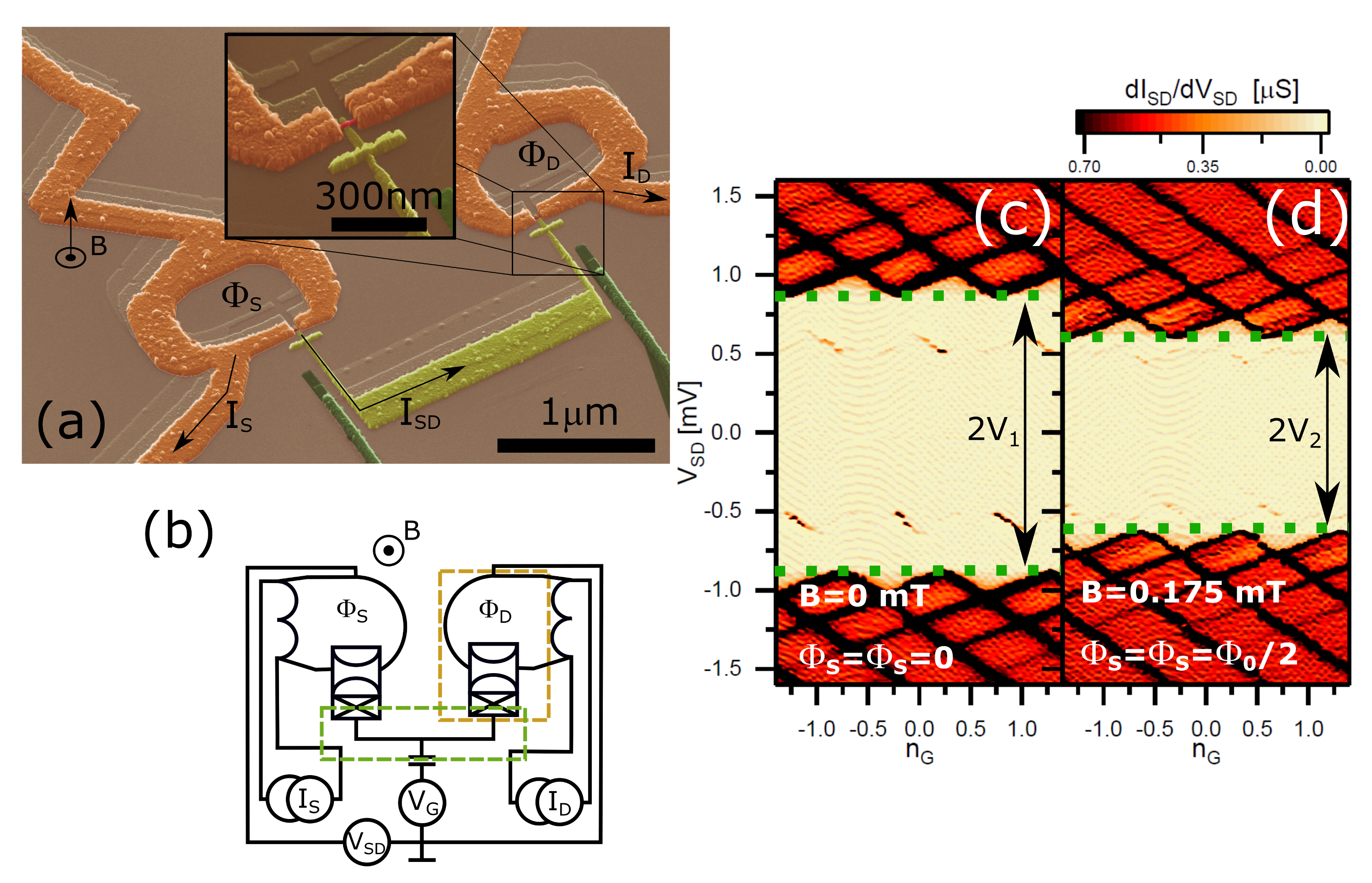 Figure 1
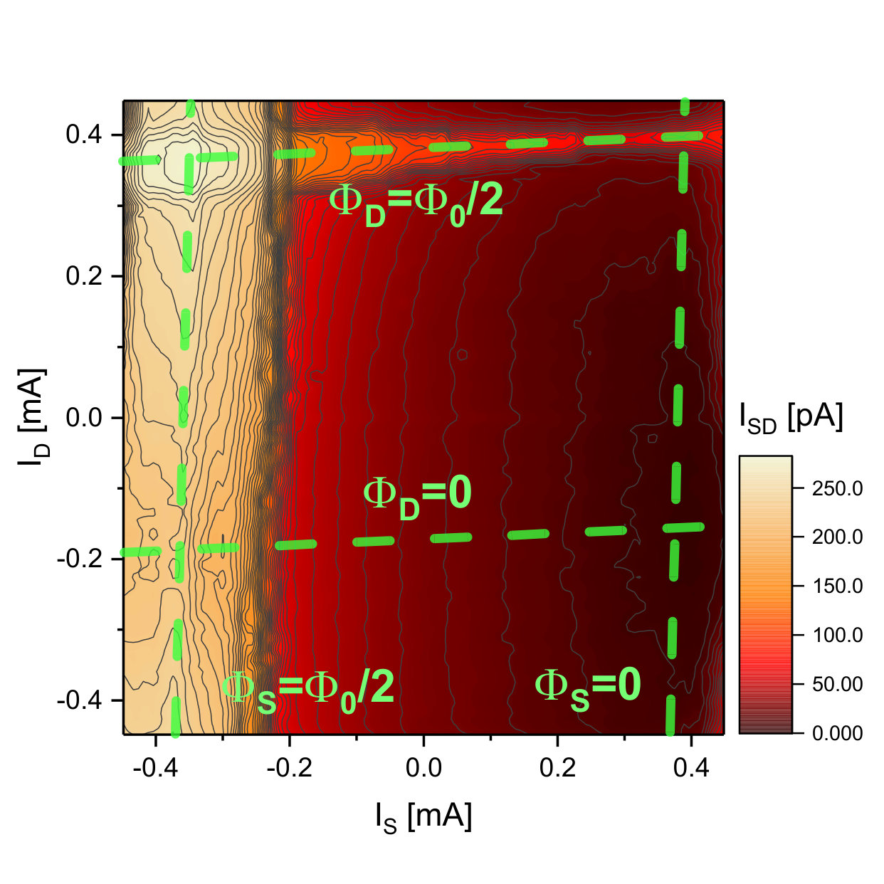 Figure 2
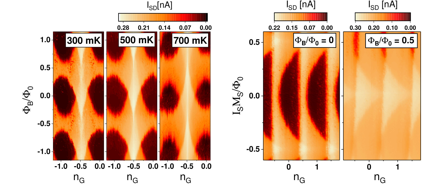 Figure 3
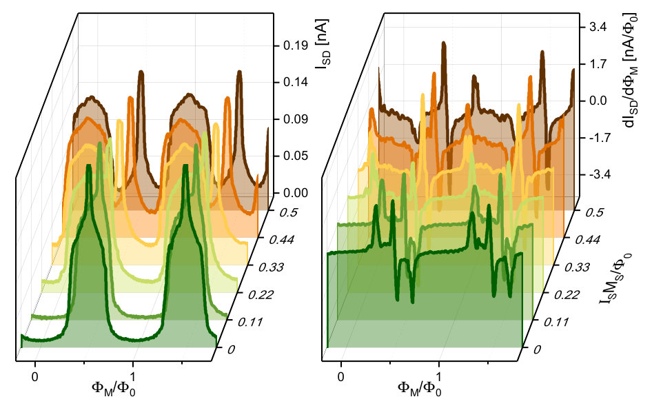 Figure 4
Peer Reviews
No public reviews on file for this paper yet. If you reviewed it on a platform where reviews are public (OpenReview, ICLR, NeurIPS, ICML), you can paste yours below so the community can read it here.
Videos
No videos yet. Explain this paper in a talk, walkthrough, or lecture? Add one.
Single charge transport in a fully superconducting SQUISET locally tuned by self-inductance effects
E. Enrico
L. Croin
INRIM, Istituto Nazionale di Ricerca Metrologica, Strada delle Cacce 91, I-10135 Torino, Italy
E. Strambini
F. Giazotto
NEST, Istituto Nanoscienze-CNR and Scuola Normale Superiore, Piazza S. Silvestro 12, Pisa I-56127, Italy
Abstract
We present a single-electron device for the manipulation of charge states via quantum interference in nanostructured electrodes. Via self-inductance effects, we induce two independent magnetic fluxes in the electrodes and we demonstrate sensitivity to single charge states and magnetic field at variable temperature. Moreover, our approach allows us to demonstrate local and independent control of the single-particle conductance between nano-engineered tunnel junctions in a fully-Superconducting Quantum Interference Single-Electron Transistor (SQUISET), thereby increasing the flexibility of our single-electron transistors. Our devices show a robust modulation of the current-to-flux transfer function via control currents, while exploiting the single-electron filling of a mesoscopic superconducting island. Further applications of the device concept to single-charge manipulation and magnetic-flux sensing are also discussed.
††preprint: AIP/123-QED
Superconducting nanoelectronics has continuously grown in the last decades as a flexible and promising platform for the implementation of quantum-based sensorsGiazotto et al. (2010); Ronzani et al. (2017); D’Ambrosio et al. (2015) and quantum-states manipulating circuitsUri and Michel ; Strambini et al. (2016), with particular attention to interference-based superconducting devicesVirtanen, Ronzani, and Giazotto (2016) and mesoscopic structures where single charges play dominant rolesEnrico and Giazotto (2016); Enrico, Strambini, and Giazotto (2017). Different geometries can be easily combined with standard nanolithography techniquesFulton and Dolan (1987), opening the field to complex and robust devices embedding multiple control lines and tunable working points in the parameters space. As a consequence, superconducting nanoelectronics technology represents an exceptional research platform for condensed-matter quantum physics experiments as well as for scalable quantum computingClarke and Wilhelm (2008) and photonics applicationsGu et al. (2017).
Normal-metalPothier et al. (1992), hybridPekola et al. (2007) or fully-superconductingAverin and Nazarov (1992) single-electron devices - fabricated by shadow-mask technique Fulton and Dolan (1987) - have been so far one of the research topics where nanofabrication technology excelled, leading to device concepts where the detection of charge states approaching their coherent superpositionNakamura, Pashkin, and Tsai (1999) has been routinely reached. While rather complex single-electron systems based on local electrical gating have been demonstratedMartinis, Nahum, and Jensen (1994), the on-chip tunability of their electrodes carriers population has been limited to the semiconductor nanowiresHollosy et al. (2015) and the 2D-electron-gas based technologiesGiblin et al. (2012), where clear manipulation of Coulomb blockade effects has only been allowed via strong electric fields.
Nano-engineered superconducting electrodesEnrico, Strambini, and Giazotto (2017) introduce an alternative control parameter, the magnetic flux, that can act on the population of quasiparticles charge carriersManninen et al. (1999) via quantum interferenceGiazotto et al. (2010). Short metallic nanowires have been embedded in superconducting loops Enrico and Giazotto (2016) leaving enough space to be coupled to a Coulombic island through mesoscopic tunnel junctions. The present technology, which is mostly based on aluminum tunnel junctions, is then further extended by an unprecedented level of control and flexibility offered by localized magnetic fluxes. Various approaches exploiting these phenomena demonstrated state-of-the-art magnetic flux sensing capabilitiesLigato et al. (2017); Ronzani et al. (2017); D’Ambrosio et al. (2015) and single charges states manipulationEnrico, Strambini, and Giazotto (2017) but still lack for on-chip control.
Here we demonstrate that two local magnetic fluxes can be used to manipulate the electrodes density of states of a fully superconducting SQUISET and to efficiently modify its electron transport properties. In particular, we show how the typical Coulomb energy of the island can be controlled by the quasiparticle spectra of the source and drain electrodes by exploiting self-inductance effects.
A prototypical device is depicted in Figure 1. A superconducting island is connected to the source and drain electrodes via tunnel junctions. Both source and drain consist of a superconducting nanowire embedded in a superconducting loop. Each ring has two contact pads for the injection of the source-drain current and the currents for the independent control of the fluxes. The entire structure is realized via three-angle-deposition (//) of aluminum (//) through a suspended mask on a Si/SiO2 ( thick oxide) substrate (see Figure 1a). The polymeric mask has been obtained via electron beam lithography, whereas thin films deposition has been performed via electron beam evaporation. Tunnel junctions were created between the first and the second deposition step by oxygen exposure ( for ). One of the tunnel junction across the nanowire and the island is visible in the inset of Figure 1a. The device configuration defines three main current path , and . The first two act as control currents flowing along parts of the source and drain loops, while the last is the effective current flowing through the Coulombic island (Figure 1b). The entire chip is pierced by an uniform magnetic field, , generated by an external magnet inducing a flux in both the identical loops of area . The combined effect of and the local currents gives rise to two magnetic fluxes at the source ad drain loops, and , respectively. and are the self-inductances while and are the mutual inductances between opposite loop. The electrodes are biased via an external voltage source (), and the island is exposed to a control electric field via a capacitively-coupled gate that induces quantized charges, being the gate-island capacitance, the gate voltage and the electron charge. This device architecture is designed to act essentially as a fully superconducting single electron transistorNakamura, Sakamoto, and Tsai (1995); Nakamura, Chen, and Tsai (1996) with two identical tunnel junctions (total series resistance R_{T}\approx$$1.75\text{\,}\mathrm{M\SIUnitSymbolOhm}). In the absence of a magnetic field, this is confirmed by the differential conductance stability diagram in Figure 1c clearly showing the effect of the charging energy, evaluated to be E_{C}=$$75\text{\,}\mathrm{\SIUnitSymbolMicro eV} from the Coulomb diamonds and confirmed by the Josephson-quasiparticle peaks (JQPs)Nakamura, Chen, and Tsai (1996); Korotkov (1996); Fulton et al. (1989); van den Brink, Schön, and Geerligs (1991); Averin and Nazarov (1992). In particular, dark and sharp JQPs conductance peaks clearly visible in the blocked region of Figures 1c and 1d result to be unaffected by the small magnetic field applied since they depend on the island superconducting gap and only. Therefore, from the JQPs we have estimated \Delta_{I}\approx$$216\text{\,}\mathrm{\SIUnitSymbolMicro eV}. When the SQUISET is uniformly pierced by , the condition can be reached, as show in Figure 1d, and the superconducting gaps of the the two nanowires are reduced to their minimum via quantum interference. This effect can be appreciated by the reduction of the voltage threshold separating the conducting region, where the transport is dominated by quasiparticles tunneling and not JQP cycles, respect the blocked one ( in Figure 1c and in Figure 1d). It’s worth mentioning here that and have been selected as reference thresholds, for which the independence by the charging energy is guaranteed by their position respect the coulomb diamonds. From there, the zero magnetic field and the superconducting gaps of the electrodes have been deduced (\Delta_{S,0}=\Delta_{D,0}\approx$$235\text{\,}\mathrm{\SIUnitSymbolMicro eV} and \Delta_{S,1/2}=\Delta_{D,1/2}\approx$$84\text{\,}\mathrm{\SIUnitSymbolMicro eV}).
The effect of local magnetic flux biasing via and is shown in Figure 2, where the source-drain current is monitored at fixed bias as a functions of the currents flowing in the loops. The non-symmetrical behavior shown in Figure 2 suggests an asymmetry in the dynamical conductance of the two tunnel junction involved. From the analysis of maxima and minima fitted positions in this diagram, represented by quasi-orthogonal light green dashed lines, it is possible to observe and quantify the effect of the self-inductances, giving M_{S}=0.69\Phi_{0}/$$\mathrm{mA} and M_{D}=0.87\Phi_{0}/$$\mathrm{mA}. From these estimates, the cross-influence of the flux control lines turns out to be almost negligible (m_{S,D}<0.05\Phi_{0}/$$\mathrm{mA}) and the electrodes quasiparticles density of states results to be almost independently tunable by and , respectively. In order to further investigate the effect of an independent flux biasing via local effects, we have performed a temperature series measurements that confirm the single-charge sensitivity of our device up to T=$$700\text{\,}\mathrm{mK} (Figure 3(a)). There, a symmetrical magnetic flux biasing condition via respects the periodical modulation of the source-drain current when the device is biased at . It’s worth mentioning that experimental data reported in Figure 3 are affected by unavoidable background charge as commonly happens in single-charge sensitive devices. These offsets where removed by referring to the normalized quantized induced charge value, whose zero is centered in one of the minima. By exploiting this evidence, we proceeded investigating the effect of local magnetic and electrical gating at T=$$700\text{\,}\mathrm{mK} and two different magnetic field leading to and (see Figure 3(b)). There, the periodical and asymmetrical dependence of on reflects the unbalanced condition of the electrodes superconducting gaps that affects the conductances of the tunnel junctions, with clear similarities to the behavior reported in Figure 3(a). Triangular regions in the - plane, corresponding to maximum current, are shifted and expanded from the condition (when no external magnetic field is applied) to when a uniform magnetic flux offset is introduced (). Analogously, semi-circular regions corresponding to blockaded regions of almost zero current are shrunk and shifted around the condition. The mechanism of unbalanced response to magnetic field is analyzed in detail in Figure 4(a), where we report the evolution of the flux-modulated current () at different . presents sharp and periodic peaks on top of broader peaks. These latter are controlled by which induces their gradual separation. Yet, the sharp structures depends only on , while their sharpness stems from the asymmetry existing between local conductances of the source and drain tunnel junctions Fasolo, Borchia, and Enrico (2021). The S’ISIS” structure of our device expresses here strong asymmetrical behavior respect the the symmetrical geometry, simply due to the local action of unbalancing flux given by self-inductance effects. Sharp peaks at are independent respect the current and can be attributed to the island-drain junction, confirming the negligible correlation between the two flux control lines of our device. The wider plateau of can be shifted along the axis at will by acting on the current. These plateau are clearly wider respect the sharp peaks of the island-drain junction due to the asymmetric voltage bias of the circuit (see Figure 1(b)). In order to quantify the flux-to-current transfer function we show in Figure 4(b) the numerical derivative of respect to . Double peaked transfer functions reflect the role of the two different superconducting gaps, moreover the effect of the flux bias via can be exploited to further increment the responsiveness of our device to magnetic flux variation. As an example, when the two negative peaks collapse in one and effectively enhance the transfer function from |dI_{SD}/d\Phi_{B}|\approx$$1.6\text{\,}\mathrm{nA}$$/\Phi_{0} to |dI_{SD}/d\Phi_{B}|\approx$$3.2\text{\,}\mathrm{nA}$$/\Phi_{0}. Eventually, non negative responsiveness can be induced around when . The high responsiveness of the SQUISET to magnetic field is a consequence of the Coulombic island enhancing the transfer function by acting as an energy filterBhadrachalam et al. (2014) for the intermediate charge states involved in the transport processes. This flexible configuration confirms potential application of dynamical conductance-enhanced sensitivity to magnetic field variations in double-junction system embedding quantum interference based electrodes.
In summary, we have reported the fabrication and characterization of a fully-superconducting SQUISET demonstrating local manipulation of charge and magnetic flux sensing via independent current and voltage control lines. We discuss in detail the dependencies on external magnetic field, gate voltage, flux bias currents and temperature, which is possible due to the multiple-electrodes design of the device. On one side, this proof-of-concept device opens up to an unprecedented tools to superconducting charge control, with quantum interference based nanostructured electrodes, to be used in quantum electronicsUri and Michel and metrologyPekola et al. (2013); Giblin et al. (2012); Kaneko, Nakamura, and Okazaki (2016). Moreover, straightforward integration with present quantum technologiesClarke and Wilhelm (2008) based on aluminum nanostructures is worth considering. On the other side, the enhanced and flexible sensitivity to magnetic fields envisage our device concept for the implementation of energy-filteredBhadrachalam et al. (2014) single charge magnetometers.
Acknowledgements.
The authors gratefully acknowledge Compagnia di San Paolo for financial support to NanoFacility Piemonte at INRIM. They also thank G. Amato, L. Callegaro and I. Mendes for helpful discussions. This work was supported by the INRiM "IBC-QuBit" - Seed Project. E. S. and F. G. acknowledge financial support from the ERC grant agreement no. 615187 - COMANCHE. F.G. acknowledge the Royal Society though the International Exchanges between the UK and Italy (grant IESR3 170054). The work of F. G. was partially funded by the Tuscany Region under the FARFAS 2014 project SCIADRO.
Data Availability Statement
The data that support the findings of this study are available from the corresponding author upon reasonable request.
The reference list from the paper itself. Each links out to its DOI / PubMed record.
- 1Giazotto et al. (2010) F. Giazotto, J. T. Peltonen, M. Meschke, and J. P. Pekola, “Superconducting quantum interference proximityâ?transistor,” Nature Physics 6 , 254 EP – (2010) . · doi ↗
- 2Ronzani et al. (2017) A. Ronzani, S. D’Ambrosio, P. Virtanen, F. Giazotto, and C. Altimiras, “Phase-driven collapse of the cooper condensate in a nanosized superconductor,” Phys. Rev. B 96 , 214517 (2017) . · doi ↗
- 3D’Ambrosio et al. (2015) S. D’Ambrosio, M. Meissner, C. Blanc, A. Ronzani, and F. Giazotto, “Normal metal tunnel junction-based superconducting quantum interference proximity transistor,” Applied Physics Letters 107 , 113110 (2015) , https://doi.org/10.1063/1.4930934 . · doi ↗
- 4(4) V. Uri and D. Michel, “Introduction to quantum electromagnetic circuits,” International Journal of Circuit Theory and Applications 45 , 897–934 , https://onlinelibrary.wiley.com/doi/pdf/10.1002/cta.2359 . · doi ↗
- 5Strambini et al. (2016) E. Strambini, S. D’Ambrosio, F. Vischi, F. S. Bergeret, Y. V. Nazarov, and F. Giazotto, “The ï%0-squipt as a tool to phase-engineer josephson topological materials,” Nature Nanotechnology 11 , 1055 EP – (2016) . · doi ↗
- 6Virtanen, Ronzani, and Giazotto (2016) P. Virtanen, A. Ronzani, and F. Giazotto, “Spectral characteristics of a fully superconducting squipt,” Phys. Rev. Applied 6 , 054002 (2016) . · doi ↗
- 7Enrico and Giazotto (2016) E. Enrico and F. Giazotto, “Superconducting quantum interference single-electron transistor,” Phys. Rev. Applied 5 , 064020 (2016) . · doi ↗
- 8Enrico, Strambini, and Giazotto (2017) E. Enrico, E. Strambini, and F. Giazotto, “Phase-driven charge manipulation in hybrid single-electron transistor,” Scientific Reports 7 , 13492 (2017) . · doi ↗