CVD-growth of ultra-pure diamond, generation of NV centers by ion-implantation and their spectroscopic characterization for quantum technological applications
T. Chakraborty, F. Lehmann, J. Zhang, S. Borgsdorf, N., W\"ohrl, R. Remfort, V. Buck, U. K\"ohler, D. Suter

TL;DR
This paper details a comprehensive method for the controlled growth, implantation, and spectroscopic characterization of NV centers in diamond, enhancing their potential for quantum technological applications by improving coherence times and precise defect placement.
Contribution
It introduces a novel ultra high vacuum hot implantation technique and a microwave-assisted CVD process for high-purity diamond growth with controlled NV center creation.
Findings
Successful demonstration of in situ UHV NV implantation without graphitization
Enhanced NV center coherence times using dynamical decoupling sequences
Precise spatial control of NV center distribution across large diamond areas
Abstract
Abstract Applications of nitrogen-vacancy (NV) centers in diamond in quantum technology have attracted considerable attention in recent years. Deterministic generation of ensembles of NV centers can advance the research on quantum sensing, many-body quantum systems, multipartite entanglement and so on. Here we report the complete process of controlled generation of NV centers in diamond as well as their characterisation: growing diamond films through chemical vapor deposition (CVD), ion implantation and spectroscopic characterization of the defect centers using a confocal microscope. A microwave-assisted CVD set-up is presented which we constructed for the preparation of single-crystalline homoepitaxial diamond films. The films were prepared with minimized nitrogen concentration, which is confirmed through photoluminescence measurements. We demonstrate an in situ ultra high vacuum (UHV)…
Click any figure to enlarge with its caption.
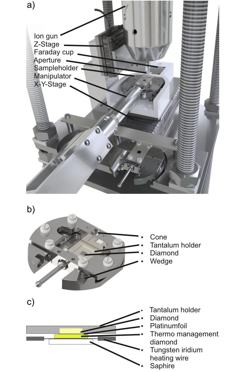 Figure 1
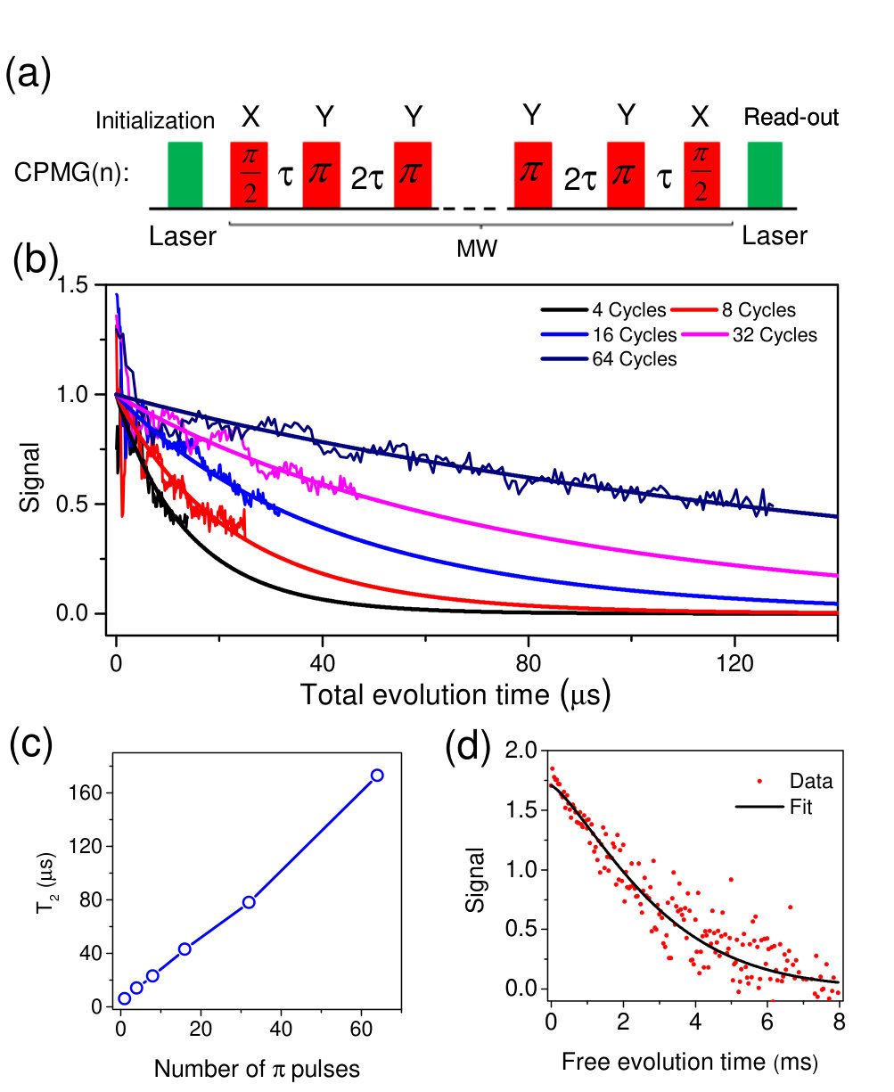 Figure 2
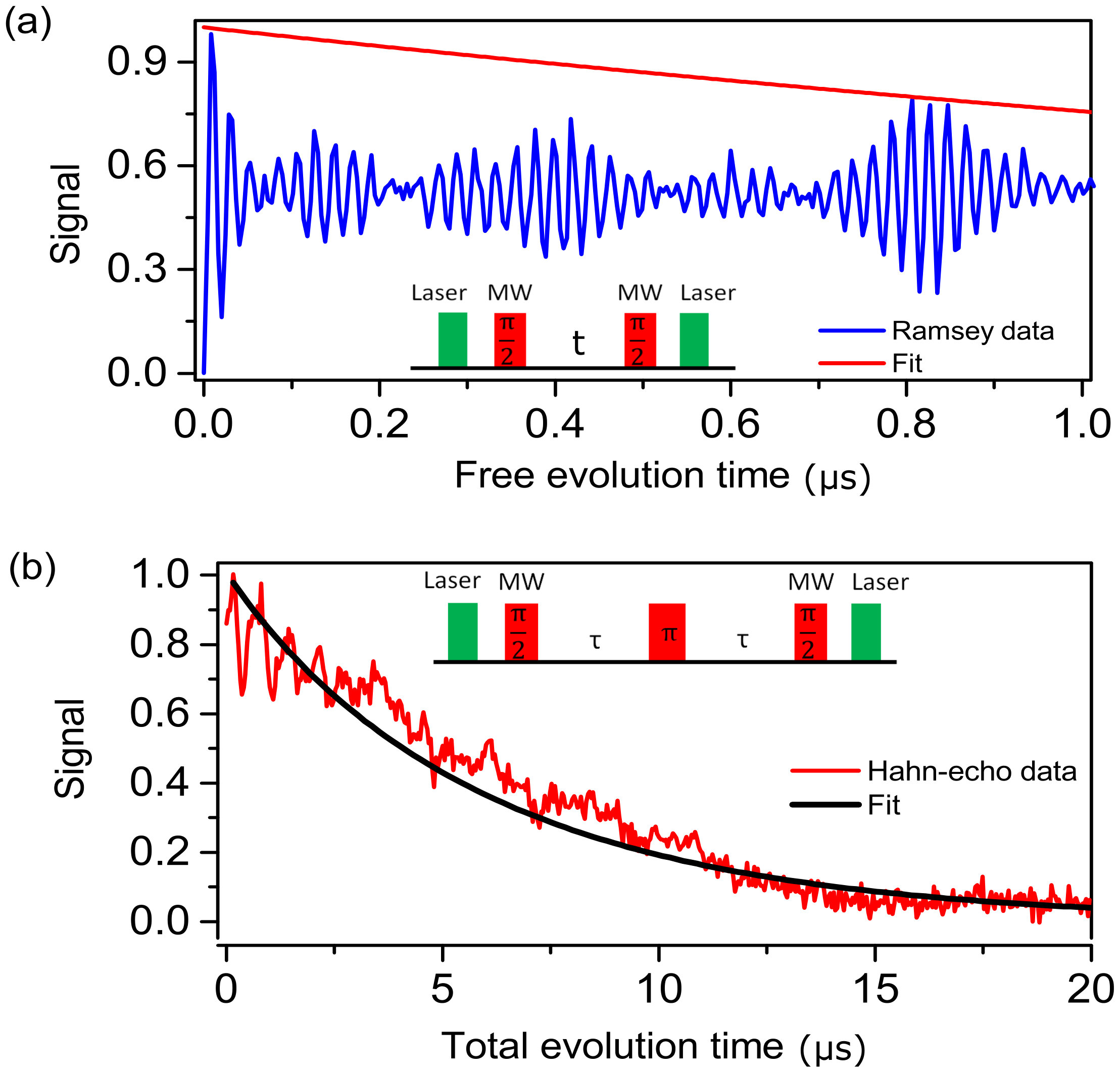 Figure 3
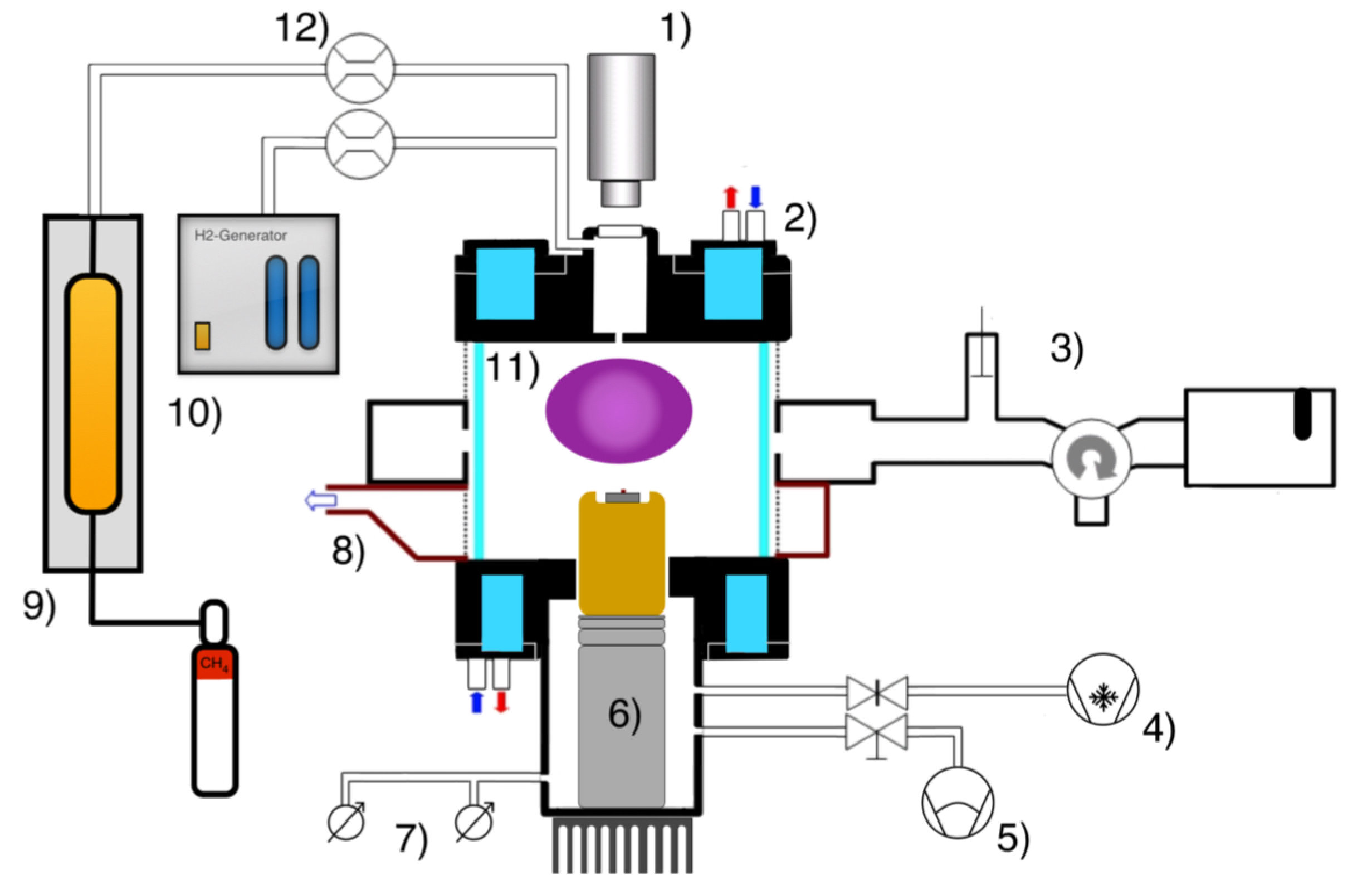 Figure 4
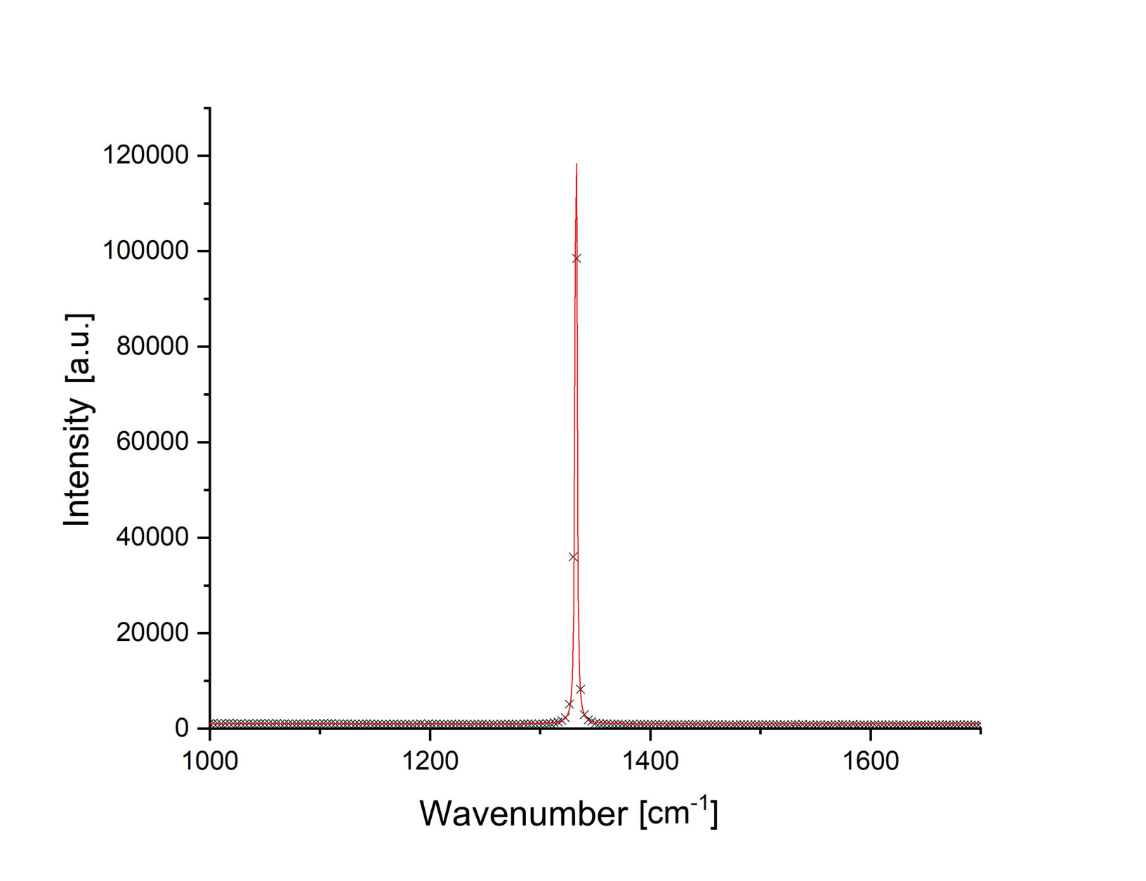 Figure 5
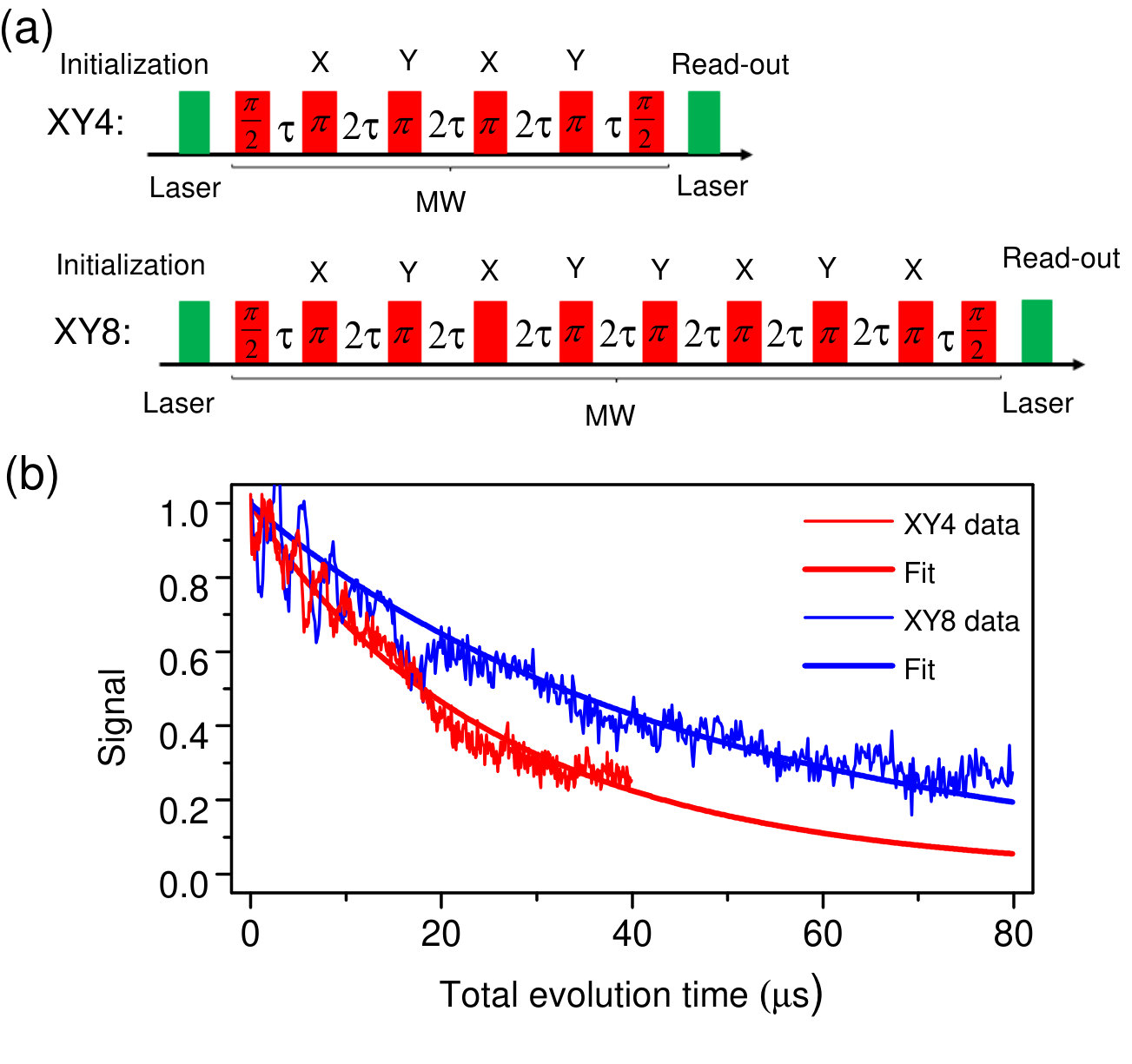 Figure 6
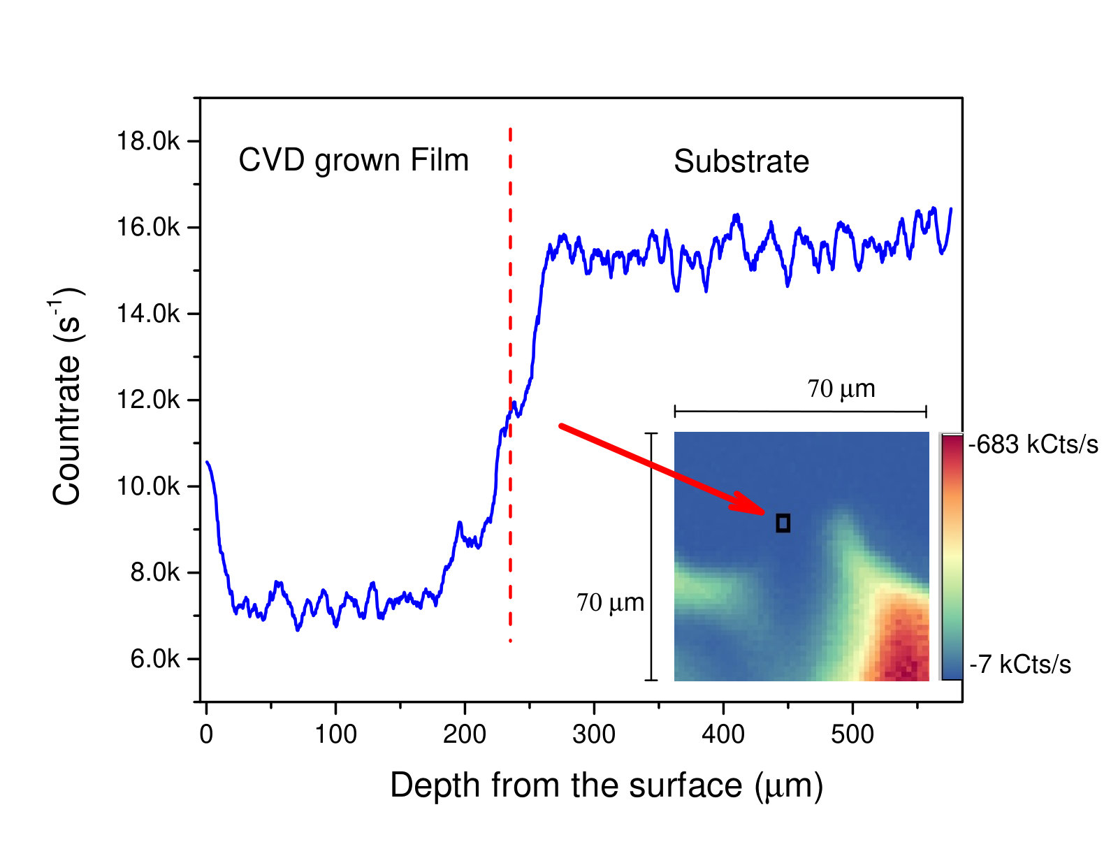 Figure 7
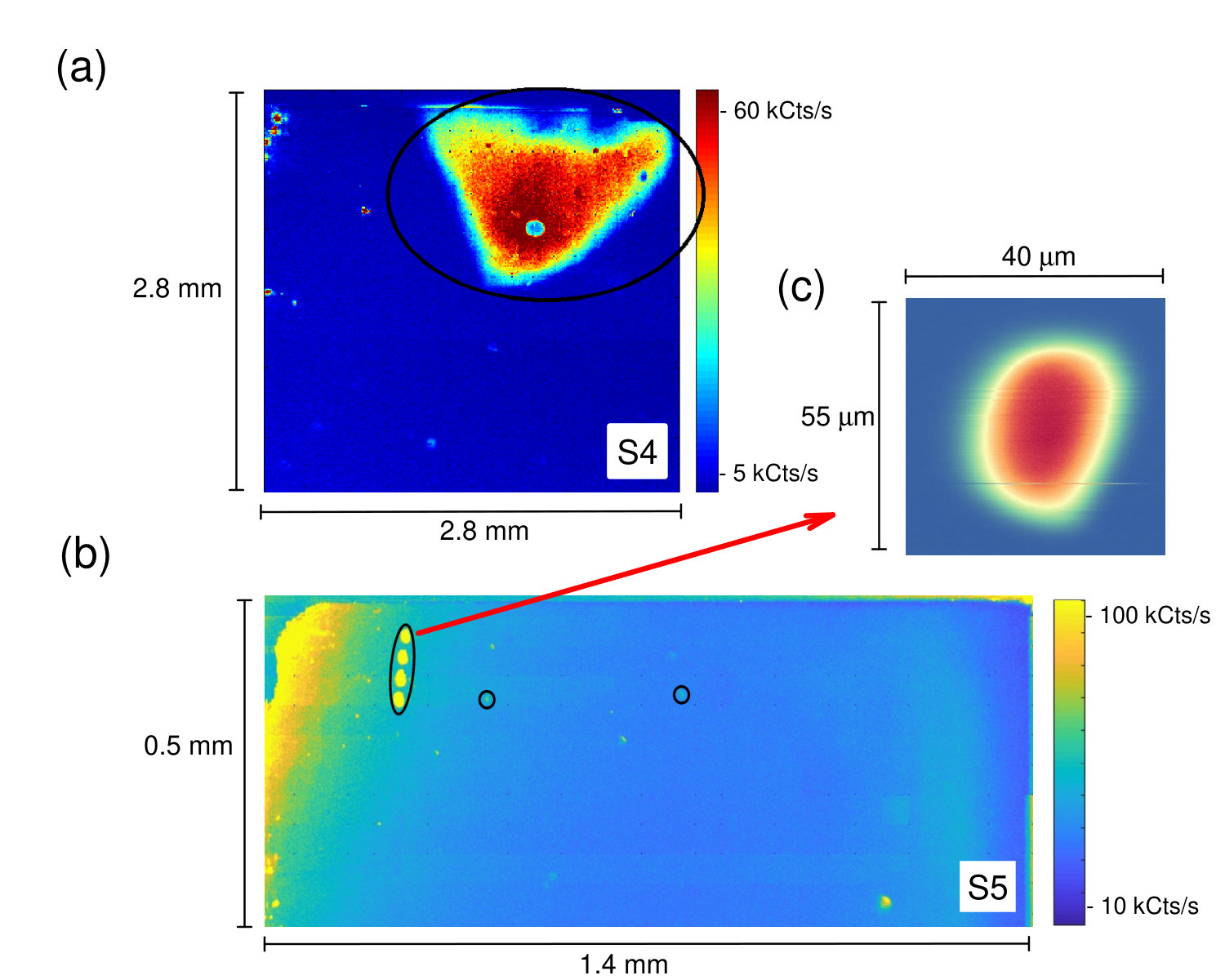 Figure 8
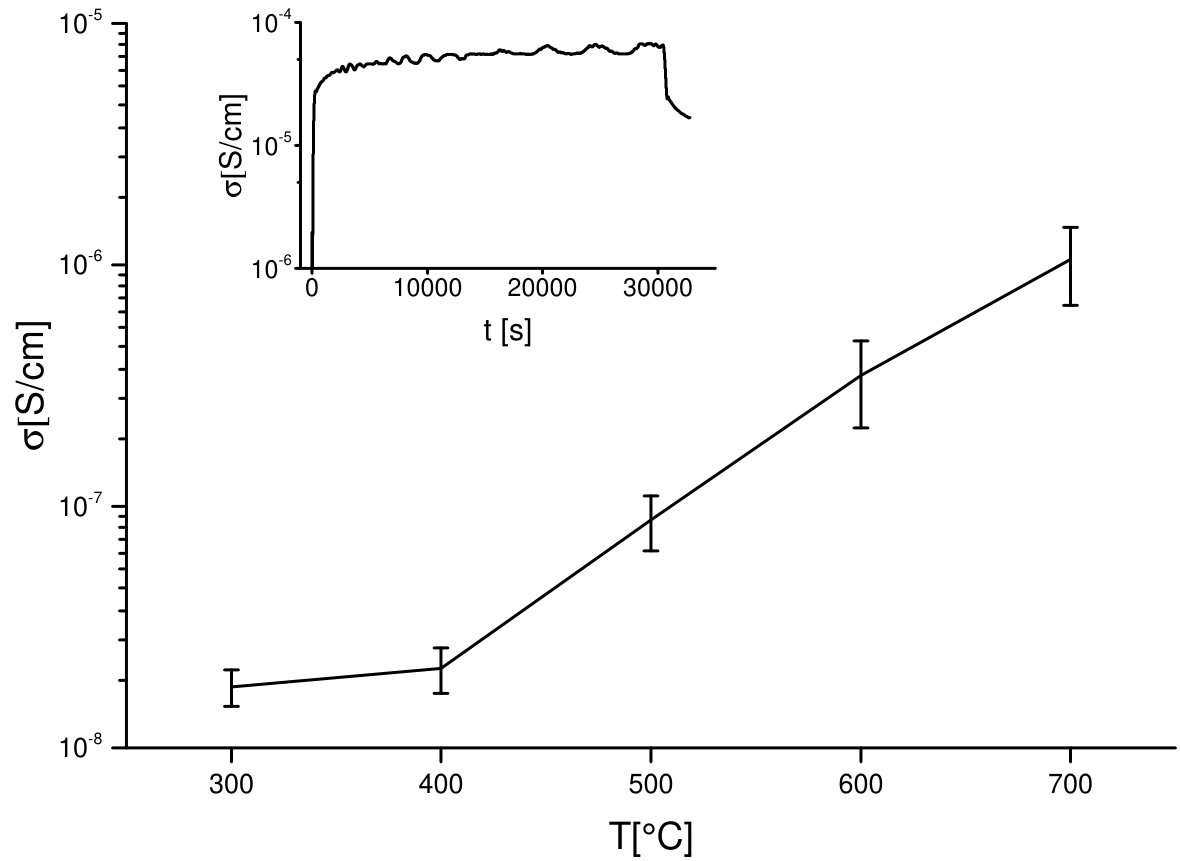 Figure 9
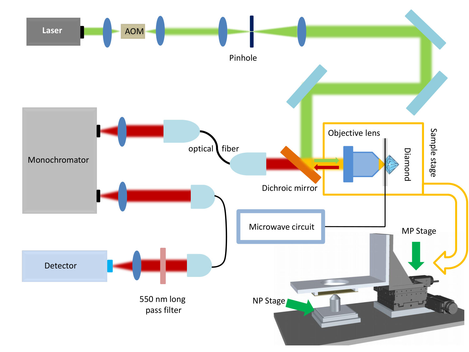 Figure 10
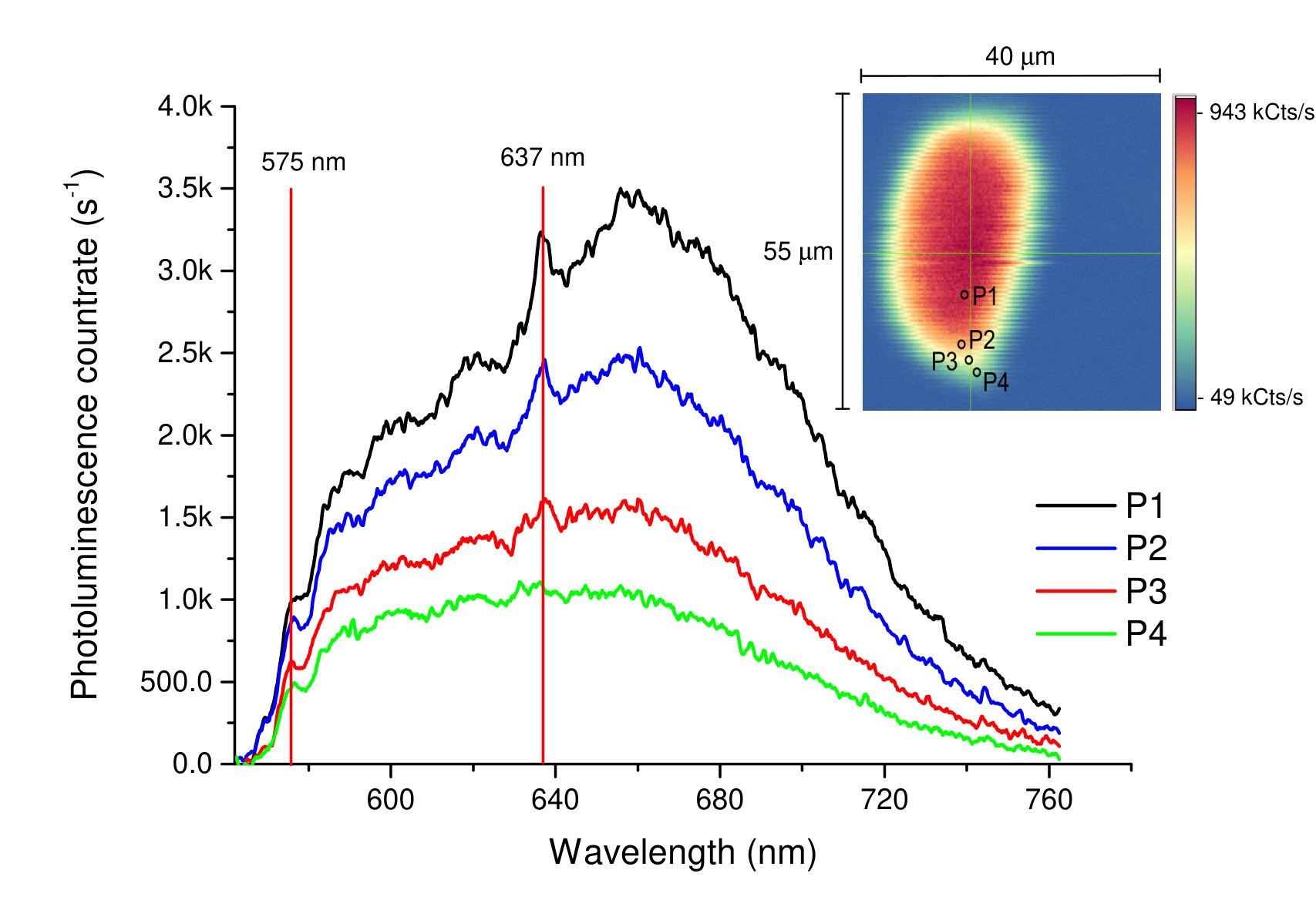 Figure 11
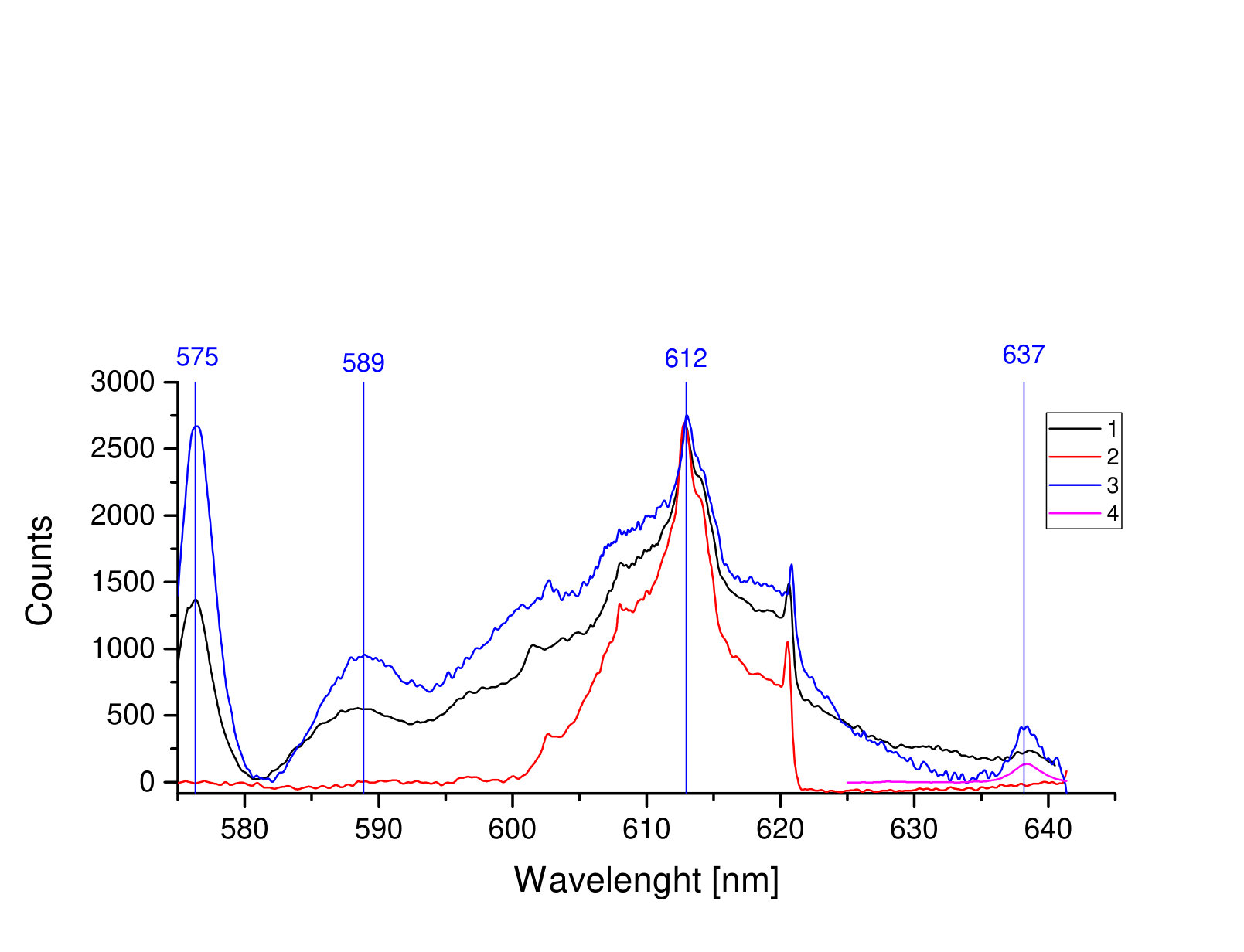 Figure 12
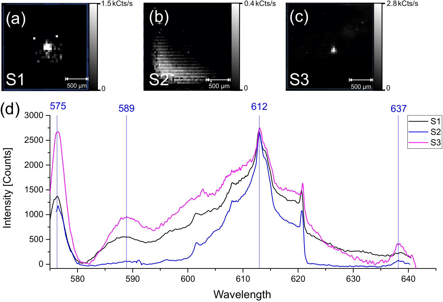 Figure 13
| Parameters | Values |
|---|---|
| Pressure | 170 mbar |
| Gas flow | 400 sccm |
| H2 fraction | 96% |
| CH4fraction | 4% |
| MW-power | 1.6 kW |
| Deposition time | 8 hrs. |
| Substrate | Diamond substrates Ib (001) (electronic grade) |
| Temperature | 9000 C |
| Sample | Precleaning | Termination | Aperture | Dose [cm2] | Implantation temperature [∘C] |
|---|---|---|---|---|---|
| S1 | isopropanol, acetone | Hydrogen | no | 11012 | Room temperature |
| S2 | isopropanol, acetone heated at 800 ∘C | bare | no | 11012 | Room temperature |
| S3 | isopropanol, acetone, heated at 800 ∘C | bare | no | 11012 | 700 |
| S4 | isopropanol, acetone, heated at 800 ∘C | bare | no | 11017 | 700 |
| S5 | isopropanol, acetone, heated at 800 ∘C | bare | yes | 41015 | 700 |
Peer Reviews
No public reviews on file for this paper yet. If you reviewed it on a platform where reviews are public (OpenReview, ICLR, NeurIPS, ICML), you can paste yours below so the community can read it here.
Videos
No videos yet. Explain this paper in a talk, walkthrough, or lecture? Add one.
CVD-growth of ultra-pure diamond, generation of NV centers by ion-implantation
and their spectroscopic characterization for quantum technological applications
T. Chakraborty1,2, F. Lehmann1, J. Zhang1, S. Borgsdorf 3, N. Wöhrl4, R. Remfort4, V. Buck4, U. Köhler3, D. Suter1
1Fakultät Physik, Technische Universität Dortmund, D-44221 Dortmund, Germany
2Institute for Materials Research (IMO), Hasselt University, Wetenschapspark 1, B-3590 Diepenbeek, Belgium
3Experimentalphysik IV, AG Oberflächen, Ruhr-Universität Bochum, Germany
4Faculty of Physics, University Duisburg-Essen and CENIDE, Germany
Abstract
Applications of nitrogen-vacancy (NV) centers in diamond in quantum technology have attracted considerable attention in recent years. Deterministic generation of ensembles of NV centers can advance the research on quantum sensing, many-body quantum systems, multipartite entanglement and so on. Here we report the complete process of controlled generation of NV centers in diamond as well as their characterisation: growing diamond films through chemical vapor deposition (CVD), ion implantation and spectroscopic characterization of the defect centers using a confocal microscope. A microwave-assisted CVD set-up is presented which we constructed for the preparation of single-crystalline homoepitaxial diamond films. The films were prepared with minimized nitrogen concentration, which is confirmed through photoluminescence measurements. We demonstrate an in situ ultra high vacuum (UHV) implantation and heating process for creation of NV centers using a novel experimental set-up. For the first time hot implantation has been shown which prevents surface charging effects. We do not observe graphitization due to UHV heating. By optimizing the implantation parameters it has been possible to implant NV centers in a precise way. We present large area mapping of the samples to determine the distribution of the centers and describe the characterization of the centers by spectroscopic techniques. Reducing the decoherence caused by environmental noise is of primary importance for many applications in quantum technology. We demonstrate improvement on coherence time of the NV spins by suppression of their interaction with the surrounding spin-bath using robust dynamical decoupling sequences.
I Introduction
Quantum technology exploits a handful of solid state systems whose physical properties are determined by quantum effects. The nitrogen-vacancy (NV) color center, a defect center consisting of a substituted nitrogen atom and an adjacent vacancy embedded in a diamond crystal (Jelezko and Wrachtrup, 2006), is one of them. It has several attractive properties, including millisecond-scale spin coherence time, the possibility of manipulating the spins through microwave (MW) pulses, efficient optical initialization and detection of the spins and the ability to perform such experiments at room temperature (Jelezko et al., 2004; Dutt et al., 2007; Chakraborty et al., 2017). These properties make it a useful solid state qubit system which has already been applied in a number of important quantum information experiments like demonstrating long quantum memory by controlling the spin-qubits with high fidelity (Maurer et al., 2012), coherently manipulating individual nuclear spins by specifically addressing a proximal electronic spin (Childress and et al., 2006), exhibiting quantum entanglement between a photon and solid-state spin (Togan et al., 2010), demonstrating quantum interference between two photons (Sipahigil and et al., 2012; Bernien and et al., 2012), implementation of a quantum memory (Fuchs et al., 2011), and quantum repeater (Childress et al., 2006). On the other hand, there has been a significant amount of progress in NV-based sensing technologies where NV centers are applied in imaging the dynamics of neural network (Pham et al., 2011), living cells (Liu et al., 2016; Balasubramanian et al., 2008), probing of superconducting effects (Bouchard et al., 2011), sensing magnetic fields with high precision at the nanoscale (Maze et al., 2008; Taylor et al., 2008; Grinolds et al., 2013) and others. Such promising applications have pioneered a way towards state-of-art NV-based quantum technology.
These sensing applications can be compared to other technological advancements like superconducting quantum interference devices (McDermott et al., 2004), magnetic resonance force microscopy (Rugar et al., 2004), Hall probe microscopy (Chang et al., 1992), optical atomic magnetometer (Xu et al., 2006) have been introduced in the past decades concerning sensing and imaging of magnetic field. Comparison shows that the novel method of magnetic field detection using the NV centers has several advantages over the more conventional techniques. For instance, the NV centers in diamond crystal can be prepared in a controlled fashion: the implantation process can be adjusted to reach a required density of NV centers at a depth of a few nanometers from the surface. This is an essential condition for efficient sensing as such shallow centers can be brought in close proximity (nm) to the magnetic centers under investigation. Importantly, diamond-based sensing can operate at room temperature, in liquid media and normal atmospheric conditions which gives more flexibility and feasibility to such applications. It has been experimentally demonstrated that diamond spins can detect weak magnetic field with high sensitivity and nanometer scale spatial resolution (Maze et al., 2008; Taylor et al., 2008; Balasubramanian et al., 2008).
The sensitivity of NV-based sensors is generally higher if ensembles of centers are used, rather than single centers. Sensing with dense ensembles of NV centers can increase the signal-to-noise ratio as the generated photoluminescence signal increases with , the number of centers being used for detection. Thus, the magnetic sensitivity can be enhanced by a factor when the field is homogeneous over the magnetometer area (Taylor et al., 2008). Furthermore, ensembles of centers are capable of imaging magnetic field over a wide field-of-view range (Hong et al., 2013).
Ensemble of centers has already been applied in different contexts like quantum metrology (Acosta et al., 2009a; Pham et al., 2011), quantum walk (Hardal et al., 2013), device physics (Zhu et al., 2011, 2014; Putz et al., 2014), and quantum simulations (Yang et al., 2012) . In this context, there have been a significant amount of efforts regarding growing highly-pure diamond films and implanting clusters of NV centers with a target pattern suitable for the desired applications.
The primary motivation of this project is to generate ensembles of NV centers in ultra-pure single crystal diamond films in a controlled way with the goal of optimising them for applications in quantum information and sensing technology. The content of the paper has been mainly divided into three parts: the first part deals with growing highly pure single crystalline diamond films. The second part describes the precise creation of near-surface NV centers by ion implantation. In the third part we describe experimental methods for characterizing the centers and we also demonstrate experiments using various dynamical decoupling sequences with an aim to reduce the dephasing of the NV spins due to the environmental noise.
II Homoepitaxial Growth of Diamond
The microwave-activated plasma process (Kamo et al., 1982) has been established as a more efficient technique for the deposition of high-quality single-crystal diamond films than other existing diamond growing techniques like HPHT (high pressure high temperature) crystal growth (Bundy et al., 1955; Liander, 1955) or the hot-filament method (Matsumoto and Setaka, 1981). In this work, pure single-crystal diamond films are homoepitaxially grown by chemical vapor deposition in a microwave assisted CVD plasma source (CYRANNUS® by iplas). We have developed and optimized an experimental set-up for growing diamond films with minimum nitrogen concentration. A schematic diagram of our set up is shown in Fig. 1.The technology of the plasma source CYRANNUS® is based on a cylindrical resonator with annular slots. The microwaves are fed into the ring resonator by a waveguide from which it is coupled into the cylindrical resonator of the reactor. Due to the centric position of the plasma in the reactor, the excitation without electrodes and the short mean free path at the deposition pressure of ca. 200 mbar the interaction of the reactive gas with chamber walls is minimized.
The homoepitaxial growth of diamond by CVD involves the deposition of carbon atoms on a diamond surface that originate from the dissociation of carbon-containing precursors in hydrogen gas. Hydrogen is essential because it selectively etches non-diamond carbon. For the deposition of pure diamond films the hydrogen in this work is generated in a hydrogen generator (HG-1200 by CMC Instruments GmbH) with a purity of 99,99999%. The methane (5.0) is purified (saes Pure Gas Inc.) to gas impurities <1 ppb. Diamond films are grown with a methane and hydrogen mixture with a typical ratio around 4%).
The chamber is evacuated with a scroll pump and a cryopump (CTI-Cryogenics 8200 compressor with cryo-torr pump) and reaches a base pressure of around 10*-9* mbar. Mirror-polished single crystal Ib (001) diamonds (electronic grade) from Element Six Ltd. (< 5 ppb nitrogen impurities) were used as substrates. Substrates were ultrasonically cleaned for 20 min in isopropanol and subsequently 20 min in acetone. During deposition the substrates were kept on a copper substrate holder. Prior to the deposition the substrates were etched in a H2 plasma for 30 min at 170 mbar. After this cleaning step the process parameters were switched to the deposition parameters (Table 1).
The thickness of the grown diamond films and comparison between purity of the substrate and films were determined by measuring PL depth profiles, as described in details in section IV.B.
Raman spectroscopy was performed to determine the crystallinity of the synthesized diamond samples. The data (Figure 2) show a sharp diamond peak at 1332.54 cm*-1* with a FWHM of 1.61 cm*-1* . The narrow line proves the high crystallinity and even exceeds the values for natural and HPHT (high pressure high temperature) single crystals (Shu et al., 2017). The position of the diamond peak indicates that there is almost no intrinsic stress in the grown films. Similar spectra were obtained over the whole surface area.
Secondary Ion Mass Spectroscopy (SIMS) measurements were done to measure the impurities in the deposited diamond films. Since impurities were expected to come from the process gas, we measured the concentration of hydrogen, oxygen and nitrogen in the films. For hydrogen and oxygen the signals were below the detection limits of the instrument. The upper limit of nitrogen concentration was determined using the approach of Gnaser et al. (Gnaser, 2001) as 1.310*-7*(ca. 0.1 ppm). The only other element that was found in the diamond sample in relevant concentrations is silicon. It was measured in PL measurements with a strong ZPL at 738 nm originating from the silicon-vacancy center in diamond. The silicon is supposed to come from the plasma reactor walls since the vacuum chamber consists of a quartz-recipient and the plasma has contact with the wall and etches silicon from the quartz. It was not possible to calculate the concentration of silicon from the PL measurements. Future SIMS measurements will include the determination of the concentration.
The incorporated nitrogen can only come from the process gases or the leakage of the vacuum system. By using a hydrogen generator (cmc Instruments GmbH type HG1200-2T) and pure methane which was additionally purified (Mono Torr type PS4-MT3-531), the purity of the process gases used was 7.0 (99.99999%) for hydrogen and 9.0 (99.9999999%) for CH4, while the leakage of the vacuum chamber was estimated to be around 2.410*-4* sccm. The nitrogen concentration of the grown layer is thus calculated to be below 1 ppb by assuming an incorporation rate of 10*-4*(Jin and Moustakas, 1994).
III Ion Implantation
Two processes are currently used to generate NV centers in diamond. One process is to dose nitrogen in the process gas while growing the CVD diamond. In this process the NV centers are statistically distributed in a well defined plane. It is possible to tune the thickness of this plane (Balasubramanian et al., 2009) and the density of NV centers. The second process is to implant nitrogen with an ion gun into the single crystal diamond (Meijer et al., 2008). For scalable quantum computer architecture and also for magnetometry applications, it is necessary to get control of the accurate positioning of the NV centers in all three axes together with a high probability of creation. It was shown that the yield of creating NV centers can be up to 50% with high implantation energies (2 MeV) (Meijer et al., 2005) but the spatial resolution is very low. The depth and straggling depends on the ion energy and can be calculated with SRIM (Acosta et al., 2009b). It is possible to increase the resolution by implanting with lower energies (1-5 keV) but in this case the yield of creation is reduced to 2.5% (Rabeau et al., 2006). Also, the ion density has an influence on the yield (Pezzagna et al., 2010), therefore it is important to get control of the beam current, the beam profile and the implantation time. To create the NV centers it is necessary to anneal the diamond after the implantation up to 600*∘*
- 800*∘* C for 2 hours which is typically done under high vacuum conditions in a quartz oven after the diamond has been transferred from the implantation chamber. The annealing of the diamond under these conditions often leads to surface graphitization, which must be removed by etching in a boiling triacid (Cui and Hu, 2013).
The diamond surface before and after the implantation is still not well characterized, in particular the influence of the surface on shallow NV centers. To check how treatments influence the quality of the implantation, e.g. lead to a higher background in the confocal signal or harm the coherence time time we want to present a completely new all in ultra high vacuum (UHV) setup where the preparation of the diamond surface, the implantation and annealing process can be done in situ under UHV conditions. Additionally, only in an UHV environment completely non terminated diamond surfaces can be prepared. As received diamonds from Element6 are typically terminated by oxygen because the samplewas cleaned in boiling triacid after the CVD growth. If the diamond is not cleaned in this way, it is hydrogen-terminated after the CVD growth. The influence of oxygen and hydrogen on the ratio NV*-/NV0* has been investigated in detail (Grotz et al., 2012) and it was also found that a hydrogen terminations leads to a surface conductivity on diamond. Our setup gives us for the first time the chance to check systematically the influence of these typical surface terminations on the creation yield for NV centers by comparing them to a non-terminated surface. We use a conventional UHV chamber with a turbo molecular pump, an ion getter pump and a titanium sublimation pump to achieve a base pressure of 510*-11* mbar.
For low-energy nitrogen implantation we use a IQE 12/38 ion source from SPECS. The energy range of the ion gun goes from 400 eV up to 5 keV. The beam diameter (FWHM) is specified to be 150 m. To get a very high purity of nitrogen a Wien-Mass filter is installed, which can also be used to switch between molecular or atomic nitrogen. As a source gas we use 15N2 with a purity of (98 atom %). 15N nitrogen is used to ensure that the NV center was created by implanted nitrogen and not from an abundant one because even with a nitrogen concentration below 5 ppm there would be a chance of 1 native nitrogen atom in a volume of 150 . To measure the beam current a Faraday cup with shielding is installed. The beam diameter was calibrated and measured by scanning the beam over the edge of the Faraday cup. The last parameter which has to be controlled for a correct dose is the implantation time. An electric beam chopper allows to switch on and off the ion beam in 1s and to do 15-1500s pulses. The sample position is controlled by an XY-nanopositioning stage from attoCube with a closed feedback loop. To control the width of the implanted region, a tantalum aperture is used for first test experiments by melting a hole into the tantalum sheet with a diameter of 20 m by a laser beam. The sputter yield for nitrogen on tantalum with 5 keV is very low. So it can be assumed that the contamination of diamond by tantalum is negligible. The aperture is connected to ground to prevent any charging effect and the focus point of the ion beam is set below the sample to achieve a more parallel beam path. The position of the aperture with respect to the sample surface is controlled by a Z-nanopositioning stage. The sample holder (see Fig. 3 b)) was designed to transfer the diamond into the UHV chamber and to the implantation stage below the ion gun (see Fig. 3 a)). The accuracy of placing the sample is below 5m, which was achieved by a cone and wedge placement design. Also it is important to heat the diamond in UHV up to 900*∘C while maintaining a pressure of 110-10* mbar. To achieve this we have designed an effective heating stack (see Fig. 3 c)).
The thermo-management-diamond has a very good thermal conductivity of 2000 W/Km at room temperature. Also at 900*∘C its conductivity is significantly higher than that of sapphire. The platinum foil also collects the thermal radiation of the tungsten iridium heating meander and does not react with the diamond. With this setup we need 12 W electric power to reach 900∘*C on the diamond. Additionally a four point Van-der-Pauw measuring station was installed in the UHV-system to determine the surface conductivity of the diamond after different surface treatments of a pure heated diamond in UHV.
Mapping of the diamond samples was performed with a setup without the XY-Stage and the aperture as it is shown in Fig. 3. To check the influence of different surface treatments on the localization and shape of the implanted area, five implantations were made under different conditions which are discussed below. Table 2 provides an overview of the main sample preparation parameters. Starting from a base pressure of 510*-11* mbar the diffuse N2-pressure during implantation rose to 210*-8* mbar. The dose was 11012 cm2and the beam was focused at the center of the sample. They were heated at 800*∘C for 2 hours under a vacuum of 210-10* mbar after the implantation. Sample 1 (S1) was hydrogen terminated and the implantation was done at room temperature. To check the surface conductivity we use the Van-der-Pauw setup (see inset of Fig. 4). The hydrogen-terminated diamond shows a conductance of 110*-3* S/m at atmospheric conditions and it drops to 310*-4* S/m in UHV which was also reported in (Kubovic et al., 2010). Sample 2 (S2) was cleaned before the implantation by heating the sample up to 800 for 12 hours under a vacuum of 210*-10* mbar. After this treatment the sample was no longer hydrogen or oxygen terminated (Maier et al., 2000),(Maier et al., 2001).Sample 3 (S3) was in the same way cleaned as S2 but the implantation was done at 700*∘C .To check if the heating treatment leads to a higher surface conductivity we measured the surface conductivity for different temperatures of a non terminated diamond with the Van-der-Pauw setup (Fig. 4). It can be seen that the conductance raises up to 110-6* S/m at 700*∘C, which is more than two orders magnitude lower than for S1 but it seems that the electrical conductivity is sufficient to prevent charging during the ion implantation. Optical characterization of the implanted NV centers in S1, S2 and S3 are discussed in section IV(C). In section IV(B) we have demonstrated large area confocal mapping of samples S4 and S5 whose preparation procedures are described below: In the case of S4, the sample was cleaned with isopropanol and acetone, heated in UHV (510-10* mbar) at 7000C for 2 hours, ion implantation without an aperture was performed with an ion dose of 11017cm*-2* and finally heated at 8000C for 2 hours. For sample S5, we implanted four dots in a row with a dose of 11015 cm*-2* and two dots with a dose of 11012 cm*-2* with the same conditions as for S3.
IV Optical Characterisation
For a quantitative characterisation of the samples and to check the success of the implantation, we combine confocal scanning microscopy with optical spectroscopy. To allow scanning of complete samples, with length scales of a few mm with high resolution, we combined a piezoelectrical nanopositioning system (NP) with a motorized micropositioning stage (MP).
IV.1 Setup
Fig. 5 shows a schematic representation of the corresponding setup. A diode-pumped solid-state CW laser, which emits at 532 nm, is used for excitation. An acousto-optical modulator (extinction ratio 57 dB) is used to switch the laser beam on and off. The laser beam subsequently passes through an oil immersion microscope objective (MO) of numerical aperture 1.4, which focuses it into the diamond sample. The PL signal, propagating in the opposite direction of the laser beam, is collected by the same MO and separated from the scattered laser light by the dichroic mirror. The transmitted PL signal is collected into an optical fiber, passes through a 550 nm long pass filter and is measured by a photon-counting detector. Alternatively, it can be sent through a monochromator for spectral analysis. The spot size diameter of our confocal set-up was 0.46 μm. The optical fibers in the detection part provide the flexibility to switch between different types of measurements. The signal from a MW signal generator (APSIN) and an arbitrary waveform generator (AWG) are combined to generate the MW signal for exciting the electron spin transitions of the NV centers. A switch generates MW pulses, which are passed through a 16 W amplifier and a Cu wire attached to the diamond sample.
The confocal microscope combines a nanopositioning (NP) stage with a maximum traveling range of 70 m 70 m in the XY plane and 50 m along the Z-direction with a motorized micropositioning (MP) stage, as shown in the bottom right of Fig. 5. The MO is attached to the NP stage whereas the sample is attached to the MP stage. With this setup, we can scan areas of up to 25 25 mm and generate PL images of XY planes at different depths covering the full diamond samples with nm resolution.
IV.2 Confocal Scanning Microscopy
Fig. 6 (a) and (b) shows the measured full scans of the surfaces for samples S4 and S5 respectively. The important parameters used for preparing S4 and S5 can be found in table 2. The 3 regions marked by ovals in S5 were irradiated with the focused ion beam to generate NV centers; they clearly show the largest fluorescence rates. The parameters for implantation are given in section III. Fig. 6(c) shows that the spot size (m, m) is quite similar to the aperture size of the ion gun. In order to standardize the preparation conditions, instead of preparing the ensembles of centers throughout a diamond substrate, with different implantation parameters like temperature, heating time, ion dose etc., we implanted several NV spots on a single sample and characterized them. This saved both the time and the cost of the diamond substrates. Through these implantations, we also gained better control on precisely creating spots with NVs. Such control is necessary for many quantum technological applications. For example, in case of electrical spin read-out, the NVs should be precisely created in certain positions between the electrodes (Siyushev et al., 2019). Fig. 6(c) shows an enlarged view of one of the four implanted spots marked by the oval as shown by the arrow. From the mapping image shown in Fig. 6(c), we can conclude that the size and position of the implanted area can be controlled in a deterministic way. The PL mapping also indicates that the deposited diamond layer appears to be quite clean. The spectroscopic characterization of this fluorescent spot is described in section IV.3.
The blue area of the sample S4 corresponds to count rates of 5000 s*-1*, which is close to the background rate of our system. In this region, the diamond is very clean, with a very low defect density.
We used similar measurements to characterise the sample along the direction perpendicular to the surface. Since the thickness of the grown films is a few hundred micrometers, we again combined the MP and NP stages to provide sufficient traveling range. We performed spatially resolved PL measurements where the focal position of the MO was varied along the Z-direction through the film. Fig. 7 shows a depth-profile measured at the position indicated in the inset. The data indicates that the film thickness is around 265 m. The recorded count-rate in the grown layer is close to the background rate and is less than the count-rate in the substrate, which indicates that the CVD-grown film has significantly higher purity than the substrate. The relatively thick diamond films of 265 µm were grown to have high purity “bulk-like” diamond films for the implantation of nitrogen. We wanted to ensure that the impurities in the diamond substrate do not affect the investigations of the NV centers on the grown layer. However, the deposition process is very customizable and films can be grown as thin as a few nm as well as up to mm thickness. On the other hand, the distance of the NV centers from the surface is determined by the energy of the nitrogen ions. The energy range of the ion gun goes from 400 eV up to 5 keV resulting in a depth of the NV centers between sub nm scale and 10 nm below the surface of the grown layer. For our samples the depth was between 7 and 10 nm.
IV.3 Optical Spectroscopy
The successful formation of NV centers in the grown diamond films was confirmed by measuring spectra of the the fluorescence emitted by these regions. For each experiment a 22 mm2 map with 5050 pixel2 was done with a Renishaw Raman Spectrometer as a simple spatially resolved spectrometer. At each pixel we recorded a PL-spectrum. Fig. 8 (d) shows some of these spectra. The peaks in the spectra are associated with NV0 ZPL at 575 nm (curves 1 and 3) or NV*-* ZPL at 637 nm (2). An overview of the position and shape of the implanted areas was obtained using the mapping method described above. The details about the samples are mentioned in table 2. The map of sample S1 in Fig. 8(a) shows a spot at the center of the diamond with a diameter of 200 m and a halo of 400 m, which is the spot size that we expected from our experimental condition for implantation: the ion gun was operated with an emission current 100 . Using smaller apertures, we obtained smaller spots, such as the one shown in Fig. 6(c) , which has a diameter of 25 m , obtained with an ion beam current of 500 pA. The spectrum for S1 shows the zero phonon lines (ZPL) of NV0 at 575 nm and of NV*-* at 637 nm, the second order Raman peak between 600 - 620 nm, and a peak at 589 nm that is associated with some point defects possibly created during ion implantation(Zaitsev, 2013). In Fig. 8 (b) S2 shows a strong enlargement of the implantation region on the diamond surface to the lower left corner of the sample. As described in section III, this implantation was performed with a non-terminated and therefore electrically insulating diamond surface. Accordingly, the charges deposited by the beam result in surface charging and subsequent defocussing of the beam. This shows that the bare diamond surface at room temperature is not suited for localized nitrogen implantation at the low energies required for shallow NV centers. The peak for NV*-* has a lower count rate than in the sample S1, which indicates a lower density in the laser stimulated area, caused by the broadening of the beam. The spectrum for S3 shown in Fig. 8 (c) is similar to that of S1 but has slightly stronger features. S3 shows a sharp spot of 150 m diameter without a bright halo. Using the relative ZPL intensities of NV0 and NV*-* charge states for S1, S2 and S3, we estimated their approximate concentration ratios of the measured spots following the method described in ref. (Acosta et al., 2009a). We obtained that equals 0.71, 2.8 and 1.5 for S1, S2 and S3 respectively.
Fig. 9 exhibits a set of 4 spectra measured using the monochromator integrated with the confocal set-up (as described in section IV(A)) at different positions ranging form close to the center of the implanted area towards the periphery, as shown in the inset. The data clearly show the zero phonon lines (ZPL) at 575 nm and 637 nm associated with the NV0 and NV*-* centers respectively, and the corresponding phonon side bands.
V Spin Properties
In this section we describe measurements of the coherence properties of the NV centers by electron spin-dependent fluorescence measurements at room temperature. The negatively charged NV center forms a triplet ground state where the zero field splitting separates the and states by 2.87 GHz (Doherty et al., 2013; Suter and Jelezko, 2017). An external magnetic field lifts the degeneracy of the levels and of the ODMR lines. As an ensemble of NV centers consist of four possible symmetry axes, an applied magnetic field along an arbitrary direction projects itself onto the four axes with four different field values which creates four pairs of electronic transitions and hence eight lines in the ODMR data (Pham, 2013). In our experiments, the orientation of the applied field was along such a direction that the components of the applied magnetic field along the four possible NV axes of the ensemble we measured had similar values, resulting in only 2 lines in the ODMR spectrum. The magnitude of the applied magnetic field was 16 Gauss. By scaling the photoluminescence with respect to the signal from a single center we estimated the concentration of the of the NV centersin the spot which we performed the ODMR measurements as =22 ppm. To measure the coherence properties, we used different experiments that first initialized the system into the bright state () by a 5 laser pulse. From this state, the coherence is generated and manipulated by resonant microwave pulses and the final state is read out by counting fluorescence photons during a second laser pulse whose optimal duration is ns (Suter and Jelezko, 2017).
Fig. 10(a) shows the resulting free-induction decay (FID) signal, measured with a Ramsey-type (Ramsey, 1950) experiment where two pulses separated by a free evolution period were applied between the initialization and read-out laser pulses. The first pulse, with a frequency of 2.8272 GHz, generates a superposition of the spin states and , which subsequently evolves for a time . The second pulse converts one ocmponent of the coherence back into population which is measured during the read-out step. The observed oscillation frequency of 50 MHz is the difference between the carrier frequency of the microwave between the two pulses and the transition frequency. The beats are due to the hyperfine coupling between the electron spin and the 14N nuclear spin. We fitted the envelope of the FID signal to the expression , and calculated =3.6s.
To measure the coherence time , we used the spin-echo sequence introduced by E. L. Hahn (Hahn, 1950). The sequence starts with the 5 initialization laser pulse followed by three MW pulses separated by free precession periods : . The first pulse creates a coherent superposition of the and states and the last one converts the coherence into population difference. The pulse inverts the accumulated phase, resulting in zero overall phase after the second free precession period, provided the environment is static. The experimental data in Fig. 10(b) show the decay of the coherence of the ensemble of NV spins. The envelope of the decay curve is fitted to the expression , where and the exponent depends on the magnetic environment (Bar-Gill et al., 2012; Pham et al., 2012). We obtained (Hahn echo)= and .
Preserving the coherence of quantum states on a longer timescale is essential for quantum information and sensing protocols (Ladd et al., 2010; Maurer et al., 2012; Putz et al., 2014). Decoherence of the spins belonging to NV centers happens due to their undesired interaction with the magnetic environment mainly caused by the electronic spins of substitutional nitrogen centers and nuclear spins (De Lange et al., 2010, 2011; Naydenov et al., 2011; Ryan et al., 2010). To protect quantum states from decoherence, dynamical decoupling (DD) has been established as an efficient technique (Souza et al., 2012; Suter and Álvarez, 2016). It decouples the system spins from the surrounding spin-bath by applying a periodic sequence of inversion pulses that effectively isolate the system spin from the environmental noise (De Lange et al., 2010; Bar-Gill et al., 2013; Pham et al., 2012; Naydenov et al., 2011; Bar-Gill et al., 2012).
Here, we demonstrate that the electronic spins in our samples respond well to the dynamical decoupling sequences and we are able to extend the coherence time beyond the values obtained in the Hahn-echo measurements described above. For this purpose, we use the Carr–Purcell–Meiboom–Gill (CPMG) pulse sequence, a robust DD technique which has been extensively used in NMR spectroscopy (Souza et al., 2012). The CPMG sequence can be considered as an extended version of the Hahn-echo sequence where multiple refocusing pulses are applied during the free evolution period between the two pulses, as shown in Fig. 11(a). We implemented CPMG sequences with the number of control pulses varying from 4 to 64. The measured decoherence curves as a function of total free evolution time and their fit to the expression are plotted in Fig. 11(b). We have determined the coherence time for the ensemble of NV spins from the above analysis and observed its extension by almost 29 times for 64 pulses [] over the corresponding value measured by the Hahn-echo. The variation of with is shown in Fig. 11(c). We also measured the spin-lattice relaxation time for the same ensemble of NV centers. Fig. 11(d) shows the measured data along with the theoretical fit to the expression . We obtained ms and =1.32. For short echo times, a part of the signal decays more rapidly. This appears to be due to some initial transients that precess around the effective field but die out after a few microseconds.
While the CPMG sequence is well suited for preserving a given quantum state, it is rather unsuited for protecting unknown quantum states (Maudsley, 1986; Souza et al., 2011). For such cases, it is therefore important to use a pulse sequence that performs well for arbitrary initial conditions. We therefore repeated the measurement with the pulse sequences XY4 and XY8. They are well established as robust and symmetrized sequences (Maudsley, 1986; Souza et al., 2011; De Lange et al., 2011; Ryan et al., 2010). They consist of a series of pulses around two perpendicular rotation axes as shown in Fig. 12(a). The experimental decay curves obtained with the XY4 and XY8 sequences are shown in Fig. 12(b) together with the corresponding fits. We were able to extend up to and by using the XY4 and XY8 sequences, respectively.
The sensitivity of a spin based magnetometer is limited by the photon shot-noise when the readout is performed optically. An effective way to enhance the shot-noise limited sensitivity is to use a large number of NV spins which can enhance the collected PL signal significantly. Moreover, reduced dephasing and an enhancement in the coherence time of the NV spins can directly improve the sensitivity. Here, we try to overcome these issues by creating ensembles of NV centers with superior coherence properties and examine the sensitivity of our possible NV based magnetometer. Thus, following the speculation of ref. (Taylor et al., 2008), we can conclude that in ideal measurement conditions for an NV-based magnetometer exploiting the NV centers we prepared, an NV concentration ppm and coherence time can give a DC magnetic field sensitivity up to 100 nT Hz*-1/2* . On the other hand, by appying the DD sequences we could enhance the coherence time (DD) significantly which can increase the sensitivity to ac magnetic field by a factor of For instance, using the DD sequence CPMG(64) we can obtain 10 nT Hz*-1/2* .
VI Conclusion
Through this project we have described the deterministic preparation of ensembles of NV centers in ultra-pure diamond films through three major steps: growing the diamond films, implanting the NV centers and characterizing them. A plasma assisted CVD reactor for depositing high purity diamond films was constructed and optimized to minimize the nitrogen content in the synthesized films. High-purity films with a thickness of 260 μm at a growth rate of about 30 μm/h with constant high crystal quality were deposited. The nitrogen content of the deposited diamond layers is below the detection limits of the standard methods of analytical chemistry or physics. The upper limit for nitrogen in our films was measured to be 1.310*-7*(ca. 0.1 ppm) which refers that our films are at least among the purest diamonds substrates that are commercially available. In the future we plan to perform measurements like EPR to see whether these samples are having even better purity than the commercial available ones.
A novel experimental set-up for in situ preparation of the diamond surface, implantation and high temperature annealing has been presented. In conclusion it was observed that it is possible with this new method to create NV centers while heating the diamond in UHV without strong defocussing effects. It was shown that it is possible to create localized NV centers on hydrogen terminated and heated diamonds. Optimized implantation parameters have been obtained which enabled us to precisely implant NV centers. Using the above described implantation through an aperture, we could implant spots with sizes similar to the aperture of the ion gun in a deterministic way, thus achieving better a better localization of the NV centers. The experimental protocol of large area scanning has been demonstrated which enables us to record the PL image of the full sample in mm scale with nm resolution. Optical spectroscopic measurements have ascertained the generation of NV centers. Next, we have demonstrated the potentiality for possible application of the created NV centers in quantum information and sensing by preserving the coherence for extended times. We observed that the NV spins respond well to different robust dynamical decoupling sequences. The coherence time has been extended and dephasing of he spins has been delayed in a controlled fashion. We can conclude that a magnetic sensor designed using the sample we prepared can reach a sensitivity of 10 nT Hz*-1/2* under optimized experimental conditions.
In the future we plan to improve the coherence properties of the spins by creating NV centers in isotopically purified 12C enriched diamond with 13C concentration below and improve the sensitivity to ac and dc magnetic field. Moreover, we plan to design an ion gun with nm aperture and install a single ion counter which will allow us to optimize the implantation dose and hence, the NV concentration. These experimental upgrades will allow us to deterministically implant ordered arrays of single NV centers which can function as an efficient large-scale solid-state quantum register.
Acknowledgements.
We acknowledge K. R. K. Rao for his assistance with developing the software for area scanning experiments. The research under this project was supported by the funding from Mercator Research Center Ruhr (MERCUR).
The reference list from the paper itself. Each links out to its DOI / PubMed record.
- 1Jelezko and Wrachtrup (2006) F. Jelezko and J. Wrachtrup, Phys. Stat. Sol. (a) 13 , 3207 (2006).
- 2Jelezko et al. (2004) F. Jelezko, T. Gaebel, I. Popa, M. Domhan, A. Gruber, and J. Wrachtrup, Phys. Rev. Lett. 93 , 130501 (2004).
- 3Dutt et al. (2007) M. V. G. Dutt, L. Childress, L. Jiang, E. Togan, J. Maze, F. Jelezko, A. S. Zibrov, P. R. Hemmer, and M. D. Lukin, Phys. Rev. Lett. 316 , 1312 (2007).
- 4Chakraborty et al. (2017) T. Chakraborty, J. Zhang, and D. Suter, New J. Phys. 19 , 073030 (2017).
- 5Maurer et al. (2012) P. C. Maurer, G. Kucsko, C. Latta, L. Jiang, N. Y. Yao, S. D. Bennett, F. Pastawski, D. Hunger, N. Chisholm, M. Markham, D. J. Twitchen, J. I. Cirac, and M. D. Lukin, Science 336 , 1283 (2012).
- 6Childress and et al. (2006) L. Childress and et al., Science 314 , 281 (2006).
- 7Togan et al. (2010) E. Togan, Y. Chu, A. S. Trifonov, L. Jiang, J. Maze, L. Childress, M. V. G. Dutt, A. S. SÞrensen, P. R. Hemmer, A. S. Zibrov, and M. D. Lukin, Nature 466 , 730 (2010).
- 8Sipahigil and et al. (2012) A. Sipahigil and et al., Phys. Rev. Lett. 108 , 143601 (2012).