Synaptic dynamics in complex self-assembled nanoparticle networks
S. K. Bose, S. Shirai, J. B. Mallinson, and S. A. Brown

TL;DR
This study investigates neuromorphic switching in complex nanoparticle networks, demonstrating controllable synapse-like behavior influenced by electric stimuli, network morphology, and inter-synapse interactions, with implications for neuromorphic computing.
Contribution
It provides a detailed analysis of switching dynamics in self-assembled nanoparticle networks, highlighting how electric stimuli and network structure influence neuromorphic behavior.
Findings
Switching occurs above a voltage threshold with rates increasing at higher voltages.
Two distinct behavioral archetypes of switching are identified.
Network morphology and conductance constrain device properties.
Abstract
We report a detailed study of neuromorphic switching behaviour in inherently complex percolating networks of self-assembled metal nanoparticles. We show that variation of the strength and duration of the electric field applied to this network of synapse-like atomic switches allows us to control the switching dynamics. Switching is observed for voltages above a well-defined threshold, with higher voltages leading to increased switching rates. We demonstrate two behavioral archetypes and show how the switching dynamics change as a function of duration and amplitude of the voltage stimulus. We show that the state of each synapse can influence the activity of the other synapses, leading to complex switching dynamics. We further demonstrate the influence of the morphology of the network on the measured device properties, and the constraints imposed by the overall network conductance. The…
Click any figure to enlarge with its caption.
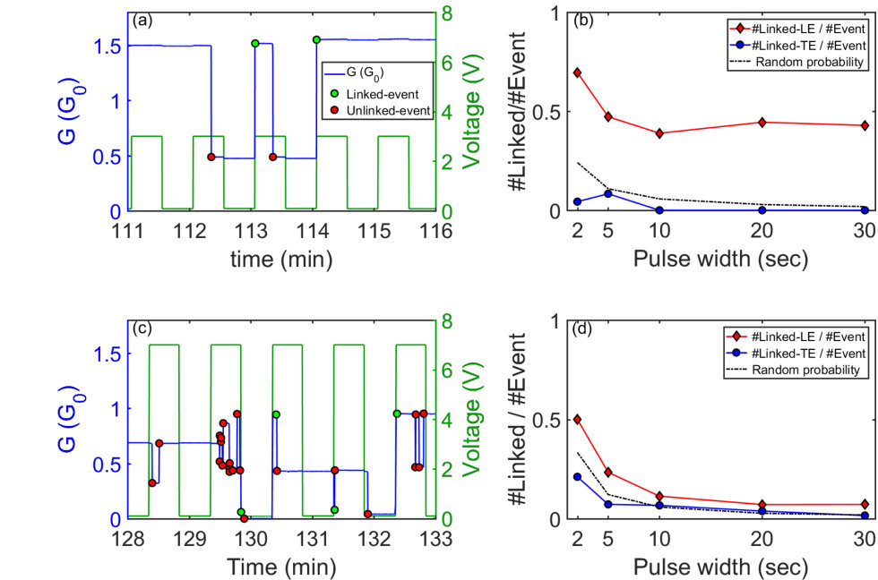 Figure 1
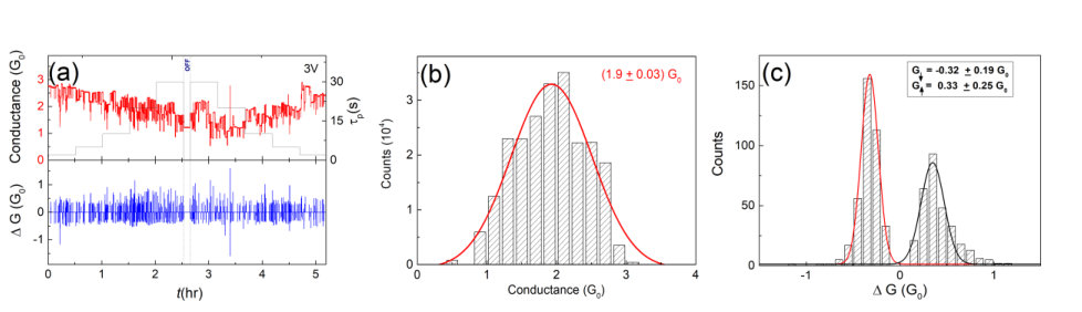 Figure 2
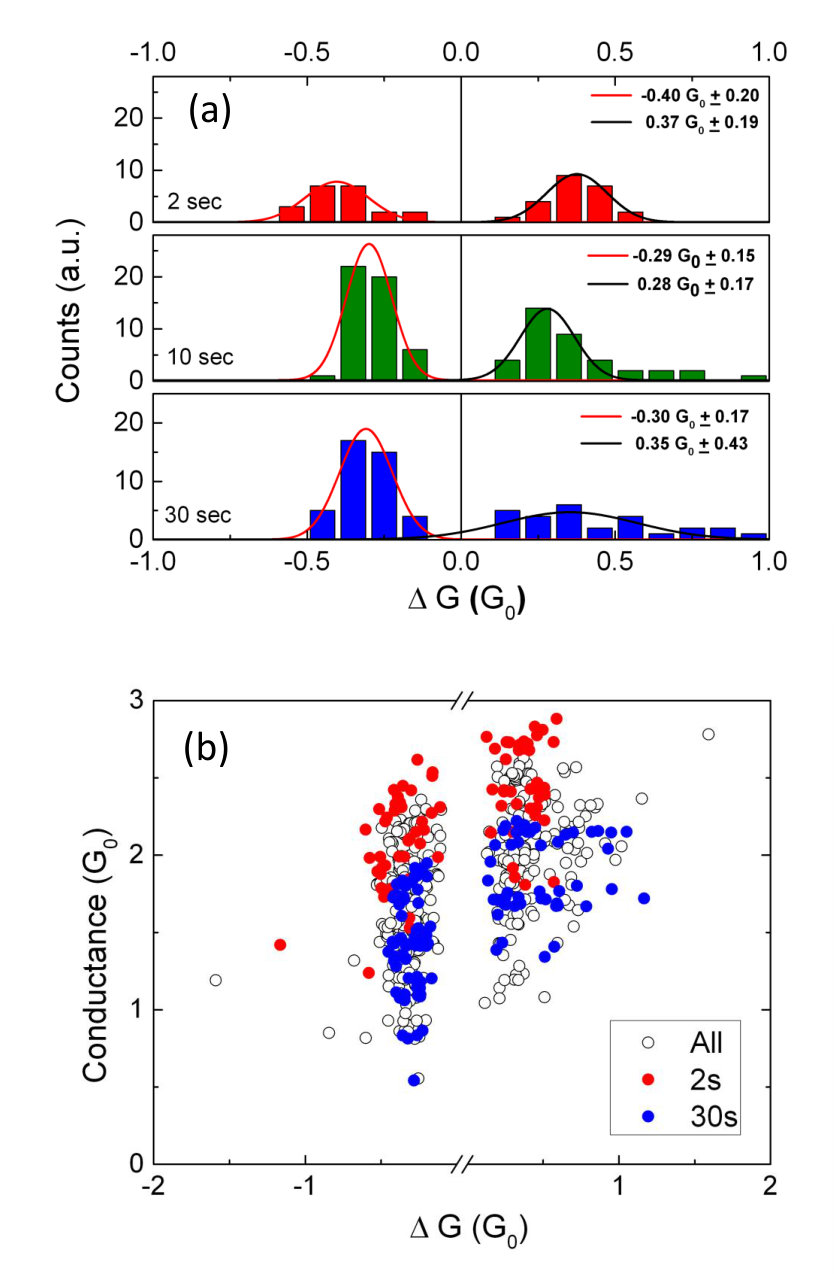 Figure 3
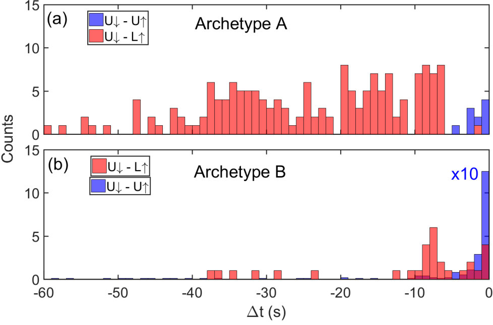 Figure 4
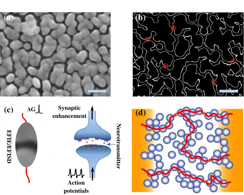 Figure 5
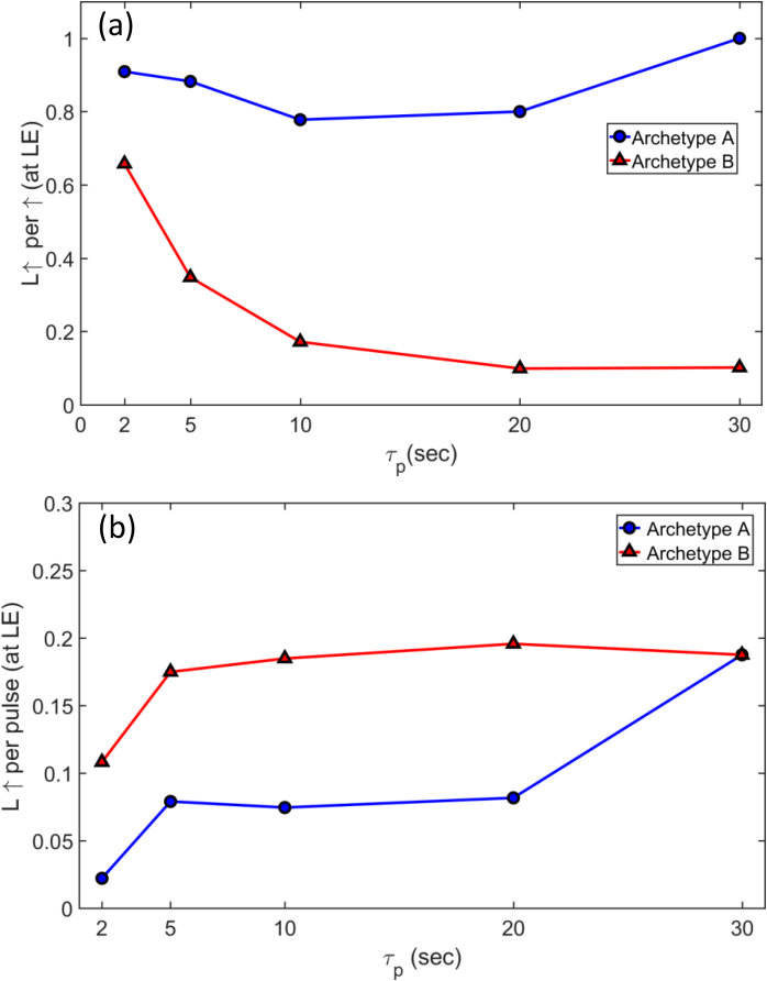 Figure 6
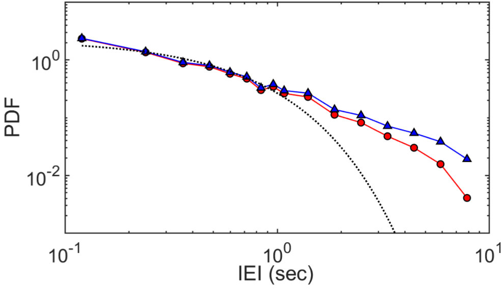 Figure 7
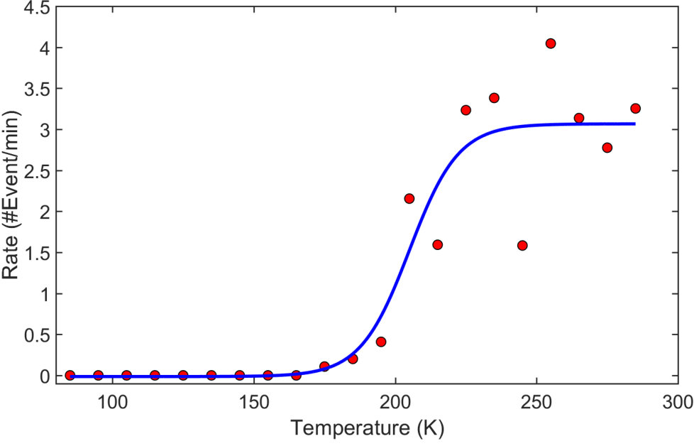 Figure 8
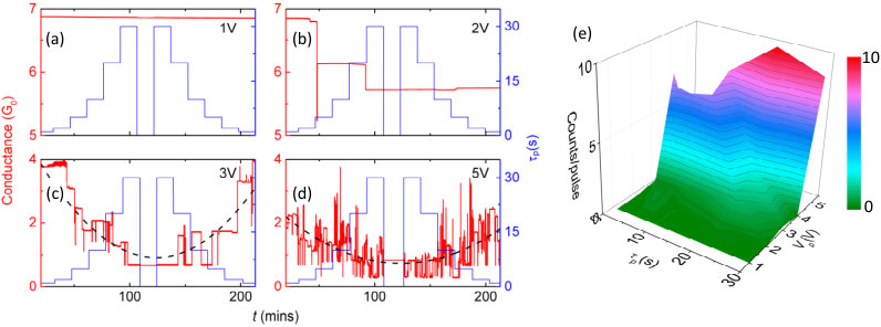 Figure 9
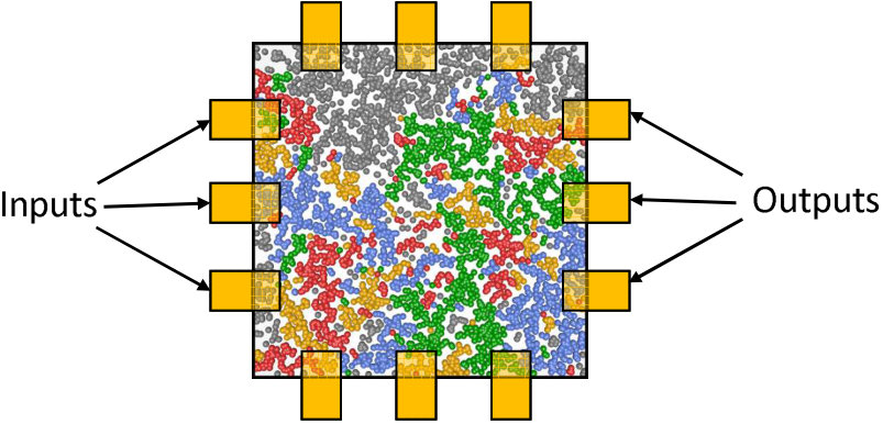 Figure 10
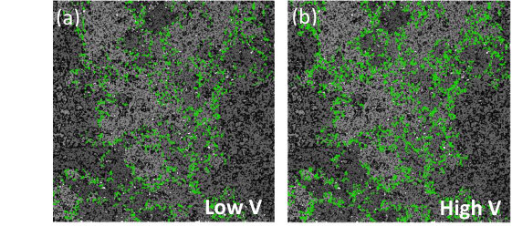 Figure 11
Peer Reviews
No public reviews on file for this paper yet. If you reviewed it on a platform where reviews are public (OpenReview, ICLR, NeurIPS, ICML), you can paste yours below so the community can read it here.
Videos
No videos yet. Explain this paper in a talk, walkthrough, or lecture? Add one.
Synaptic dynamics in complex self-assembled nanoparticle networks
S. K. Bose,a S. Shirai,a J. B. Mallinson,a and S. A. Browna
Abstract
We report a detailed study of neuromorphic switching behaviour in inherently complex percolating networks of self-assembled metal nanoparticles. We show that variation of the strength and duration of the electric field applied to this network of synapse-like atomic switches allows us to control the switching dynamics. Switching is observed for voltages above a well-defined threshold, with higher voltages leading to increased switching rates. We demonstrate two behavioral archetypes and show how the switching dynamics change as a function of duration and amplitude of the voltage stimulus. We show that the state of each synapse can influence the activity of the other synapses, leading to complex switching dynamics. We further demonstrate the influence of the morphology of the network on the measured device properties, and the constraints imposed by the overall network conductance. The correlated switching dynamics, device stability over long periods, and the simplicity of the device fabrication provide an attractive pathway to practical implementation of on-chip neuromorphic computing.
00footnotetext: a* The MacDiarmid Institute for Advanced Materials and Nanotechnology, School of Physical and Chemical Sciences, University of Canterbury, Private Bag 4800, Christchurch 8140, New Zealand. E-mail: [email protected]; [email protected]*
.
This is a post-peer-review, pre-copyedit version of an article published in Faraday Discussions. The final authenticated version is available online at: http://dx.doi.org/10.1039/c8fd00109j
1 Introduction
The quest to replicate the most advanced computer, i.e. the biological brain, has led to immense advancements in software and hardware emulation of the organic neuronal and synaptic structures.1, 2, 3 The central concepts are that nanoscale switching elements, whose state (resistance) reflects the history of their inputs (hence the name ‘memristors’)4 can be used to emulate the functions of biological synapses, and that networks of such elements could potentially replicate some of the functions of the brain.5, 6, 7, 8, 9, 10, 11 Recent work has shown that memristor networks can potentially be used for many tasks, ranging from simple pattern recognition and associative learning 12, 13 to more complex applications requiring greater functionality.7, 6, 11, 8
A wide variety of types of memristive element 14, 15, 16 and types of network 9, 10, 11 have been proposed, each of which has strengths and weaknesses. Highly organised arrays of memristors7, 17, 18 can take advantage of established lithography techniques, but suffer from the same cost and fabrication limitations as traditional complementary metal-oxide-semiconductor (CMOS) devices.19, 20 Self-organised networks10, 21 might provide similar functionality using low-cost fabrication techniques as well as genuinely neuromorphic structures that have the built-in complexity that is believed to be important for brain-like functionality.22, 23
Here we focus on networks of metallic nanoparticles which, when poised near the percolation threshold, exhibit complex switching behaviour due to the formation and annihilation of atomic scale wires within tunnel gaps in the network24. Switching events that cause increases (decreases) in device conductance () are understood24, 25 to be due to electric-field-induced formation26 (electromigration-induced annihilation27) of atomic-wires in tunnel gaps within the network. These atomic-switches act as inorganic-synapses and multiple such switching events (synaptic reconfigurations) in different locations lead to complex switching dynamics. It has recently been shown that these synaptic networks can be fabricated such that devices work reproducibly for several months.28
Since the networks are complex, it is intrinsically difficult to separate out the switching of the individual elements from the observed changes of the network as a whole. Here we apply controlled voltage pulses and characterize the resultant network dynamics. We show that there is a well-defined threshold voltage () for the onset of switching, and that the atomic wire formation processes occur effectively instantaneously on the timescale of our existing measurement system. Synaptic reconfiguration with voltage stimulus close to , where wire breaking processes occur on longer time scales and individual switching events can be resolved, simplifies the data analysis. The formation and annihilation of atomic-wires in individual synapses appear to be temporally stochastic, which is believed to be advantageous for some neuromorphic computation paradigms16, 29. Each synapse is inter-connected with the complex network and we show here preliminary evidence suggesting heavy tailed distributions of inter-event-intervals (times between switching events), which are characteristic of correlations.30, 9 We also show that the morphology of the network controls its resistance and therefore shifts the measured conductance away from the quantised conductance values expected for individual atomic scale wires.31, 24 Finally we outline the prospects for further device and applications development.
2 Experimental
Our devices are fabricated using simple cluster deposition techniques that have been described in detail previously 32, 28. Briefly, tin clusters ( 8.5 nm) are deposited between Au contacts (100 m separation) in a controlled atmosphere containing a small amount of air ( Torr) with high relative humidity,28 resulting in the morphology shown in Fig. 1 (a). Deposition is terminated when the device resistance reaches 2k (, where is the quantum of conduction33, 34).
3 Results I: Network dynamics
3.1 Synaptic network of atomic-switches
Near the percolation threshold, networks of self-assembled nanoparticles contain a multitude of interconnected atomic-switches.24, 28, 21 Fig. 1 (a) shows a typical scanning electron micrograph (SEM) of such a network with percolating pathways. The corresponding edge marking in Fig. 1 (b) reveals the presence of gaps in these pathways, some of which are indicated by red-circles. These are potential zones for atomic-wire formation (and annihilation) which can be modelled14 as inorganic counterparts of the organic synapses in the biological brain. The arrival of an appropriate action potential on a biological synapse has a finite probability of enhancing the synaptic connection in Fig. 1(c). In our inorganic-synapse (atomic-switch), the voltage-pulse stimulus can initiate electric-field induced atomic-rearrangements leading to formation of an atomic-wire bridging the gap, and thus enhancing the overall device conductance. Continuous current flow through these wires can reset the synapse via electromigration. The effect of individual synaptic reconfigurations on the measured device conductance i.e. () is dependent upon the spatial as well as temporal configuration, i.e. the position of the synapse in the network. A very simplistic depiction of such a network is shown in Fig. 1 (d). This complex synaptic network could be imagined as a dynamic reservoir35, 36, 12 of interconnected and interdependent synaptic ‘weights’. Reservoir computing (RC) using such atomic switch networks is believed to be a powerful tool for a range of problems including pattern recognition10, 35, 28, 37 and various waveform regression tasks 38.
3.2 Network activity and event-rates
Excitation of the complex network with voltage pulses initiates synaptic reconfigurations as shown in Fig. 2. The variation of conductance of a typical device in response to our standard pulse sequence (pulse widths from 2s to 30s and back to 2s) and when the pulse amplitude is increased is shown in Figs. 2(a) to (d). The 1V and 2V pulses result in few switching events, whereas voltages above 3V lead to a characteristic dependence on pulse width (parabolae are guides to the eye) in which the long pulses result in a lower average . There are absolutely no switching events for read voltages [ 100mV, centre regions in Fig. 2(a-d)]: this stability for sub-threshold voltages () has been verified for extended periods (weeks) of time.28 Every time a synapse connects/disconnects the electric field and current distribution is rearranged and subsequent synaptic activity is dependent upon the modified network state. As is increased beyond switching becomes more active and the devices reach a state in which the average conductance is . Active switching around this conductance value can be observed for many months.28 Fig. 2(e) summarizes the dependence of the number of events/pulse as a function of and , and emphasises the dramatic increase in activity of the network for stronger excitation pulses (higher ).
This enhanced device activity (higher rate of events) could be due to either increased activity of the same synapses or activation of new previously inactive synapses. To better understand this, results from numerical simulations21 are shown in Fig. 3. Similar to experimental measurements, the voltage stimulus is applied on the left side of the network with right side being grounded. Various groups of ohmically connected particles are connected via the active synapses indicated by green markers (i.e. atomic-switches that reconfigured). As can be seen in Fig. 3(b) the overall density of the active synapses increases at higher voltage which suggests that the experimental observation of increased event-rates at higher voltages can be attributed, at least partially, to the activation of additional synapses. This can be understood intuitively as being due to the increased electric field in tunnel junctions in which the field was previously below a minimum value required to cause atomic motion. In the next section we explore the synaptic dynamics using temperature dependent measurements.
3.2.1 Temperature dependence of event rates
The synaptic activity can be arrested by decreasing the device temperature (T). As shown in Fig. 4 lowering the temperature below 200K, results in no switching events being observed even when 8V pulses are applied. Application of different voltage pulse amplitudes and pulse-widths (not shown here) leads to similar results. This demonstrates that the typical energy scale necessary for atomic-reconfiguration is 17 meV. This energy scale is very similar to the Debye temperature of Sn39. Below 200K the atomic motion is ‘frozen out’, effectively preventing diffusion of adatoms in the tunnel gaps and eliminating the atomic-wire formation processes.
3.3 Threshold switching: archetype-A
We now explore the switching dynamics in the near threshold regime (V Vth) where the number of synaptic events is minimized and thus the switching behaviour simplifies. Any voltage pulse stimulus consists of four components i.e. a leading-edge (LE) where voltage increases from off (read voltage 0.1V) to on, trailing-edge (TE) when V decreases from on to off, and on and off regions. Fig. 5(a) presents a typical snapshot example of a G(t) trace with close to but above . The green markers label events at the pulse-edges as “linked-events" and the red markers denote events in the on region as “unlinked-events". As can be seen in Fig. 5(a) for V Vth the events occur almost exclusively at the leading edges of the pulses, showing that the electric-field-induced formation of atomic scale wires occurs on a timescale that is effectively instantaneous111Ref. 40 shows that switching can take place on timescales of nanoseconds.. In contrast, all events are unlinked, and occur after several seconds of current flow, consistent with the idea that electromigration breaks the atomic scale wires to reset the synapse. We identify this behavior as archetype-A.
Analysis of the switching events over many measurement cycles shows the events are predominantly observed at the leading-edge (LE) of the pulse [Fig. 5(b)]. The fraction of events that are linked at the LE (red-diamonds), as a function of the pulse width p, is much higher than possible from a random distribution of events (dotted-line). This indicates that a certain proportion of the tunnel gaps in the network respond instantaneously to the applied electric field. In contrast the number of linked-events at the TE is consistent with random occurrence, i.e. these events occur at the TE simply by chance, they are not driven by the changing electric field.
3.4 V > Vth: archetype-B
At higher voltages i.e. V the archetype-A behavior evolves into more complex archetype-B behavior. Fig. 5(c) depicts a typical G(t) snapshot and shows that, in addition to the linked-up events at LE, additional unlinked events (U and U) occur. This behaviour is consistent for all and across devices. Similar to archetype-A, the linked-events occur at the LE, rather than the TE.
Fig. 6(a) shows the variation of the number of linked-up (L) events at the LE as a fraction of the total events (). For archetype-A, L is nearly 1 i.e. 100%, with a negligible fraction of U for all . In contrast, in archetype-B, the ratio L decreases with longer e.g. at p = 30s 10% events are L, with 90% being U events. This is because at higher voltages and longer , the increased switching activity results in additional U events. The number of linked-events per pulse on the other hand remains similar for both archetypes (around 10–20%), as is depicted in Fig. 6(b). Therefore at all voltages, a similar fraction of the LE induce L events.
The event-structure associated with both L and U events across both archetypes is shown in Fig. 7. As can be seen in Fig. 7(a), for archetype-A the L events are predominantly (75%) preceded by a U event. The wide distribution of times t between U and L events is understood to originate from the distribution of electric-field strengths in the gaps in the percolating network41. The electric field induced formation of atomic wire closes the tunnel gap as shown in Fig. 7 of Ref.28, on time-scales dependent upon both the electric field strength and the position of the synapse in the network. We believe this is similar to an integrate and fire process.42
In contrast, for archetype-B the U events are more common than L, and U are also predominantly preceded by a U with a short t. The narrower distribution of times between the events is due to the higher applied voltage in conjunction with the larger number of active synaptic sites in network. This means that when any one synapse changes state it is likely to cause a change in the state of other synapses, leading to multitude of synapses reconfiguring. Reconfiguration of these interdependent spatially separated synapses via the complex network corresponds to the existence of spatial correlations.
3.5 Synaptic pathways accessible in archetype A&B
As stated in the introduction, all the synaptic elements in the network operate via application of local electric-field (and currents) and are fundamentally similar in character. The relative contribution from individual synapses to the conductance of the network, on the other hand, depends upon their spatial position in the percolating network and thus also determines the network dynamics.
In archetype-A, i.e. at low voltages, the accessible network is limited to a small number of “primary" conduction pathways connecting the two electrodes. The applied voltage drops across gaps in these pathways and generates high local electric fields. Thus a small number of available synapses are able to rapidly form atomic-wires resulting in L events at the LE (Fig. 6), with large G [see Fig. 10 and associated discussion]. In archetype-B, the synapses on the primary-pathways can still be reconfigured, but the higher voltages also activate additional network-branches. These “higher order" branches make a smaller contribution towards the overall network conductance and synaptic events on them therefore cause a smaller measured G.
3.6 Temporal correlations
To be an effective dynamical reservoir, for example for RC applications, a network must exhibit temporal correlations in addition to the spatial correlations discussed in the previous section.9, 35, 36 Indeed it is believed that spatio-temporal correlations are a feature of the biological brain and are a requirement of neuromorphic network architectures in general.23, 9 Distributions of random, uncorrelated events have statistical distributions of inter-event intervals (IEIs) which decay exponentially. Conversely, correlated non-Poisson processes, where the temporal occurrence of an event depends on the occurrence of previous events, can result in heavy-tailed IEI distributions.30, 43
A probability density function (PDF) of IEIs for a typical device is shown in Fig. 8. As previously mentioned, there are no synaptic reconfigurations during the off-pulse and so events with IEIs are impossible. The raw IEI distribution (red) in Fig. 8 therefore shows strong downward curvature, and at first sight might be mistaken for an exponential decay. However, the dotted line shows clearly that the best fit exponential does not have a sufficiently long tail to account for the experimental distribution: the tail of the experimental distribution is truncated by the finite pulse length. A straightforward calculation leads to a correction factor of that can be applied to remove this effect (blue, p = 10s). Even after this correction, the distribution is still slightly curved, and it is not possible to identify the precise functional form of the data.44 Nevertheless the distribution is clearly more heavy-tailed than the exponential distribution, providing preliminary evidence of the temporally correlated network activity. Future experiments will explore the spatio-temporal dynamics in the network.
4 Results II: Network Morphology
We now discuss the interdependence of the synaptic activity of individual switches and the network morphology.
4.1 Interrelationship between individual synapses and the network
Detailed analysis of archetype-A switching behavior (Vp = 3V) for a different device is shown in Fig. 9. This data is similar to that shown in Fig. 2, and indeed all devices28 show similar behaviour. In Fig. 9(a), as in Fig. 2(c, d), longer leads to lower conductance since the electromigration induced disconnection of atomic wires dominates over the field-induced reconnection. Figs. 9(b) and (c) show that histograms of and for each event are strongly peaked. Importantly, the relatively narrow distributions indicate that the individual switching elements accessible in archetype-A exhibit well-defined changes in conductance, consistent with the formation of atomic scale wires24 [if the switching elements have a large range of conductances, the resulting changes in conductance of the network must be broadly distributed]. The non-quantised measured values of can be explained by the series resistance of the percolating film that surrounds each atomic scale wire – see further discussion in Section 4.2 below.
Fig. 10(a) shows separate histograms of the data for representative . events exhibit peaks for 0.3 whereas events are peaked at 0.3 only for small pulse widths. For longer pulse widths there are a significant number of large events and the histogram is not strongly peaked. This behaviour can be understood as being the result of the breaking of multiple atomic scale wires during long pulses due to electromigration. This means that when the next pulse is applied there are more synapses available for formation of new wires and larger are possible. Fig. 10(b) shows that is not correlated with for these switching events, consistent with switching events of the same size (i.e. quantised events) taking place at multiple sites in the complex network.
4.2 Measured conductance changes and device morphology
In the present devices long-term stability of the switching behaviour was achieved by oxidation during deposition28, and so the resistance of the paths through the network is non-negligible. In contrast, in Ref. 24 the emphasis was on achieving devices that exhibit large switching events (large ) and the observation of quantised resistance (), which required a low series resistance. If an atomic scale wire is formed somewhere within a percolating resistive network, the rest of the network can be approximated as an equivalent circuit comprised of a series conductance and a parallel conductance [ and could be any real numbers, whereas is an integer; all conductances are in units of ]. It then requires only a little algebra to show that the total conductance of the network is and the change in conductance is .
Fig. 9 shows that, for this particular device and archetype-A behavior near , 1/3 and 2. Although the positions of the peaks in the histograms of and vary to some extent from device to device, such well defined peaks are commonly observed for archetype-A. These peaks are visible because the voltage (corresponding to an electric field in the gaps in the network) is only sufficient to activate a small number of switching sites (synapses). Higher voltages activate more switching sites (Figs. 2(e)) and histograms of exhibit power law behaviour as complex inter-dependent pathways through the network are activated – this will be discussed in detail elsewhere.
The results in Fig. 9 put strong constraints on the values of (, , ) that can provide solutions of the above equations. We find numerically that when is restricted to physically reasonable45 values less than 10, the values of and that meet these constraints are limited to the range and . These solutions indicate that in order to achieve the experimental results the parallel conductance cannot be too high, and the series conductance is restricted to a relatively narrow range. The range of corresponds to series resistances 2 - 6 k, while the parallel resistance must be bigger than 1 k. The measured resistances (1-10k) of the percolating networks that exhibit switching effects are consistent with these ranges.
and represent the electrical properties of the percolating network and so it follows that the morphology of the actual device must be such that it provides the required series and parallel resistances. The sizes of the nanoparticles and morphology of the network are controlled by coalescence during the deposition process28, and in light of this analysis it is clear that one of the functions of the deliberate oxidation process during deposition of the nanoparticles is to constrain the morphology of the network so as to allow observation of consistent switching behaviour.
5 Discussion and Conclusions
Our films of nanoparticles exhibit complex patterns of electrical switching behaviour at sites corresponding to tunnel gaps within the percolating network (‘synapses’). Voltage pulses were used to control formation and annihilation of atomic scale wires at these sites, thereby modifying the device conductance. Shorter (longer) voltage pulses bias the network towards higher (lower) conductance as more (fewer) connections are formed across the network.
Even in the low regime, switching at one site is influenced by the states of the other synapses. This provides a first indication of the possibility that these percolating networks might exhibit the spatio-temporal correlations required for neuromorphic computing. As the applied voltage is increased, the switching dynamics become more complex because more synapses in the network are activated. We have explored the inter-relationships between the switching events that cause increases and decreases in conductance, and have shown that measured distributions of inter-event intervals are suggestive of the heavy-tailed distributions that are believed to reflect correlated behaviour.30, 43
5.1 Applications
The atomic scale processes appear to be similar to those that occur in Ag/Ag2S atomic switches, which allow synaptic learning14 and can potentially function on timescales of 10ns40. The exploitation of this type of synaptic behaviour in self-organised networks is still in its infancy, but complex dynamics and spatio-temporal correlations are essential for development of neuromorphic applications. Such applications include, for example, spike timing dependent plasticity 14, learning behaviour21, 11, 8, rate and population coding 37, detection of temporal correlations16, 29 and pattern recognition12, 9, 5, 46. It is clearly important now to explore the ultimate limits of the present switching processes and develop multi-contact devices that would allow demonstration of applications such as pattern recognition.
5.2 Prospects for further device development
One of the attractive features of the present networks is the simplicity of the device fabrication process28 and the possibility of straightforward extension to a range of more complex devices. Fig. 11 shows a schematic of the percolating network, comprising many groups of particles separated by tunnelling gaps, surrounded by an array of contacts/electrodes which can be designated as input or output terminals. In order to be able to implement (for example) RC we envisage that initially the output signals will be recorded and linear regression tasks performed in software, but that in a future generation of devices the electrodes will provide connections between the percolating network and CMOS circuitry on the same chip, allowing implementation of the required algorithms in hardware. Various other configurations are of course possible where contacts can be used as gate electrodes and used to modulate the percolating network. This could be equivalent to modifying the synaptic weights in the interior of an artificial neural network.
Conflicts of interest
There are no conflicts to declare.
Acknowledgements
The authors gratefully acknowledge financial support from the Ministry of Business Innovation and Employment, New Zealand, the Marsden Fund, New Zealand, and the MacDiarmid Institute for Advanced Materials and Nanotechnology.
Notes and references
- Mead 1990
C. Mead, Proc. IEEE, 1990, 78, 1629–1636.
- Merolla and et al. 2014
P. A. Merolla and et al., Science, 2014, 345, 668–673.
- Schmidhuber 2015
J. Schmidhuber, Neural Networks, 2015, 61, 85–117.
- Strukov et al. 2008
D. B. Strukov, G. S. Snider, D. R. Stewart and R. S. Williams, Nature, 2008, 453, 80–83.
- Service 2014
R. F. Service, Science, 2014, 345, 614–616.
- Alibart et al. 2013
F. Alibart, E. Zamanidoost and D. B. Strukov, Nat. Commun., 2013, 4, 2072.
- Prezioso et al. 2015
M. Prezioso, F. Merrikh-Bayat, B. D. Hoskins, G. C. Adam, K. K. Likharev and D. B. Strukov, Nature, 2015, 521, 61–64.
- Pantazi et al. 2016
A. Pantazi, S. Woźniak, T. Tuma and E. Eleftheriou, Nanotechnology, 2016, 27, 355205.
- Stieg et al. 2012
A. Z. Stieg, A. V. Avizienis, H. O. Sillin, C. Martin-Olmos, M. Aono and J. K. Gimzewski, Adv. Mater., 2012, 24, 286–293.
- Avizienis et al. 2012
A. V. Avizienis, H. O. Sillin, C. Martin-Olmos, H. H. Shieh, M. Aono, A. Z. Stieg and J. K. Gimzewski, PLoS One, 2012, 7, e42772.
- Serb et al. 2016
A. Serb, J. Bill, A. Khiat, R. Berdan, R. Legenstein and T. Prodromakis, Nat. Commun., 2016, 7, 12611.
- Kulkarni and Teuscher 2012
M. S. Kulkarni and C. Teuscher, IEEE/ACM Inter- Natl. Symp. Nanoscale Archit., 2012, pp. 226–232.
- Pershin and Di Ventra 2010
Y. V. Pershin and M. Di Ventra, Neural Networks, 2010, 23, 881–886.
- Ohno et al. 2011
T. Ohno, T. Hasegawa, T. Tsuruoka, K. Terabe, J. K. Gimzewski and M. Aono, Nat. Mater., 2011, 10, 591–595.
- Kim et al. 2012
H. Kim, M. P. Sah, C. Yang, T. Roska and L. O. Chua, Proc. IEEE, 2012, 100, 2061–2070.
- Tuma et al. 2016
T. Tuma, A. Pantazi, M. Le Gallo, A. Sebastian and E. Eleftheriou, Nat. Nanotechnol., 2016, 11, 693–699.
- Wang et al. 2017
Z. Wang, S. Joshi, S. E. Savel’ev, H. Jiang, R. Midya, P. Lin, M. Hu, N. Ge, J. P. Strachan, Z. Li, Q. Wu, M. Barnell, G.-L. Li, H. L. Xin, R. S. Williams, Q. Xia and J. J. Yang, Nat. Mater., 2017, 16, 101–108.
- Wang et al. 2018
Z. Wang, S. Joshi, S. Savel’ev, W. Song, R. Midya, Y. Li, M. Rao, P. Yan, S. Asapu, Y. Zhuo, H. Jiang, P. Lin, C. Li, J. H. Yoon, N. K. Upadhyay, J. Zhang, M. Hu, J. P. Strachan, M. Barnell, Q. Wu, H. Wu, R. S. Williams, Q. Xia and J. J. Yang, Nat. Electron., 2018, 1, 137–145.
- Frank 2002
D. J. Frank, IBM J. Res. Dev., 2002, 46, 235–244.
- Taur et al. 1997
Y. Taur, D. A. Buchanan, W. Chen, D. J. Frank, K. E. Ismail, L. Shih-Hsien, G. A. Sai-Halasz, R. G. Viswanathan, H. J. C. Wann, S. J. Wind and H. S. Wong, Proc. IEEE, 1997, 85, 486–503.
- Fostner and Brown 2015
S. Fostner and S. A. Brown, Phys. Rev. E, 2015, 92, 1–11.
- Chialvo 2010
D. R. Chialvo, Nat. Phys., 2010, 6, 744–750.
- Beggs and Plenz 2003
J. M. Beggs and D. Plenz, J. Neurosci., 2003, 23, 11167–11177.
- Sattar et al. 2013
A. Sattar, S. Fostner and S. A. Brown, Phys. Rev. Lett., 2013, 111, 136808.
- Minnai et al. 2017
C. Minnai, A. Bellacicca, S. A. Brown and P. Milani, Sci. Rep., 2017, 7, 7955.
- Olsen et al. 2012
M. Olsen, M. Hummelgård and H. Olin, PLoS One, 2012, 7, e30106.
- Xiang et al. 2009
C. Xiang, J. Y. Kim and R. M. Penner, Nano Lett., 2009, 9, 2133–2138.
- Bose et al. 2017
S. K. Bose, J. B. Mallinson, R. M. Gazoni and S. A. Brown, IEEE Trans. Electron Devices, 2017, 64, 5194–5201.
- Querlioz and Trauchessec 2013
D. Querlioz and V. Trauchessec, Proc. - IEEE Int. Symp. Circuits Syst., 2013, pp. 1596–1599.
- Barabasi and Albert 1999
A.-L. Barabasi and R. Albert, Science, 1999, 286, 509–513.
- Agraït et al. 2003
N. Agraït, A. L. Yeyati and J. M. van Ruitenbeek, Phys. Rep., 2003, 377, 81–279.
- Schmelzer et al. 2002
J. Schmelzer, S. A. Brown, A. Wurl, M. Hyslop and R. J. Blaikie, Phys. Rev. Lett., 2002, 88, 226802.
- Wharam et al. 1988
D. A. Wharam, T. J. Thornton, R. Newbury, M. Pepper, H. Ahmed, J. E. F. Frost, D. G. Hasko, D. C. Peacock, D. A. Ritchie and G. A. C. Jones, J. Phys. C Solid State Phys., 1988, 21, L209.
- van Wees et al. 1988
B. J. van Wees, H. van Houten, C. W. J. Beenakker, J. G. Williamson, L. P. Kouwenhoven, D. van der Marel and C. T. Foxon, Phys. Rev. Lett., 1988, 60, 848–850.
- Lukoševičius and Jaeger 2009
M. Lukoševičius and H. Jaeger, Comput. Sci. Rev., 2009, 3, 127–149.
- Sillin et al. 2013
H. O. Sillin, R. Aguilera, H.-H. Shieh, A. V. Avizienis, M. Aono, A. Z. Stieg and J. K. Gimzewski, Nanotechnology, 2013, 24, 384004.
- Mizrahi et al. 2018
A. Mizrahi, T. Hirtzlin, A. Fukushima, H. Kubota, S. Yuasa, J. Grollier and D. Querlioz, Nat. Commun., 2018, 9, 1533.
- Demis et al. 2016
E. C. Demis, R. Aguilera, K. Scharnhorst, M. Aono, A. Z. Stieg and J. K. Gimzewski, Jpn. J. Appl. Phys., 2016, 55, 1102B2.
- Stewart 1983
G. R. Stewart, Rev. Sci. Instrum., 1983, 54, 1–11.
- K. Terabe, T. Hasegawa, T. Nakayama 2005
M. A. K. Terabe, T. Hasegawa, T. Nakayama, Nature, 2005, 433, 47–50.
- Fostner et al. 2014
S. Fostner, , R. Brown, J. Carr and S. A. Brown, Phys. Rev. B , (2014) Continuum, 2014, 89, 075402.
- Burkitt 2006
A. N. Burkitt, Biol Cybern, 2006, 95, 1–19.
- Karsai et al. 2012
M. Karsai, K. Kaski, A.-L. Barabási and J. Kertész, Scientific Reports, 2012, 2, 397.
- Clauset et al. 2009
A. Clauset, C. R. Shalizi and M. E. J. Newman, SIAM Rev., 2009, 51, 661.
- Olesen et al. 1994
L. Olesen, E. Laegsgaard, I. Stensgaard, F. Besenbacher, J. Schiotz, P. Stoltze, K. W. Jacobsen and J. K. Norskov, Phys. Rev. Lett., 1994, 72, 2251–2254.
- Torrejon et al. 2017
J. Torrejon, M. Riou, F. A. Araujo, S. Tsunegi, G. Khalsa, D. Querlioz, P. Bortolotti, V. Cros, K. Yakushiji, A. Fukushima, H. Kubota, S. Yuasa, M. D. Stiles and J. Grollier, Nature, 2017, 547, 428–431.
The reference list from the paper itself. Each links out to its DOI / PubMed record.
- 1Mead 1990 C. Mead, Proc. IEEE , 1990, 78 , 1629–1636.
- 2Merolla and et al. 2014 P. A. Merolla and et al., Science , 2014, 345 , 668–673.
- 3Schmidhuber 2015 J. Schmidhuber, Neural Networks , 2015, 61 , 85–117.
- 4Strukov et al. 2008 D. B. Strukov, G. S. Snider, D. R. Stewart and R. S. Williams, Nature , 2008, 453 , 80–83.
- 5Service 2014 R. F. Service, Science , 2014, 345 , 614–616.
- 6Alibart et al. 2013 F. Alibart, E. Zamanidoost and D. B. Strukov, Nat. Commun. , 2013, 4 , 2072.
- 7Prezioso et al. 2015 M. Prezioso, F. Merrikh-Bayat, B. D. Hoskins, G. C. Adam, K. K. Likharev and D. B. Strukov, Nature , 2015, 521 , 61–64.
- 8Pantazi et al. 2016 A. Pantazi, S. Woźniak, T. Tuma and E. Eleftheriou, Nanotechnology , 2016, 27 , 355205.