Chern insulators for electromagnetic waves in electrical circuit networks
Rafael Haenel, Timothy Branch, Marcel Franz

TL;DR
This paper demonstrates how electrical circuit networks of capacitors and inductors can realize Chern insulator phases for electromagnetic waves, exhibiting topologically protected edge modes and tunable bulk gaps.
Contribution
It introduces simple circuit architectures that emulate Chern insulators for electromagnetic waves, including a practical implementation of Hall resistor elements for symmetry breaking.
Findings
Networks exhibit topologically protected chiral edge modes.
Bulk gap is tunable over a range of frequencies.
Implementation of Hall resistors enables time-reversal symmetry breaking.
Abstract
Periodic networks composed of capacitors and inductors have been demonstrated to possess topological properties with respect to incident electromagnetic waves. Here, we develop an analogy between the mathematical description of waves propagating in such networks and models of Majorana fermions hopping on a lattice. Using this analogy we propose simple electrical network architectures that realize Chern insulating phases for electromagnetic waves. Such Chern insulating networks have a bulk gap for a range of signal frequencies that is easily tunable and exhibit topologically protected chiral edge modes that traverse the gap and are robust to perturbations. The requisite time reversal symmetry breaking is achieved by including a class of weakly dissipative Hall resistor elements whose physical implementation we describe in detail.
Click any figure to enlarge with its caption.
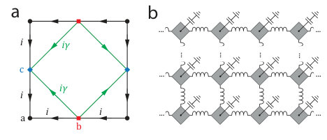 Figure 1
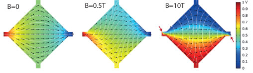 Figure 2
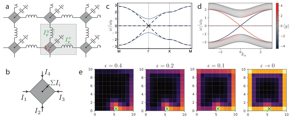 Figure 1
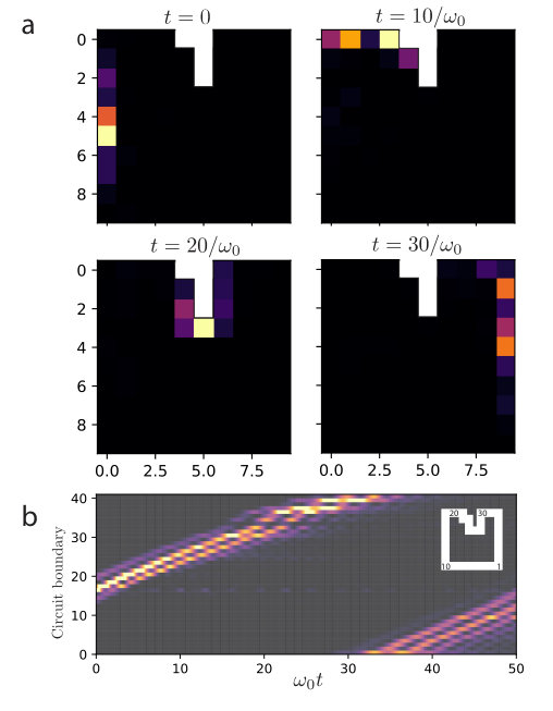 Figure 1
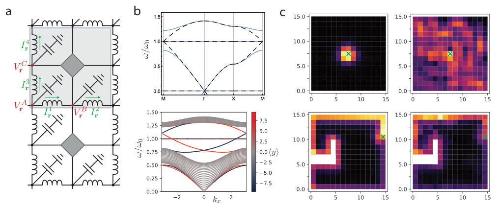 Figure 2
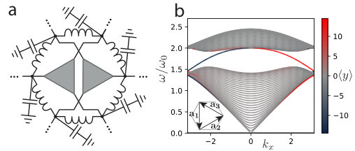 Figure 3
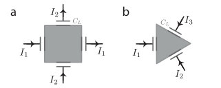 Figure 7
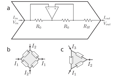 Figure 8
Peer Reviews
No public reviews on file for this paper yet. If you reviewed it on a platform where reviews are public (OpenReview, ICLR, NeurIPS, ICML), you can paste yours below so the community can read it here.
Videos
No videos yet. Explain this paper in a talk, walkthrough, or lecture? Add one.
Chern insulators for electromagnetic waves in electrical circuit networks
Rafael Haenel
Department of Physics and Astronomy, University of British Columbia, Vancouver, BC, Canada V6T 1Z1
Quantum Matter Institute, University of British Columbia, Vancouver BC, Canada V6T 1Z4
Timothy Branch
Department of Physics and Astronomy, University of British Columbia, Vancouver, BC, Canada V6T 1Z1
Quantum Matter Institute, University of British Columbia, Vancouver BC, Canada V6T 1Z4
Marcel Franz
Department of Physics and Astronomy, University of British Columbia, Vancouver, BC, Canada V6T 1Z1
Quantum Matter Institute, University of British Columbia, Vancouver BC, Canada V6T 1Z4
Abstract
Periodic networks composed of capacitors and inductors have been demonstrated to possess topological properties with respect to incident electromagnetic waves. Here, we develop an analogy between the mathematical description of waves propagating in such networks and models of Majorana fermions hopping on a lattice. Using this analogy we propose simple electrical network architectures that realize Chern insulating phases for electromagnetic waves. Such Chern insulating networks have a bulk gap for a range of signal frequencies that is easily tunable and exhibit topologically protected chiral edge modes that traverse the gap and are robust to perturbations. The requisite time reversal symmetry breaking is achieved by including a class of weakly dissipative Hall resistor elements whose physical implementation we describe in detail.
I Introduction
Topological states of matter in electronic systems exhibit topologically non-trivial bulk band structures accompanied by protected edge or surface modes Hasan and Kane (2010); Qi and Zhang (2011); Franz and Molenkamp (2013). More generally, the insights gained from the study of electrons in crystalline solids with non-trivial topology can be applied to any physical system whose degrees of freedom are governed by a wave equation. If bulk solutions of the wave equation do not exist in some range of frequencies, the system may be viewed as insulating for these frequencies and may in addition possess topologically protected propagating modes at its boundary. This realization has led to a theoretical study and physical implementation of a wide variety of periodic systems in which topological properties analogous to electronic topological insulators, superconductors and semimetals are manifest. Most prominent examples of these efforts include photonic Haldane and Raghu (2008); Lu et al. (2014), acoustic Prodan and Prodan (2009); Yang et al. (2015), mechanical Kane and Lubensky (2014); Huber (2016); Barlas and Prodan (2018), polaritonic Karzig et al. (2015), and electrical systems Ningyuan et al. (2015); Lee et al. (2018); Zhao (2018); Luo et al. (2018a).
In the present work, we focus on the latter class of topological systems, more specifically, periodic networks comprised of inductors, capacitors and resistors. These structures, also referred to as topoelectrical circuits Lee et al. (2018), have been demonstrated to possess topological properties with respect to the incident electromagnetic (EM) wave signals. In close analogy to electronic tight-binding models, various circuit models realizing classical analogs of quantum spin Hall states Ningyuan et al. (2015); Zhu et al. (2018), Dirac and Weyl semimetalsLee et al. (2018); Lu et al. (2018) and higher order topological insulatorsEzawa (2018a, b); Imhof et al. (2018) have been proposed and some of them have been experimentally characterized.
Conspicuously absent from this list is the Chern insulator – the analog of the most basic electronic topological phase, the quantum Hall insulator in two dimensions Haldane (1988). The reason is simple: networks composed of capacitors and inductors are governed by Maxwell equations which are fundamentally invariant under the time reversal operation . A Chern insulator, on the other hand, requires broken symmetry.
We note that ordinary resistors in a LC network cause dissipation and therefore break . This to some extent hinders the comparison to isolated quantum systems where dynamics are unitary. More importantly, -breaking produced by purely dissipative dynamics does not help in creating a Chern insulator. On the other hand dissipative networks can provide useful examples of systems studied in the rapidly advancing field of non-Hermitian quantum mechanics Shen et al. (2018); Gong et al. (2018); Luo et al. (2018b); Moiseyev (2011).
Here, we circumvent this problem by employing a class of weakly dissipative Hall resistors. These are linear circuit elements whose voltage response to a longitudinal current is predominantly transverse. An ideal Hall resistor introduces strong breaking into the circuit without significant dissipation and thus enables construction of the Chern insulator.
The class of EM Chern insulators we introduce here has a bulk gap for EM waves in a range of frequencies but exhibits chiral propagating edge modes that are gapless and traverse the gap. The edge modes are topologically protected by a non-zero Chern number defined by the bulk band structure of the network and are robust against any imperfections in the network that do not close the gap.
We discuss several specific network architectures that lead to the physics described above. We do this by taking advantage of a novel mapping that connects the dynamics of a certain class of periodic RLC networks to Hermitian Bloch Hamiltonians describing Majorana fermions in a crystal lattice. Such Hamiltonians are well known to possess Chern-insulating phases. While the possibility of non-trivial topological structure of Kirchhoff’s equations has been previously recognized, it is usually discussed in terms of admittance bands or mapped onto non-Hermitian eigenvalue problems Ningyuan et al. (2015); Lee et al. (2018). The description developed in this work offers a more direct analogy to crystalline solids and thus a more transparent physical interpretation in terms of well understood topological band theoryHasan and Kane (2010); Qi and Zhang (2011); Franz and Molenkamp (2013).
The key physical element required in the realization of our EM Chern insulator architecture is the Hall resistor. A natural implementation of the Hall resistor relies on the classical Hall effect in a clean metal or doped semiconductor film in applied perpendicular magnetic field with galvanic contacts. We will see that this simplest realization does not quite work and discuss an alternate setup with capacitive couplings. We also discuss implementations where near-ideal Hall response can be simulated using simple circuits with active elements: operational amplifiers. We conclude that these offer the most practical route towards the realization of Chern insulating networks that would function at room temperature and use only ready-made components.
II Chern insulators from RLC networks
II.1 General setup and a toy model
The simplest RLC network capable of exhibiting non-trivial topology is depicted in Fig. 1(a). It consists of an array of 5-terminal Hall elements, denoted by grey diamonds, arranged in a square lattice. The central terminal of each Hall element is connected to ground via a capacitor while the side terminals connect to neighboring Hall resistors through inductors .
The 5-terminal Hall element is characterized by its resistance tensor , defined by the relation
[TABLE]
Here, the voltages are measured with respect to the central terminal and the directionality of currents is indicated in Fig. 1(b). We note that Eq. (1) is the most general parametrization of under 4-fold rotational symmetry.
The description of the EM signal propagating through the circuit requires the definition of three dynamical variables: voltage across each capacitor, and two currents and flowing through the inductors in each unit cell labeled by vector . They are denoted by red and green labels in Fig. 1(a), respectively. Then, Kirchhoff laws yield the following coupled system of linear differential equations:
[TABLE]
The first of these equations expresses current conservation for each Hall element and the remaining two relate the voltage differences between neighboring unit cells to the corresponding currents through the usual constitutive relations for inductors and resistors. is a vector of currents flowing into the Hall resistor at position .
We begin by considering the case of a non-resistive network, i.e. . Then Eqs. (2) exhibit invariance under which sends and reverses all currents, . In addition, because voltages and currents are by definition real-valued, Eqs. (2) are trivially invariant under complex conjugation.
Eqs. (2) can be recast in the form of a Schrödinger equation with the wavefunction containing voltages and currents and the Hermitian Hamiltonian matrix. We can further exploit translational invariance of the network by expanding currents and voltages in terms of plane waves
[TABLE]
where and the rescaling is made for convenience. Equations (2) reduce to a Hermitian eigenvalue problem , where
[TABLE]
and .
is formally identical to a tight-binding model of Majorana fermions on the Lieb lattice. The effective electronic unit cell with imaginary hopping parameters is sketched in Fig. 2(a). The correspondence with Majorana as opposed to complex fermions follows from the fact that the original wave equation (2) is purely real-valued as is the time-domain Schrödinger equation for Majorana fermionsAlicea (2012); Beenakker (2013); Elliott and Franz (2015). We discuss this correspondence more fully in Appendix A.
The spectrum of consists of one zero mode , and two non-zero eigenvalues of the form
[TABLE]
It can be checked that the states belonging to the eigenvalue correspond to static patterns of currents in the network consistent with current conservation and zero voltages. These will be damped in the presence of arbitrary resistance and are of no interest to us. The two branches in Eq. (5) define the propagating modes of the system. They are gapless and linearly dispersing near , as illustrated in Fig. 1(c). Only the positive-frequency branch is physical; the negative branch appears because the ansatz in Eq. (3) permits complex-valued solutions while voltages and currents are strictly real.
In the Bloch Hamiltonian formulation time reversal symmetry and charge conjugation symmetry may be expressed as
[TABLE]
with . Both and square to and thus define the BDI class in the Altland-Zirnbauer classification Altland and Zirnbauer (1997). In two spatial dimensions class BDI supports only topologically trivial gapped phases Schnyder et al. (2008). Therefore, we must break time reversal symmetry to enable a topological phase in this system. (The symmetry derives from real-valuedness of Eq. (2) and therefore, like the analogous symmetry present in a generic superconductor, cannot be broken by a physical perturbation.) When is broken, the system belongs to class D which has an integer topological classification in . The corresponding topological invariant is the Chern number and its non-zero values label distinct Chern insulating phases.
To proceed, we now include a non-zero resistance tensor defined by Eq. (1). The Bloch Hamiltonian describing the network becomes
[TABLE]
with
[TABLE]
Time-reversal is explicitly broken whenever is non-zero. We observe that the Hamiltonian (7) remains Hermitian only when and both vanish for all . This requires and . Under these conditions the resistance tensor (1) becomes purely off-diagonal and antisymmetric. This form signifies a purely transverse, non-dissipative response – an “ideal Hall resistor”.
It is important to note that the resistance tensor, Eq. (1), is not invertible in this limit. As a consequence, the current response to applied voltages is ill-defined. However, we can still achieve sensible results by keeping a small non-zero dissipative components . This causes the network Hamiltonian to become non-Hermitian and results in weak damping of the AC signal. Topological properties of the system should not be affected as we explicitly illustrate below. Large non-Hermitian components could lead to new interesting topological phases and will be discussed elsewhere.
We now focus on the approximately Hermitian limit and define the Hall parameter . The bulk spectrum corresponding to the Hamiltonian (7) is illustrated in Fig. 1(c). It develops a gap measured in units of at . Since the term , responsible for the gap formation, is odd under time reversal, we expect the gapped phase to be topologically non-trivial. An explicit calculation indeed indicates a non-zero Chern number for the negative frequency band. Numerical calculation of the spectrum in a strip geometry confirms the existence of a single chiral edge mode traversing the gap, as shown in Fig. 1(d).
Experimental characterization of a finite size network can be given through the two-point impedance measurement which is conveniently described by the circuit Green’s function formalism. Here we give a brief review of the formalism while a more detailed discussion can be found e.g. in Ref. Lee et al., 2018. To begin one writes the frequency-domain Kirchhoff law for current conservation in the matrix form
[TABLE]
which defines the admittance tensor . The eigenmode spectrum can be calculated from the condition , which yields results equivalent to Eq. (5). The circuit Green’s function describes the voltage response of the network at point to a driving current profile according to
[TABLE]
In analogy to condensed matter systems, where the complete characterization of a non-interacting system is contained in the two-point correlation function , full experimental knowledge of provides a complete characterization of the electrical circuit. We can therefore expect topologically non-trivial behavior to be evident in a circuit’s two-point impedance.
In Fig. 1(e) we demonstrate this explicitly by plotting the voltage profile induced by a current with frequency injected at the boundary of a network. As an example of possible dissipative dynamics we include a non-zero component of the resistance tensor and quantify the strength of dissipation by a dimensionless parameter . For the frequency inside the bulk bandgap the signal is seen to propagate along the boundary of the system and in one direction only, consistent with the chiral nature of the gapless edge mode. Parameter clearly controls the lengthscale over which the signal is damped.
Finally, we investigate the propagation of such signals in the time domain. To this end we excite a Gaussian wave packet with the frequency width spatially localized around an edge site and unitarily evolve it in time with the propagator . The corresponding simulation for a non-dissipative network with and assuming randomness in and values is shown in Fig. 3(a). The edge signal propagates unidirectionally along the circuit boundary, even in the presence of boundary defects. A plot of the current at the network boundary as a function of time in Fig. 3(b) reveals approximately constant group velocity of the wave packet.
The circuit described above illustrates the mathematical correspondence between periodic RLC networks and tight-binding Hamiltonians with non-trivial topology. Our approach allows for the mapping of the differential equations governing the RLC network onto a simple Bloch equation known in the condensed-matter literature Weeks and Franz (2010). The non-trivial ingredient required to break time reversal symmetry is the 5-terminal Hall element described by the resistance tensor, Eq. (1). However, as we will discuss in Sec. III, its experimental realization is not straightforward. For this reason, we may regard the above network as an instructive but unphysical toy model. Below we will describe two different network architectures which have well-defined experimental implementations and are only slightly more complex.
II.2 Chern insulator on the square lattice
Consider the network depicted in Fig. 4(a). It has a square lattice symmetry and contains 4 inductors, 3 capacitors and one Hall resistor per unit cell. The Hall resistor is now in a 4-terminal configuration. We characterize it by the Hall admittance tensor that relates input currents to terminal voltages via . In its idealized version it is
[TABLE]
Currents and voltages are labeled as shown previously in Fig. 1(b) with the difference that no central terminal exists. We note that has rank 2 and is therefore not invertible. We can reduce (11) to a set of two linearly independent equations by realizing that it conserves current for pairs of opposing terminals, that is, for any voltage input the currents satisfy and . In electrical circuit theory this is known as the port condition. Two opposing terminals define a port. A full description of the Hall element is then achieved in terms of two currents through the ports, and , and two voltages across the ports, and . The corresponding resistance tensor is
[TABLE]
We note that the circuit element corresponding to the above resistance matrix is in fact well known in electrical engineering literature as the gyrator Tellegen (1948). This device, together with the resistor and the capacitor, defines a basis of linear circuit elements. All other network elements can be composed from the aforementioned three.
The degrees of freedom describing the network in Fig. 4(a) can be chosen as three voltages on the capacitors and four currents flowing through the inductors, forming a 7-component vector . To preserve the 4-fold rotation symmetry of the network, we take capacitances on B and C sublattices to be equal, , and further set with a dimensionless parameter. All inductors have inductance .
The corresponding Bloch Hamiltonian follows from current conservation for all nodes and Kirchhoff’s second law for the potential difference between two nodes connected through an inductor. It can be represented as a matrix of the form
[TABLE]
where is a matrix with all elements zero and denotes the matrix
[TABLE]
The matrix contains time reversal breaking terms due to presence of the the Hall element,
[TABLE]
with .
The mode spectrum of the circuit consists of 7 bands. Charge-conjugation symmetry constraints the bands to come in pairs of opposite frequency and the unpaired band to be confined to . In the absence of the Hall resistor time reversal symmetry enforces degeneracies at and as follows
[TABLE]
Here, we have defined . The Hall resistor breaks and splits the degeneracy at . The quadratic band crossing thus acquires a gap and the two bands become topologically non-trivial with the Chern number . Since the degeneracy at the point remains intact.
For an arbitrary and one thus expects the network to realize a Chern insulator. A situation of special interest occurs for . In the absence of the Hall resistor three bands then touch at and the middle band is completely flat, Fig. 4(b). The Hall resistor separates the three bands and makes the top and bottom bands topological with Chern number . The flat band remains trivial with . This is confirmed by numerical diagonalization of Hamiltonian Eq. (13) on a strip geometry with translational invariance along , shown in Fig. 4(b). We clearly observe chiral edge modes.
We further analyze the admittance properties of the network by calculating the circuit Green’s function in a finite system and plotting the voltage response to a current injected at a single node. For these calculations, we assume that the inductors are weakly resistive and characterize their resistance by a parameter . The resulting Hamiltonian becomes weakly non-Hermitian and the propagating waves are damped.
The upper left panel of Fig. 4(d) shows the response to a current of frequency within the gap that is injected at a bulk site. The voltage profile is localized around the node of injection. If we tune the frequency out of the bulk gap, the voltage signal propagates through the whole circuit, independent of the point of injection, as shown in the upper right panel. To demonstrate the topological nature of the edge transport, we include a defect on the circuit’s left boundary and excite the edge mode of the circuit at an in-gap frequency (bottom panels). As expected the signal propagates around the defect by following the distorted edge. This does not change qualitatively when we introduce bulk disorder, which we model by including a randomness in , , , and values, larger than typical tolerances of commercially available electronic components.
II.3 Chern insulator on the honeycomb lattice
The graph structure of RLC networks in principle allows for engineering arbitrary lattice models. Here, we briefly discuss a circuit whose tight-binding analog is similar the Haldane model on the honeycomb lattice Haldane (1988) which was historically the first model realizing the Chern insulator in electronic systems. A unit cell is schematically shown in Fig. 5(a). Each of the two sublattices of the honeycomb lattice contains a node that is connected to ground through a capacitor . Nearest-neighbor nodes are connected by inductors . Second neighbors within a hexagonal plaquette each connect to a three-terminal Hall resistor.
The three-terminal Hall resistor is described by a three-fold rotation symmetric resistance tensor whose idealized, non-dissipative form is defined by the relation
[TABLE]
While above resistance tensor is formally equivalent to the matrix in Eq. (12), the port condition does not apply for a triangular Hall element. Instead relates input currents at two of the three terminals to the corresponding terminal voltages. The potential at the third terminal is set to zero and the corresponding current is determined by current conservation.
The network in Fig. 5(a) has a tight-binding representation and topological structure closely related to Haldane’s celebrated lattice model of the Chern insulatorHaldane (1988). The Bloch Hamiltonian is a matrix which takes the same form as Eq. 13, where now
[TABLE]
Here, and are Bravais lattice vectors as shown in the inset of Fig. 4(b). Similar to graphene the band structure has a pair of Dirac points located at the corners of the hexagonal Brillouin zone but they now occur at non-zero frequency. The band crossings are protected by a combination of and the lattice inversion symmetry. Inclusion of the Hall resistors breaks and creates a Chern insulator. Numerical diagonalization of the Hamiltonian in the strip geometry confirms the existence of the chiral edge modes traversing the gap, Fig. 5(b).
III Hall resistor implementation
Non-trivial physics in the models studied in Sec. II above relies on Hall resistors characterized by a transverse voltage response to a longitudinal current that is odd under time reversal. Naively, the most straightforward realization of such devices exploits the classical (or quantum) Hall effect. Consider a 2D metal or semiconductor film in a perpendicular magnetic field. In the strong field limit current flows along equipotential lines yielding dissipationless transport. However, this picture neglects the influence of the boundaries of the Hall resistor. As we explicitly demonstrate in Appendix B, the boundaries give rise to a dissipative contact resistanceWick (1954). It is therefore impractical to realize a circuit described by a Hermitian eigenvalue problem in this manner. A possible workaround relies on capacitively coupling the Hall elements to the circuitViola and DiVincenzo (2014). We describe this effort in Appendix B and conclude that while it might work in principle a practical implementation is not straightforward.
On the other hand, 4-terminal Hall resistors that satisfy the port condition are well known among electrical engineers as “gyrators” and various other implementations have been conceived Hogan (1952); Shenoi (1965); Fabre (1992); Castellanos-Beltran et al. (2009); Koch et al. (2010). A notable example is the realization using operational amplifiers. Such gyrating circuits are discussed in standard textbooks Chua et al. (1987).
Here we describe a specific realization of the simulated ideal Hall resistor inspired by the recent work of Hofmann et al. Hofmann et al. (2018). It can be used in either 4- or 3-terminal configuration required for the Chern insulating networks discussed in Secs. IIB and IIC, but not in the 5-terminal configuration. Construction of the Hall element is based on the building block depicted in Fig. 6(a). It consists of an operational amplifier and three resistors. A derivation of the corresponding admittance tensor is given in Appendix A of Ref. Hofmann et al., 2018. It is
[TABLE]
where currents and voltages are defined as in Fig. 6(a). Remarkably, arranged in a two-port configuration as depicted in Fig. 6(b) or three-terminal configuration in Fig. 6(c), these elements precisely realize the respective ideal Hall resistors required for our proposed Chern insulator networks.
Operational amplifiers are commercially available at low cost and can operate in a wide range of frequencies, voltages and power settings. Experimental realization of the Chern-insulating networks using the simulated Hall elements depicted in Fig. 6 should therefore be easily achievable.
IV Summary and outlook
In this work, we proposed periodic RLC networks that function as Chern insulators for electromagnetic signals in a broad range of frequencies tunable by adjusting the values of inductance , capacitance and Hall resistance of the circuit elements. The design is guided by exploiting an analogy between equations governing the EM fields in periodic RLC networks and tight-binding models for Majorana fermions which are known to possess topologically non-trivial phases. Our approach maps the Kirchhoff’s laws describing the network onto a Hermitian eigenvalue problem in the crystal momentum space where the eigenvalues correspond to frequency modes of the network. Topological properties of the network are then inferred transparently in direct analogy to condensed matter Hamiltonians.
Explicitly, we have proposed three different network architectures realizing Chern insulating phases for EM signals. The required time reversal symmetry breaking is achieved by including Hall resistors which are non-reciprocal circuit elements also known in engineering literature as gyrators. These may be implemented as capacitively contacted metallic or semiconductor films in an external magnetic field or as simple circuits with resistors and off-the-shelf operational amplifiers. In the latter implementation the time reversal symmetry is broken by the external source of power required to operate the amplifiers. Nevertheless, due to the feedback structure the operational amplifiers are operated in the linear response regime and the simulated Hall devices can be regarded as linear circuit elements.
Topological properties of the networks proposed in this work are manifest in the chiral edge modes traversing the gap in the bulk spectrum. These edge modes give rise to unidirectionally propagating voltage and current signals along the network boundary. They are topologically protected by the bulk topological invariant (the integer Chern number) and cannot be removed by any deformation of the boundary. In addition, the edge modes are robust against moderate amount of bulk disorder, as realized e.g. by a random spread in the parameters characterizing the individual network elements.
Chern insulating EM networks provide a highly tunable experimental environment. Scale invariance of Maxwell’s equations allows for engineering of band gaps and edge modes in a wide frequency range. Moreover, the flexible graph nature of such networks removes any restriction on dimensionality or locality. Consequently, exotic synthetic materials of arbitrary dimension and connectivity may be designed. In addition to possible engineering applications, Chern insulating EM networks may be established as a teaching resource in university laboratory courses and demonstrations.
Acknowledgments.– We thank Doug Bonn, Sarah Burke, Gil Refael and Ronny Thomale for helpful discussions. Research described in this article was supported by NSERC and by CIFAR. Software that facilitated this research was provided by CMC Microsystems. M.F. acknowledges the hospitality of The Aspen Center for Physics and KITP Santa Barbara where part of this work was completed.
Note added. – When this work was essentially completed we learned about a related proposal for a Chern-insulating LC network with operational amplifiers serving as -breaking elements Hofmann et al. (2018). We have subsequently added a brief discussion in Sec. III.
Appendix A Relation to Majorana tight-binding models
A general model for non-interacting Majorana fermions on a lattice is defined by a Hamiltonian of the form
[TABLE]
Here are Majorana operators satisfying the canonical anticommutation relations
[TABLE]
and is an matrix of tunneling amplitudes between lattice sites and (we assume the lattice has sites.). Hermiticity of together with relations (22) imply that is purely imaginary and antisymmetric. We henceforth write it as where is a real antisymmetric matrix.
Solving the problem defined by Hamiltonian (21) is equivalent to diagonalizing matrix . Time evolution of an arbitrary state is then governed by the corresponding Schrödinger equation
[TABLE]
where is regarded as an -component state vector in the site basis. Using the property we see that Eq. (23) becomes a purely real-valued wave equation which, therefore, admits purely real solutions .
It is this property of Majorana tight-binding models that motivates the connection to electrical networks which are also governed by real-valued wave equations, like Eq. (2). As an example it is an easy exercise to show that Majorana fermions on the Lieb lattice with tunneling amplitudes illustrated in Fig. 2(a) are described by the same Hamiltonian as the RLC circuit discussed in Sec. IIA.
Appendix B Hall-resistor implementation by classical Hall effect
B.1 Hall effect, galvanic coupling
We consider a metal or semiconductor film in a perpendicular magnetic field . In such a setting the microscopic current response is accurately described by Ohm’s law, , where the material’s conductivity takes the form Ashcroft and Mermin (1976)
[TABLE]
Here, is the zero-field conductivity and is the Hall coefficient. For , the microscopic current response to a potential gradient is predominantly transverse so one might think that a device depicted in Fig. 7 could serve as a near-ideal Hall resistor. As our simulations below illustrate, this unfortunately is not the case because of the phenomenon of geometric magnetoresistanceWick (1954).
We use Comsol Multiphysics finite element software to numerically solve the current conservation equation for the 4-terminal geometry depicted in Fig. 7. We choose insulating boundary conditions for the edges as well as top and bottom terminals and drive a longitudinal current by a voltage difference from the left to the right terminal. The resulting potential distribution is plotted as a colorscale, electric field lines are white, and the current flow is denoted by black arrows. For , the current flow is parallel to and the potential difference between top and bottom terminals is . As one increases the magnetic field, and span the Hall angle and one measures a finite Hall voltage . For constant current flow, increases linearly with . Naively, one could expect that for large enough field . This is the necessary condition for the realization of an ideal Hall element. However, as one can see in the right panel of Fig. 7, the Hall voltage saturates at .
This effect is commonly known as two-terminal resistance and may be interpreted as a geometrical magnetoresistance. For the diamond geometry it establishes a linear magnetic field dependence of the longitudinal resistance. For constant current, and then show the same linear behavior at high fields, precluding the desired limit . In fact, it has been shown that, on general grounds, for arbitrarily shaped 3-, 4-, and 6-terminal geometry and arbitrary magnetic fieldWick (1954).
It may seem puzzling that a Hall element is dissipative in the limit . After all the dissipated power is and should vanish when . But can still be non-zero if the electric field strength diverges at some point in the sample. In fact, it is known that the two-terminal resistance arises at two points near the terminals where the boundary conditions change from galvanic to electrically insulating. At these points, the electric field diverges. In our setup the points with divergent field strength are marked by red arrows in the rightmost panel of Fig. 7.
B.2 Hall effect, capacitive coupling
Viola and DiVincenco Viola and DiVincenzo (2014) proposed an elegant way to circumvent the problem of diverging electric fields outlined above. They showed that a near ideal Hall resistor can be achieved by replacing galvanic contacts by capacitive coupling to the terminals. The resulting setup, illustrated in Fig. 8, yields solutions of the EM field equations that are well behaved on the whole resistor geometry. Explicitly, their resulting impedance tensor for a 2-port geometry Fig. 8(a) in the limit has the form
[TABLE]
Here, is the capacitance of a single contact, which are assumed to be the same for simplicity. The anti-symmetric structure of the tensor implies that no energy is dissipated. For a discrete set of perfect “gyration” frequencies
[TABLE]
diagonal elements vanish and the above tensor describes an ideal Hall resistor.
The impedance tensor of the capacitively contacted Hall element is intrinsically dependent on the drive frequency and this dependence is fundamentally non-linear. This prevents a description in terms of the Bloch equation with a simple frequency-independent Hamiltonian but one can still use the circuit Green’s function method to describe a periodic LC network with these elements. We have checked numerically that the capacitively coupled Hall element can indeed be used in network architectures discussed in Secs. IIB and IIC and that it produces Chern insulators, provided that the first gyration frequency Eq. (28) is tuned close to the frequency of the band crossing where one wants to open a gap. This is not surprising given that at the impedance tensor coincides with the resistance tensor assumed in Secs. IIB and IIC, Eq. (12).
Simple physical description of the Viola-DiVincenco setup that gives Eq. (27) relies on the dynamics of the magnetoplasmon edge mode in the Hall effect deviceViola and DiVincenzo (2014). It will work equally well in the 4- and 3-terminal configuration, but the 5-terminal configuration that is required for our toy model analyzed in Sec. IIA cannot be realized in this manner.
The reference list from the paper itself. Each links out to its DOI / PubMed record.
- 1Hasan and Kane (2010) M. Z. Hasan and C. L. Kane, Reviews of Modern Physics 82 , 3045 (2010) . · doi ↗
- 2Qi and Zhang (2011) X.-L. Qi and S.-C. Zhang, Reviews of Modern Physics 83 , 1057 (2011) . · doi ↗
- 3Franz and Molenkamp (2013) M. Franz and L. Molenkamp, Topological Insulators. (Elsevier Science, Burlington, 2013).
- 4Haldane and Raghu (2008) F. D. M. Haldane and S. Raghu, Phys. Rev. Lett. 100 , 013904 (2008) . · doi ↗
- 5Lu et al. (2014) L. Lu, J. D. Joannopoulos, and M. Soljačić, Nature Photonics 8 , 821 (2014) . · doi ↗
- 6Prodan and Prodan (2009) E. Prodan and C. Prodan, Physical Review Letters 103 , 248101 (2009) . · doi ↗
- 7Yang et al. (2015) Z. Yang, F. Gao, X. Shi, X. Lin, Z. Gao, Y. Chong, and B. Zhang, Physical review letters 114 , 114301 (2015) . · doi ↗
- 8Kane and Lubensky (2014) C. L. Kane and T. C. Lubensky, Nature Physics 10 , 39 (2014) . · doi ↗