Maskless laser processing of graphene
Fujio Wakaya, Tadashi Kurihara, Nariaki Yurugi, Satoshi Abo, Masayuki, Abe, Mikio Takai

TL;DR
This paper demonstrates a maskless laser technique to selectively remove and pattern graphene on substrates, with control based on graphene thickness, using ultraviolet pulsed laser irradiation.
Contribution
It introduces a novel maskless laser process for thickness-selective removal and patterning of graphene on SiO2/Si substrates.
Findings
Threshold laser power depends on graphene thickness.
Thickness-dependent removal enables selective patterning.
Maskless laser patterning in air is feasible.
Abstract
Graphene on a SiO/Si substrate was removed by ultraviolet pulsed laser irradiation. Threshold laser power density to remove graphene depended on the graphene thickness. The mechanism is discussed using kinetic energy of thermal expansion of the substrate surface. Utilizing the thickness dependence, thickness (or layer-number) selective process for graphene is demonstrated. Maskless patterning of graphene using laser irradiation in the air is also demonstrated.
Click any figure to enlarge with its caption.
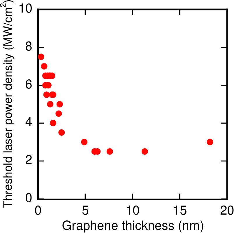 Figure 1
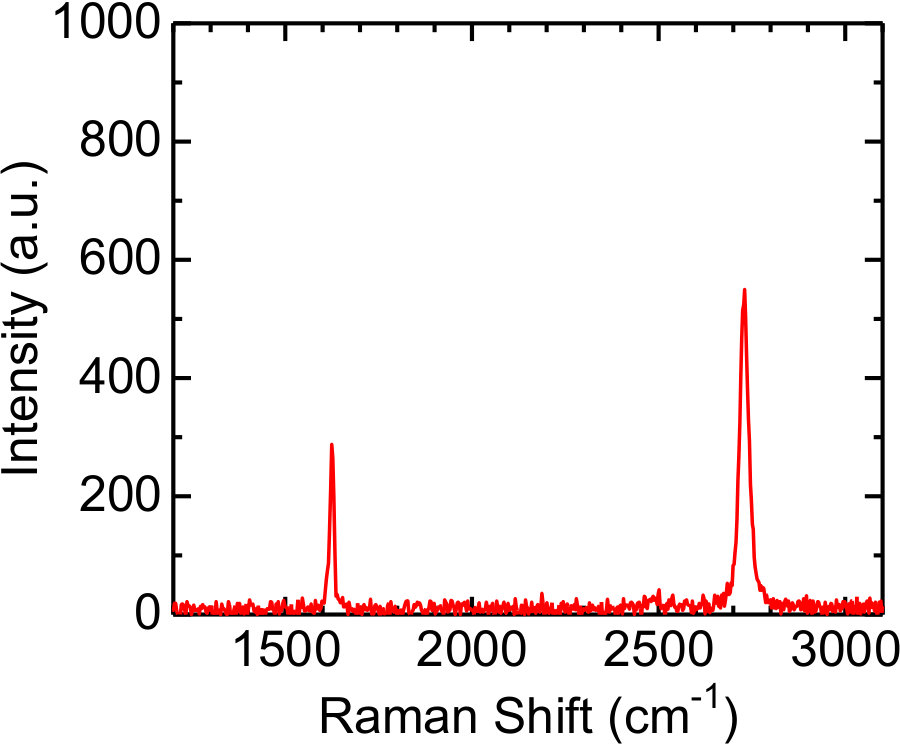 Figure 2
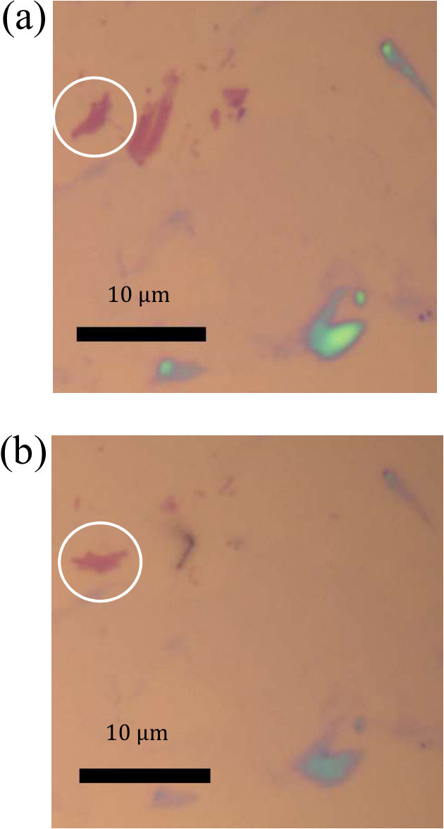 Figure 3
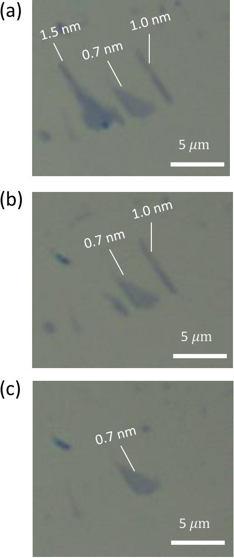 Figure 4
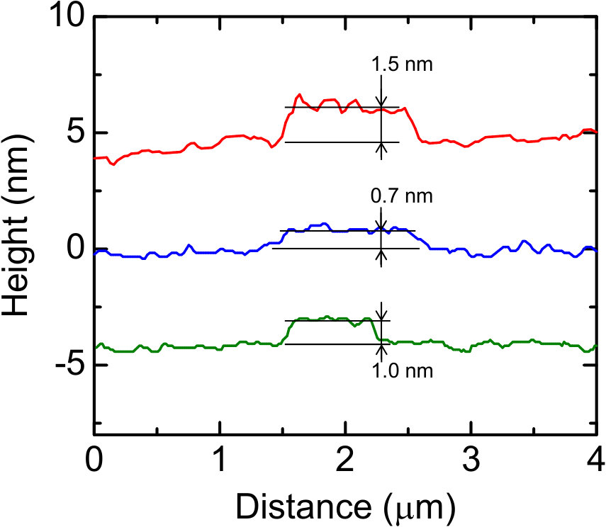 Figure 5
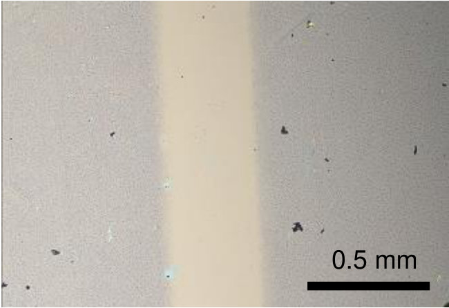 Figure 6
Peer Reviews
No public reviews on file for this paper yet. If you reviewed it on a platform where reviews are public (OpenReview, ICLR, NeurIPS, ICML), you can paste yours below so the community can read it here.
Videos
No videos yet. Explain this paper in a talk, walkthrough, or lecture? Add one.
Maskless laser processing of graphene
Fujio Wakaya
Center for Science and Technology at Extreme Conditions, Graduate School of Engineering Science, Osaka University 1-3 Machikaneyama, Toyonaka, Osaka 560-8531, Japan
Tadashi Kurihara
Center for Science and Technology at Extreme Conditions, Graduate School of Engineering Science, Osaka University 1-3 Machikaneyama, Toyonaka, Osaka 560-8531, Japan
Nariaki Yurugi
Center for Science and Technology at Extreme Conditions, Graduate School of Engineering Science, Osaka University 1-3 Machikaneyama, Toyonaka, Osaka 560-8531, Japan
Satoshi Abo
Center for Science and Technology at Extreme Conditions, Graduate School of Engineering Science, Osaka University 1-3 Machikaneyama, Toyonaka, Osaka 560-8531, Japan
Masayuki Abe
Center for Science and Technology at Extreme Conditions, Graduate School of Engineering Science, Osaka University 1-3 Machikaneyama, Toyonaka, Osaka 560-8531, Japan
Mikio Takai
Center for Science and Technology at Extreme Conditions, Graduate School of Engineering Science, Osaka University 1-3 Machikaneyama, Toyonaka, Osaka 560-8531, Japan
(Oct. 24, 2014 submitted to Microelectronic Eng.; revised on Mar.10, 2015; accepted on Mar. 25, 2015)
Abstract
Graphene on a SiO2/Si substrate was removed by ultraviolet pulsed laser irradiation. Threshold laser power density to remove graphene depended on the graphene thickness. The mechanism is discussed using kinetic energy of thermal expansion of the substrate surface. Utilizing the thickness dependence, thickness (or layer-number) selective process for graphene is demonstrated. Maskless patterning of graphene using laser irradiation in the air is also demonstrated.
Keywords: graphene; maskless laser process; ultraviolet laser
Journal reference: Microelectronic Eng. 141, 203-206 (2015) (published online Apr. 2, 2015)
DOI: 10.1016/j.mee.2015.03.049
I Introduction
Graphene has been drawing attention due to the outstanding electrical and optical characteristics since the so-called scotch-tape method was used to transfer graphene from graphite.Novoselov et al. (2004) Although extremely high room-temperature carrier mobility in graphene may be utilized for a high-speed transistor, realizing such transistors is still a challenging issue due to such problems as band-gap control McCann (2006); Ohta et al. (2006) and mobility suppression by extrinsic scatterings.Bolotin et al. (2008a, b) Another most realistic application of graphene is a transparent electrode utilizing high transmittance and high electrical conductance of graphene. Graphene transparent electrodes have been reported in solar cells, touch screen panels, and flat panel displays,Wu et al. (2008); Kim et al. (2009); Li et al. (2009); Bae et al. (2010) which means that mass-production technology is one of the most important issues in this field presently.
Indium tin oxide (ITO) is widely used for the material of the transparent electrode. For patterning of ITO, maskless laser process using infrared or ultraviolet (UV) lasers was reported as a simple and fast process comparing to the conventional lithography process with a resist and masks.Takai, Bollmann, and Haberger (1994); Yavas and Takai (1998) The mechanism for the ITO etching by laser irradiation was reported to be high-temperature effects, i.e. melting, evaporation, and ablation.Takai, Bollmann, and Haberger (1994); Yavas and Takai (1998)
In the previous study,Wakaya et al. (2013) we reported that UV pulsed laser irradiation with a wavelength of 248 nm removed graphene from a SiO2/Si surface if the laser power density is over a threshold value, and that no thickness changes and no defect generations were observed below the threshold power density. Mechanism for the observed removal was supposed to be mechanical ejection from the substrate surface. Moreover, a possibility of selective removal of thick graphene was pointed out.
In this paper, graphene thickness dependence of the threshold laser power density is discussed, and the thickness-selective process using UV pulsed laser irradiation is demonstrated. Such a selective process should be quite useful because a specific-layer-number graphene is preferable for many applications. Furthermore, the maskless patterning of the graphene is also demonstrated.
II Experimental
For the experiments of determining the threshold laser power density to remove graphene from the substrate surface, a Si substrate covered with 100-nm-thick SiO2 layer was used. Graphene pieces were transferred onto the substrate surface from natural graphite using the scotch-tape process. The samples after the scotch-tape process were first observed by optical microscopy. The graphene thickness was determined by atomic-force-microscopy (AFM) observation and Raman spectroscopy with an incident laser wavelength of 488 nm. The samples were irradiated by KrF excimer laser with a wavelength and a pulse width of 248 nm and 20 ns, respectively. The laser beam was homogenized and shaped to a stripe (0.4 60 mm2). The repetition frequency of the pulsed laser was 30 Hz. The sample stage was moved at 0.6 mm/s to the direction of the 0.4-mm width of the stripe, resulting in 95% overlap between the successive two pulses and 20 pulse irradiations at every point on the sample. This overlap and the many irradiations are to avoid the influence of ununiform intensity in the stripe of the laser light. Accumulation of the laser irradiation effects cannot be expected because the laser pulse width of 20 ns is much shorter than the repetition cycle of 33 ms. After laser irradiation, the samples were again observed by optical microscopy. This procedure was repeated with higher laser power density until the graphene was removed. The laser power density at which the graphene was removed was defined as the threshold laser power density. The threshold laser power densities for many graphene pieces with various thicknesses were determined to obtain thickness dependence of the threshold power density.
For the demonstration of maskless patterning using laser irradiation, almost all setups were the same as described above except for the starting material and the sample stage control. Commercially available graphene-on-SiO2(100nm)/Si samples were used for this purpose. Almost all regions of the sample surface were covered by single-layer graphene, which was grown by the chemical vapor deposition and transferred onto the SiO2/Si substrate. The sample stage was not moved during the demonstration. A 0.4-mm-wide stripe pattern was, therefore, expected to appear by the demonstration.
III Results and discussion
Fig. 1 shows experimentally obtained graphene thickness dependence of the threshold laser power density for removing graphene from the substrate surface.
It is shown that the thinner graphene needs the higher laser power. While the AFM measurement was used to determine the graphene thickness, Raman spectroscopy was also used for very thin graphene to be regarded as single-layer graphene. Fig. 2 shows the Raman spectrum for the graphene identified as single-layer.Graf et al. (2007)
As discussed in the dry laser cleaning process,Arnold (2002) during the laser irradiation the substrate material is thermally expanded with a surface velocity, , of
[TABLE]
Here, is the Poisson ratio, is the thermal expansion coefficient, is the specific heat, is the density, and is the absorbed laser power density. Ignoring reflection of the laser light and absorption by the graphene, we can estimate the velocity to be 22 cm/s for 8.0 MW/cm2 laser irradiation. For the estimation, , K*-1*, J/gK, and g/cm3 are used for Si at 300 K Arnold (2002) although these parameters should depend on the temperature, and SiO2 is ignored because it is transparent for the 248-nm-wavelength light. The kinetic energy per unit area which the graphene could receive from the surface expansion can be estimated as , where is the sheet density of graphene. This energy is J/m2 for single-layer graphene for 8.0 MW/cm2 laser irradiation. The energy is proportional to the sheet density of graphene, which means that the thicker graphene can receive more energy from the substrate expansion. We believe that receiving this kinetic energy is the principal mechanism for the observed thickness dependence of the threshold laser power density.
The adhesion potential between graphene and a SiO2 surface was reported as J/m2,Koenig et al. (2011); Zong et al. (2010) which is measured at room temperature and seven orders of magnitude larger than the kinetic energy discussed above. The large discrepancy may be due to the temperature rise during the laser irradiation. When a laser light with a power density of I is absorbed by a thick Si substrate, the temperature T at the Si surface after time t is Toyoda (1990)
[TABLE]
where and are the thermal conductivity and thermal diffusivity of Si, respectively. Although the layer structure in the present work is different from the thick Si substrate without any other layers, the temperature at the graphene and the SiO2 layer can be estimated using Eq. (2) because the absorption at the thin graphene and the SiO2 layer can be ignored for a rough estimation. The temperature after 20 ns from 8.0 MW/cm2 irradiations is actually estimated to be 790 oC. For the estimation, W/mK National_Astronomical_Observatory_of_Japan (1990) and are used. The thermal vibration energy per each atom can be estimated as , which is J for 790 oC. The atom density of graphene is m*-2*. The thermal vibration energy per unit area is, therefore, J/m2, which is on the same order as the room-temperature adhesion potential between graphene and SiO2.Koenig et al. (2011); Zong et al. (2010) The estimated high temperature, therefore, might affect the adhesion potential effectively through the thermal vibration of the atoms. The absorption coefficient of the 248-nm-wavelength light for the graphite along the c axis and the corresponding absorption length are 0.13 nm*-1* and 7.7 nm, respectively,Borghesi and Guizzetti (1991) which means that relatively large absorption occurs at the graphene layer especially if the graphene is thick comparing to the absorption length. A numerical simulation taking the reflection at the top surface and the interface, the absorption at the graphene layer, the heat conduction at all layers and the thermal expansion of SiO2 and Si layers into account is necessary to discuss the thermal expansion and the temperature in more detail.
The authors in Ref. Dhar et al., 2011 also reported that the threshold laser energy depended on the graphene thickness, which is quite similar to the result in the present work. Their interpretation is, however, different from that in the present work. They argued that the mechanism for the graphene removal was thermal ablation and attributed the observed graphene thickness dependence to that the specific heat depends on the graphene thickness. They, however, observed that a part of the graphene edge was folded onto the graphene after laser irradiation. As a similar example, we observed that a graphene piece was found at a different position with a different rotation angle after laser irradiation as shown in Fig. 3. Such experimental observation suggests that the mechanism for the graphene removal is mechanical ejection from the surface. The large discrepancy of the estimated kinetic energy to the adhesion energy reported in the literature, however, may suggest that both of the mechanical and thermal effects should be considered.
The graphene thickness dependence of the threshold power density shown in Fig. 1 suggests a possibility of thickness (or layer-number) selective process. Fig. 4 shows a demonstration of such a process.
There are three graphene pieces with a thickness of 0.7 nm, 1.0 nm, and 1.5 nm as shown in Fig. 4(a). The AFM cross-sectional plots of the graphene pieces are shown in Fig. 5.
After 5.5 MW/cm2 laser irradiation, only the 1.5-nm-thick graphene was removed as shown in Fig. 4(b). The 1.0-nm-thick graphene was removed by the 6.5 MW/cm2 laser irradiation as shown in Fig. 4(c). As a result, only the thinnest graphene with a thickness of 0.7 nm remains on the substrate. This experiment successfully demonstrates the thickness selective process of the graphene by UV pulsed laser irradiation.
A demonstration result of the maskless patterning of graphene in the air by laser irradiation is shown in Fig. 6.
The central part of the single-layer graphene/SiO2/Si sample surface was irradiated by stripe-shaped laser light at 10 MW/cm2. The 0.4-mm-wide stripe where no graphene existed was clearly observed in the figure. If the laser light is shaped as a spot and the sample stage is computer-controlled, an arbitrary pattern can be realized by laser irradiation in the air without masks, which should be useful in the mass-production process. The graphene material used for the demonstration was not a huge single crystal but consisted of many pieces of grain, the size of which was typically several m. Possible mechanism for the demonstration is, therefore, that each piece of the graphene is ejected without breaking the covalent bond between the carbon atoms when the substrate is irradiated by the laser.
IV Summary
Graphene pieces on a SiO2/Si substrate were removed by UV pulsed laser irradiation. The threshold power density to remove graphene depended on the graphene thickness. The mechanism was proposed using the substrate thermal expansion as is well known in the dry laser cleaning process.
Utilizing the thickness dependence of the threshold laser power density, thickness selective process for graphene was demonstrated. The thickness selective process, or layer-number selective process, is quite interesting because a specific layer-number graphene is preferable in many applications.
Maskless patterning of graphene using laser irradiation in the air was demonstrated using a SiO2/Si substrate covered with single-layer graphene. This process will contribute to the mass production of graphene devices.
Acknowledgements.
The authors acknowledge financial support from the Japan Society for Promotion of Science with KAKENHI Grant Number 25420287.
References
- Novoselov et al. (2004) K. S. Novoselov, A. K. Geim, S. V. Morozov, D. Jiang, Y. Zhang, S. V. Dubonos, I. V. Grigorieva, and A. A. Firsov, Science 306, 666 (2004).
- McCann (2006) E. McCann, Phys. Rev. B 74, 161403 (2006).
- Ohta et al. (2006) T. Ohta, A. Bostwick, T. Seyller, K. Horn, and E. Rotenberg, Science 313, 951 (2006).
- Bolotin et al. (2008a) K. I. Bolotin, K. J. Sikes, J. Hone, H. L. Stormer, and P. Kim, Phys. Rev. Lett. 101, 096802 (2008a).
- Bolotin et al. (2008b) K. Bolotin, K. Sikes, Z. Jiang, M. Klima, G. Fudenberg, J. Hone, P. Kim, and H. Stormer, Solid State Commun. 146, 351 (2008b).
- Wu et al. (2008) J. Wu, H. A. Becerril, Z. Bao, Z. Liu, Y. Chen, and P. Peumans, Appl. Phys. Lett. 92, 263302 (2008).
- Kim et al. (2009) K. S. Kim, Y. Zhao, H. Jang, S. Y. Lee, J. M. Kim, K. S. Kim, J.-H. Ahn, P. Kim, J.-Y. Choi, and B. H. Hong, Nature 457, 706 (2009).
- Li et al. (2009) X. Li, Y. Zhu, W. Cai, M. Borysiak, B. Han, D. Chen, R. D. Piner, L. Colombo, and R. S. Ruoff, Nano Lett. 9, 4359 (2009).
- Bae et al. (2010) S. Bae, H. Kim, Y. Lee, X. Xu, J.-S. Park, Y. Zheng, J. Balakrishnan, T. Lei, H. R. Kim, Y. I. Song, Y.-J. Kim, K. S. Kim, B. Ozyilmaz, J.-H. Ahn, B. H. Hong, and S. Iijima, Nat. Nanotechnol. 5, 574 (2010).
- Takai, Bollmann, and Haberger (1994) M. Takai, D. Bollmann, and K. Haberger, Appl. Phys. Lett. 64, 2560 (1994).
- Yavas and Takai (1998) O. Yavas and M. Takai, Appl. Phys. Lett. 73, 2558 (1998).
- Wakaya et al. (2013) F. Wakaya, T. Kurihara, S. Abo, and M. Takai, Microelectron. Eng. 110, 358 (2013).
- Graf et al. (2007) D. Graf, F. Molitor, K. Ensslin, C. Stampfer, A. Jungen, C. Hierold, and L. Wirtz, Nano Lett. 7, 238 (2007).
- Arnold (2002) N. Arnold, in Laser Cleaning, edited by B. Luk’yanchuk (World Scientific, Singapore, 2002) p. 51.
- Koenig et al. (2011) S. P. Koenig, N. G. Boddeti, M. L. Dunn, and J. S. Bunch, Nat. Nanotechnol. 6, 543 (2011).
- Zong et al. (2010) Z. Zong, C.-L. Chen, M. R. Dokmeci, and K.-T. Wan, J. Appl. Phys. 107, 026104 (2010).
- Toyoda (1990) K. Toyoda, Laser Processing ed. the Laser Society of Japan [in Japanese] (Nikkei Gijutsu Tosho, Tokyo, 1990) pp. 19–32.
- National_Astronomical_Observatory_of_Japan (1990) National Astronomical Observatory of Japan, ed., Rika Nenpyo (Chronological Scientific Tables) [in Japanese] (Maruzen, Tokyo, 1990).
- Borghesi and Guizzetti (1991) A. Borghesi and G. Guizzetti, in Handb. Opt. Constants of Solids II, edited by E. D. Palic (Academic Press, San Diego, 1991) p. 449.
- Dhar et al. (2011) S. Dhar, A. R. Barman, G. X. Ni, X. Wang, X. F. Xu, Y. Zheng, S. Tripathy, A. Rusydi, K. P. Loh, M. Rubhausen, a. H. C. Neto, B. Őzyilmaz, and T. Venkatesan, AIP Adv. 1, 022109 (2011).
The reference list from the paper itself. Each links out to its DOI / PubMed record.
- 1Novoselov et al. (2004) K. S. Novoselov, A. K. Geim, S. V. Morozov, D. Jiang, Y. Zhang, S. V. Dubonos, I. V. Grigorieva, and A. A. Firsov, Science 306 , 666 (2004) . · doi ↗
- 2Mc Cann (2006) E. Mc Cann, Phys. Rev. B 74 , 161403 (2006) . · doi ↗
- 3Ohta et al. (2006) T. Ohta, A. Bostwick, T. Seyller, K. Horn, and E. Rotenberg, Science 313 , 951 (2006) . · doi ↗
- 4Bolotin et al. (2008 a) K. I. Bolotin, K. J. Sikes, J. Hone, H. L. Stormer, and P. Kim, Phys. Rev. Lett. 101 , 096802 (2008 a) . · doi ↗
- 5Bolotin et al. (2008 b) K. Bolotin, K. Sikes, Z. Jiang, M. Klima, G. Fudenberg, J. Hone, P. Kim, and H. Stormer, Solid State Commun. 146 , 351 (2008 b) . · doi ↗
- 6Wu et al. (2008) J. Wu, H. A. Becerril, Z. Bao, Z. Liu, Y. Chen, and P. Peumans, Appl. Phys. Lett. 92 , 263302 (2008) . · doi ↗
- 7Kim et al. (2009) K. S. Kim, Y. Zhao, H. Jang, S. Y. Lee, J. M. Kim, K. S. Kim, J.-H. Ahn, P. Kim, J.-Y. Choi, and B. H. Hong, Nature 457 , 706 (2009) . · doi ↗
- 8Li et al. (2009) X. Li, Y. Zhu, W. Cai, M. Borysiak, B. Han, D. Chen, R. D. Piner, L. Colombo, and R. S. Ruoff, Nano Lett. 9 , 4359 (2009) . · doi ↗