Characterization of X-ray charge neutralizer using carbon-nanotube field emitter
Shuhei Okawaki, Satoshi Abo, Fujio Wakaya, Hayato Yamashita, Masayuki, Abe, Mikio Takai

TL;DR
This paper demonstrates a carbon-nanotube based X-ray charge neutralizer, characterizing its X-ray output and charge neutralization performance, indicating potential for large-area flat-panel applications.
Contribution
It introduces a novel X-ray charge neutralizer using a carbon-nanotube field emitter and provides detailed characterization of its performance.
Findings
Good charge neutralization performance observed
X-ray yields and spectra characterized
Potential for large-area flat-panel neutralizers
Abstract
An X-ray charge neutralizer using a screen-printed carbon-nanotube field emitter is demonstrated to show the possibility of a large-area flat-panel charge neutralizer, although the device dimensions in the present work are not very large. The X-ray yields and spectra are characterized to estimate the ion generation rate as one of the figures of merit of neutralizers. Charge neutralization characteristics are measured and show good performance.
Click any figure to enlarge with its caption.
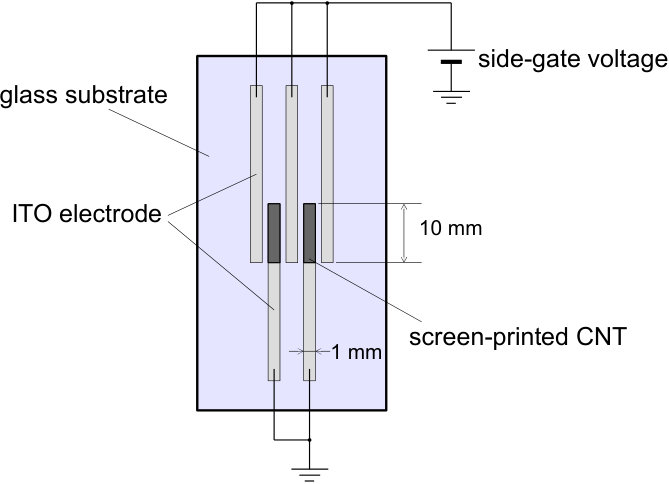 Figure 1
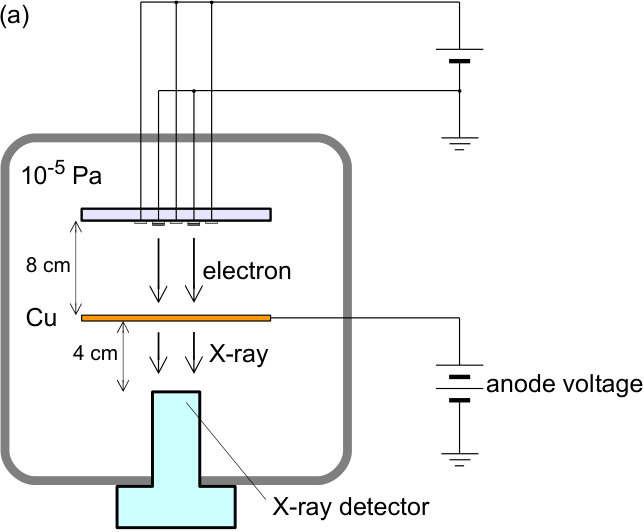 Figure 2
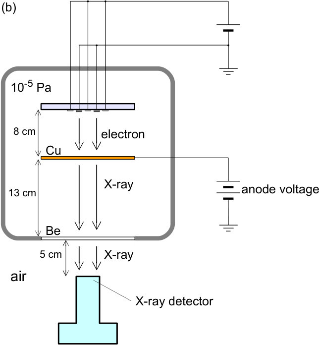 Figure 2
 Figure 3
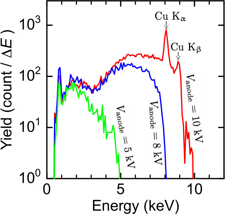 Figure 4
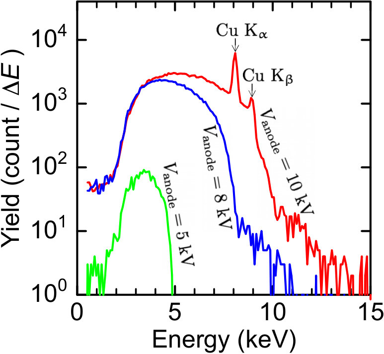 Figure 5
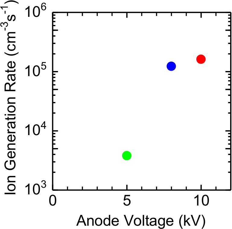 Figure 6
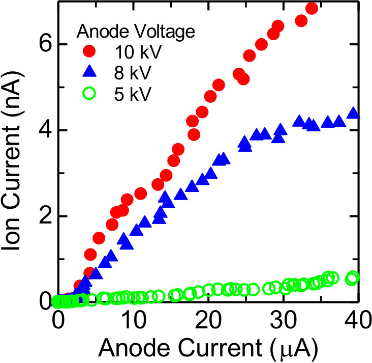 Figure 7
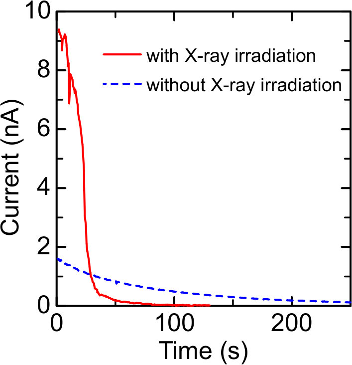 Figure 8
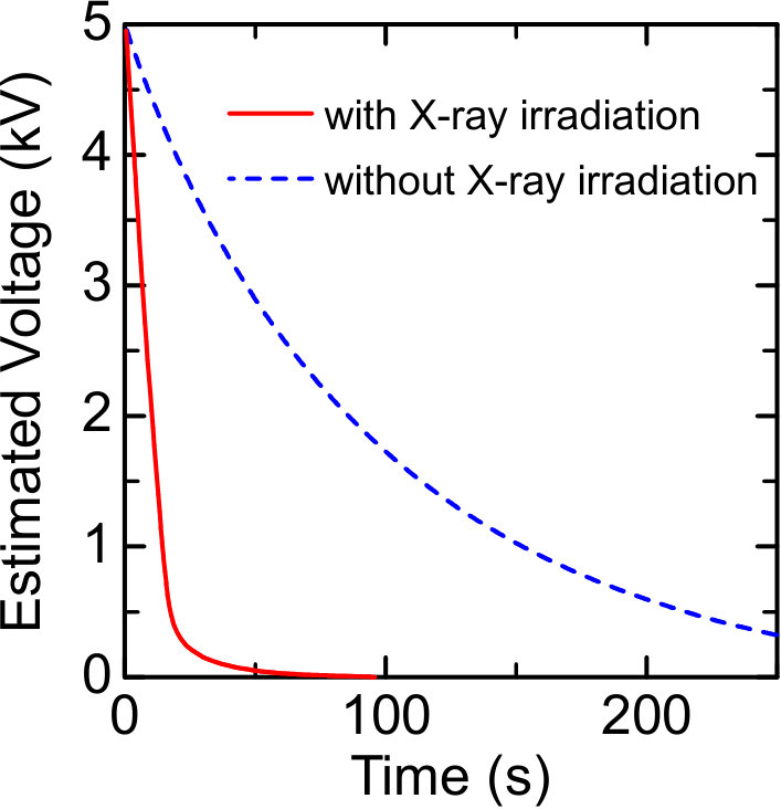 Figure 9
Peer Reviews
No public reviews on file for this paper yet. If you reviewed it on a platform where reviews are public (OpenReview, ICLR, NeurIPS, ICML), you can paste yours below so the community can read it here.
Videos
No videos yet. Explain this paper in a talk, walkthrough, or lecture? Add one.
Characterization of X-ray charge neutralizer using carbon-nanotube field emitter
Shuhei Okawaki
Satoshi Abo
Fujio Wakaya
Corresponding author: [email protected]
Hayato Yamashita
Masayuki Abe
Mikio Takai
Graduate School of Engineering Science, Osaka University, Toyonaka, Osaka 560-8531 Japan
(Dec. 9, 2015 submitted to Jpn. J. Appl. Phys; revised on March 31, 2016)
Abstract
An X-ray charge neutralizer using a screen-printed carbon-nanotube field emitter is demonstrated to show the possibility of a large-area flat-panel charge neutralizer, although the device dimensions in the present work are not very large. The X-ray yields and spectra are characterized to estimate the ion generation rate as one of the figures of merit of neutralizers. Charge neutralization characteristics are measured and show good performance.
Journal reference: Jpn. J. Appl. Phys. 55, 06GF10 (2016) DOI: 10.7567/JJAP.55.06GF10
I Introduction
It is widely known that static electricity causes troubles not only in high-tech industries but also in many fields including the manufacture of plastic, rubber, powder, and paper, and industries of textile, spinning, and printing, meaning that the management of static electricity has been important in many industries for a long time.Noll1995 ; Murata2004 In the ULSI industry, the device dimensions become continuously smallITRS2013 , leading to a more fragile device against static electricity. In the industry of flat-panel displays, the screen size and pixel dimension become continuously large and small, respectively, meaning that the product becomes more sensitive to particle contaminations caused by static electricity. These outstanding trends in high-tech industries suggest that the management of static electricity becomes more critical presently.
Although material modification by antistatic additive doping or surface coating is effective for overcoming static electricity problemsNoll1995 , such a technique cannot always be adopted because, especially for electronic devices, an insulating material is necessary in many cases for realizing device functions. Charge neutralizers using air molecules ionized by corona discharge or soft X-ray irradiation are, therefore, often used for solving static electricity problems. Noll1995 ; Murata2004 ; Choi2004 ; Choi2005 ; Inaba1994 ; Inaba1996 ; Kawai2006
Corona-discharge-type charge neutralizers have the following disadvantages, although they are widely used:Murata2004 (1) the charge balance of ionized air is not good, (2) the discharge process generates particles and causes contamination problems, (3) the density of ionized air is low on the target material surface, although it is high around the discharge electrodes, (4) the discharge process generates electromagnetic noise that may cause troubles in the target devices to be neutralized. The X-ray charge neutralizer has advantages concerning all the above problems. Particularly when the X-ray source is shaped to a large-area flat panel, it should be useful for present large-area flat-panel devices because of the uniform ion density over a large area.
A carbon nanotube (CNT) is one of the promising materials for electron field emitters owing to its high aspect ratio, high current tolerance, high mechanical strength, and high chemical stability.Iijima1991 ; DeHeer1995a ; Collins1996 . Many applications using CNTs as field emitters, such as a field emission display,Wang2001 ; Choi2001 a backlight unit for a liquid crystal display,Kim2005 ; Kim2009 and an X-ray source,Sugie2001 ; Jeong2013 ; Manabe2013 are reported. A screen-printed CNT mat with appropriate post surface treatments is one of the best candidates for realizing a large-area field emitterZhao2002 ; Zhao2003 ; Zhao2004 ; Sawada2003 ; Kanazawa2004 ; Was2005 ; Ohsumi2007 ; Oki2009 ; Takikawa2010 ; Manabe2012 ; Nitta2012 and can be applied to a large-area X-ray sourceManabe2013 ; Okawaki2015 . Although the X-ray generated at the large-area source may not be very suitable for high-resolution X-ray imaging, it should be useful for realizing a large-area X-ray charge neutralizer for large-area flat-panel devices.
In this study, an X-ray charge neutralizer using a screen-printed CNT cathode is demonstrated. Characterization results show good performance for a charge neutralizer.
II Experimental methods
To apply electron field emitters to an X-ray source, a three-terminal configuration with emitters, gate electrodes, and an anode is necessary; such a configuration enables us to control separately the anode current from the anode voltage, leading to the separate control of the X-ray intensity and X-ray energy. An in-plane side-gate structure is adopted in the present work because it is easily applied to a large-area flat-panel emitter. The fabrication process for the emitter, which was already reported,Manabe2012 ; Nitta2012 ; Okawaki2015 is summarized as below. Indium-tin-oxide (ITO) electrodes of mm2, some of which were used as side-gate electrodes and others as back electrodes for CNT cathodes, were deposited on a glass substrate. A CNT paste was screen-printed on a part of the ITO electrodes with an area of mm2. The gap between the edges of the CNT cathode and side-gate electrode is 100 m. The schematic top view of the cathode is shown in Fig. 1.
The effective area of the cathode, which is mm2, is not very large but it can easily be enlarged because screen printing can easily be applied to a large-area process. The tape-peeling surface treatment was performed to improve the electron emission property.Oki2009 ; Takikawa2010
The experimental setup used to generate and detect X-rays is schematically shown in Fig. 2.
In a vacuum of Pa, a 10-m-thick Cu thin film, placed 8 cm away from the emitter, was irradiated by field-emitted electrons from the CNT cathode typically at 10 keV to generate X-rays. To characterize the X-ray spectrum and yield in vacuum, the X-ray detector was set 4 cm away from the Cu film as shown in Fig. 2(a). To characterize X-rays in air, a 250-m-thick Be window was used and the X-ray detector was set in air 5 cm away from the Be window shown in Fig. 2(b). The X-ray detection system used is Amptek XR-100CR/PX4 with a detector area of 13 mm2.
Ion current was measured in air by a metal plate of 40 40 mm2, placed 5 cm away from the Be window instead of the X-ray detector shown in Fig. 2(b). The bias voltage of the plate was kept constant at kV during the measurement. This is not exactly the same as the real neutralization situation, because the voltage of the object material decreases during the real neutralization process. Such a technique, however, is often used for characterizing charge neutralizers.Murata2004 Charge neutralization performance as a function of time was characterized by using the charged plate monitor shown schematically in Fig. 3 placed in air 5 cm away from the Be window.
The area and capacitance of the charged plate monitor are 25 25 mm2 and 25 pF, respectively. The current defined in Fig. 3 was measured as a function of time , since the high-voltage source was disconnected from the circuit. The electric potential of the charged plate, , can be estimated as
[TABLE]
with kV and pF. The direct measurement of is difficult because the ion current and are typically A at the electric potential of V as discussed in the following section, which means that a voltmeter input impedance of more than is necessary. This is the reason why the estimation using Eq. (1) is adopted in this work.
III Results and discussion
The anode current of the CNT cathode with side-gate electrodes was controlled by the side-gate voltage and reached the highest value of 300 A. The detailed field-emission properties were similar to those observed in the previous workOkawaki2015 .
Figure 4 shows the X-ray spectra obtained in vacuum,
the setup for which is shown in Fig. 2(a). The anode current during the measurement was reduced and kept at 1 nA, although it can be increased up to 300 A as described previously, because the X-ray spectrum cannot be measured if it is very strong. The characteristic X-ray peaks of Cu were observed when the anode voltage was 10 kV. For all anode voltages, the maximum energy of the bremsstrahlung X-ray corresponded to the anode voltage as expected.
The X-ray spectra obtained in air are shown in Fig. 5.
When the spectrum was measured in air, the X-ray was absorbed by air and its intensity decreased. The anode current was, therefore, increased to 400 nA, while the other parameters were maintained the same as in the in-vacuum measurement shown in Fig. 4. The maximum energies of the bremsstrahlung X-rays with anode voltages of 8 and 10 kV exceed the corresponding anode voltages not as expected. This is due to the double or multiple counting of photons during the time constant of the detection system.
For the charge neutralizer, the ion generation rate is one of the important figures of merit, which can be estimated as
[TABLE]
where and are the air temperature and pressure, respectively, is the area of the X-ray detector, is the measurement time for obtaining the spectrum, is the X-ray energy of the th channel of the detector, is the average ionization energy of air, is the X-ray yield, is the X-ray absorption coefficient of air, is the mass density of air. Figure 6 shows the ion generation rate estimated from the spectrum shown in Fig. 5 using Eq. (2) with 13 mm2, s, 34 eV, Iida2005 ; Macheret2002 from the database, Hubbell2004 and g/cm3 at 760 Torr and 20 .Rikanempyou1990
The maximum ion generation rate in Fig. 6 is cm*-3s-1*, corresponding to the ion concentration of cm*-3*.Inaba1996 It is reportedInaba1996 that cm*-3* or cm*-3s-1* is enough for a charge neutralizer. The maximum estimated in the present work is two orders of magnitude lower than this value. The ion generation rate can, however, be increased by increasing the anode current, which was intendedly reduced from 300 A to 400 nA in order to obtain the X-ray spectrum shown in Fig. 5. Assuming that is proportional to the anode current, we can expect to be 750 times larger than those in the present work with an anode current of 300 A, the upper limit of the emitter used in the present work. This means that the charge neutralization performance of the present device is fairly good.
The ion currents observed in air by using the metal plate biased at kV are shown in Fig. 7 as a function of the anode current.
The ion current was roughly proportional to the anode current as expected. The absolute value of ion current with positive bias should be similar because it is considered that the ion balance of the X-ray charge neutralizer is better than that of the corona-discharge-type neutralizerMurata2004 , although the measurement with positive bias was not performed owing to the voltage source restriction.
The measured current to the ground plate , defined in Fig. 3, is shown in Fig. 8.
For this measurement, the anode current was increased and fixed to 300 A to obtain the highest neutralization performance. When the current shown in this figure is used with Eq. (1), after a sufficiently long time. This is probably due to the unreliable value of the capacitance . If is assumed to be % larger than 25 pF, after a sufficiently long time. The following normalization was, therefore, used instead of Eq. (1) to avoid the problem:
[TABLE]
The resulting estimated electronic potentials at the charged plate with and without X-ray irradiation are shown in Fig. 9.
The decay observed without X-ray irradiation should be due to the natural neutralization of the charged plate interacting with the surrounding air. If the decay time is defined as the time at which the voltage becomes of the initial value, it is estimated to be 17.5 and 215 s with and without X-ray irradiation, respectively. The decay time of 17.5 s with X-ray irradiation is not very good compared with the referenceInaba1996 , but can be improved by increasing the X-ray intensity. The X-ray intensity can be increased by decreasing the distances between the Cu target and the Be window and between the Be window and the object material to be neutralized, which are 13 and 5 cm, respectively, in the present work for the preliminary demonstration.
IV Conclusions
An X-ray charge neutralizer was demonstrated by using a screen-printed CNT field emitter. The effective area of the emitter is mm2. This is not very large and is almost a point source because the distances in the present work between the emitter and the Cu target, between the Cu target and the Be window, and between the Be window and the object material to be neutralized are 8, 13, and 5 cm, respectively. To realize a large-area flat-panel source is not difficult because screen printing can be easily applied to a large-area process. Charge neutralization characteristics were measured and showed good performance even under such an almost point-source condition, suggesting that the performance is much improved when a vacuum-sealed large-area flat-panel charge neutralizer is realized using the screen-printed CNT field emitter.
Acknowledgements.
This work was partially supported by JSPS KAKENHI Grant Number 23360022.
The reference list from the paper itself. Each links out to its DOI / PubMed record.
- 1(1) C. G. Noll, in Handbook of Electrostatic Processes , ed. J.-S. Chang, A. J. Kelly, and J. M. Crowley, (Marcel Dekker, New York, 1995) Chap. 33.
- 2(2) Seidenki Joden no Sochi to Gijutsu (Ionizer and Tehnique of Charge Eliminating), ed. Y. Murata (CMC, Tokyo, 2004) [in Japanerse].
- 3(3) International Technology Roadmap for Semiconductors 2013 Edition Executive Summary (2013) [ [ [ http://www.itrs.net ] ] ] .
- 4(4) K.-S. Choi, T. Fujiki, and Y. Murata, Jpn. J. Appl. Phys. 43 , 7693 (2004).
- 5(5) K.-S. Choi, S. Nakamura, and Y. Murata, Jpn. J. Appl. Phys. 44 , 3248 (2005).
- 6(6) H. Inaba, T. Ohmi, T. Yoshida, and T. Okada, J. Electrostat. 33 , 15 (1994).
- 7(7) H. Inaba, T. Ohmi, T. Yoshida, and T. Okada, IEICE Trans. Electron. E 79-C , 328 (1996).
- 8(8) J. Kawai, H. Ishii, and Y. Hosokawa, Int. Symp. Discharges and Electrical Insulation in Vacuum , 2006, Vol. 2, p. 628.