Multi-scale approach to first-principles electron transport beyond 100 nm
Gaetano Calogero, Nick R. Papior, Mohammad Koleini, Matthew, Helmi Leth Larsen, Mads Brandbyge

TL;DR
This paper introduces a multi-scale computational method combining DFT and tight-binding models to simulate electron transport in large 2D devices over 100 nm, capturing atomistic details and complex device features.
Contribution
The paper presents a novel multi-scale approach that integrates DFT and tight-binding models for large-scale 2D electron transport simulations beyond 100 nm.
Findings
Successfully applied to pristine, defected, and nanoporous graphene devices
Enabled atomistic-level current propagation analysis in large devices
Addressed practical implementation challenges of multi-scale modeling
Abstract
Multi-scale computational approaches are important for studies of novel, low-dimensional electronic devices since they are able to capture the different length-scales involved in the device operation, and at the same time describe critical parts such as surfaces, defects, interfaces, gates, and applied bias, on a atomistic, quantum-chemical level. Here we present a multi-scale method which enables calculations of electronic currents in two-dimensional devices larger than 100 nm, where multiple perturbed regions described by density functional theory (DFT) are embedded into an extended unperturbed region described by a DFT-parametrized tight-binding model. We explain the details of the method, provide examples, and point out the main challenges regarding its practical implementation. Finally we apply it to study current propagation in pristine, defected and nanoporous graphene…
Click any figure to enlarge with its caption.
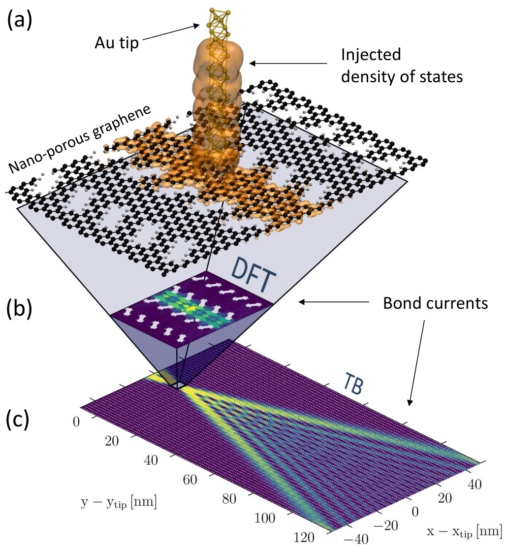 Figure 1
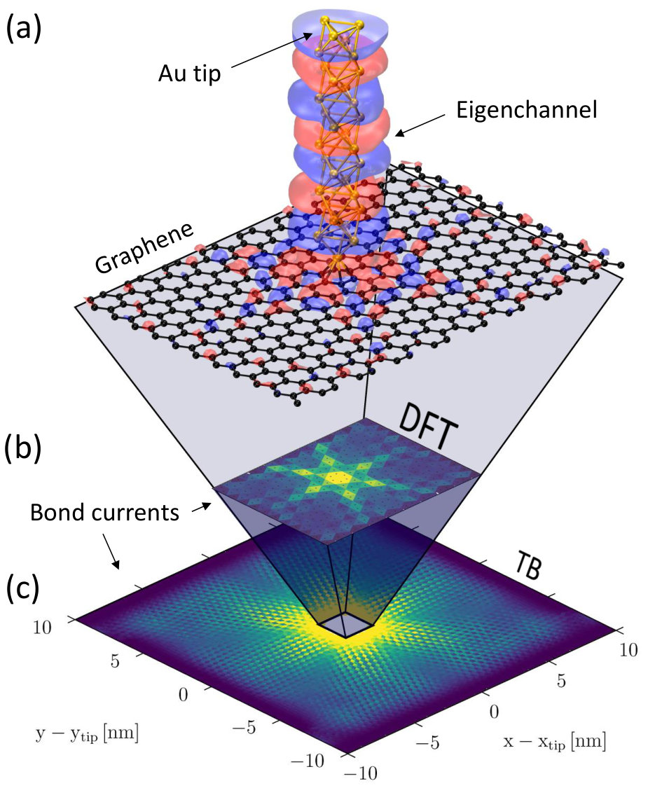 Figure 2
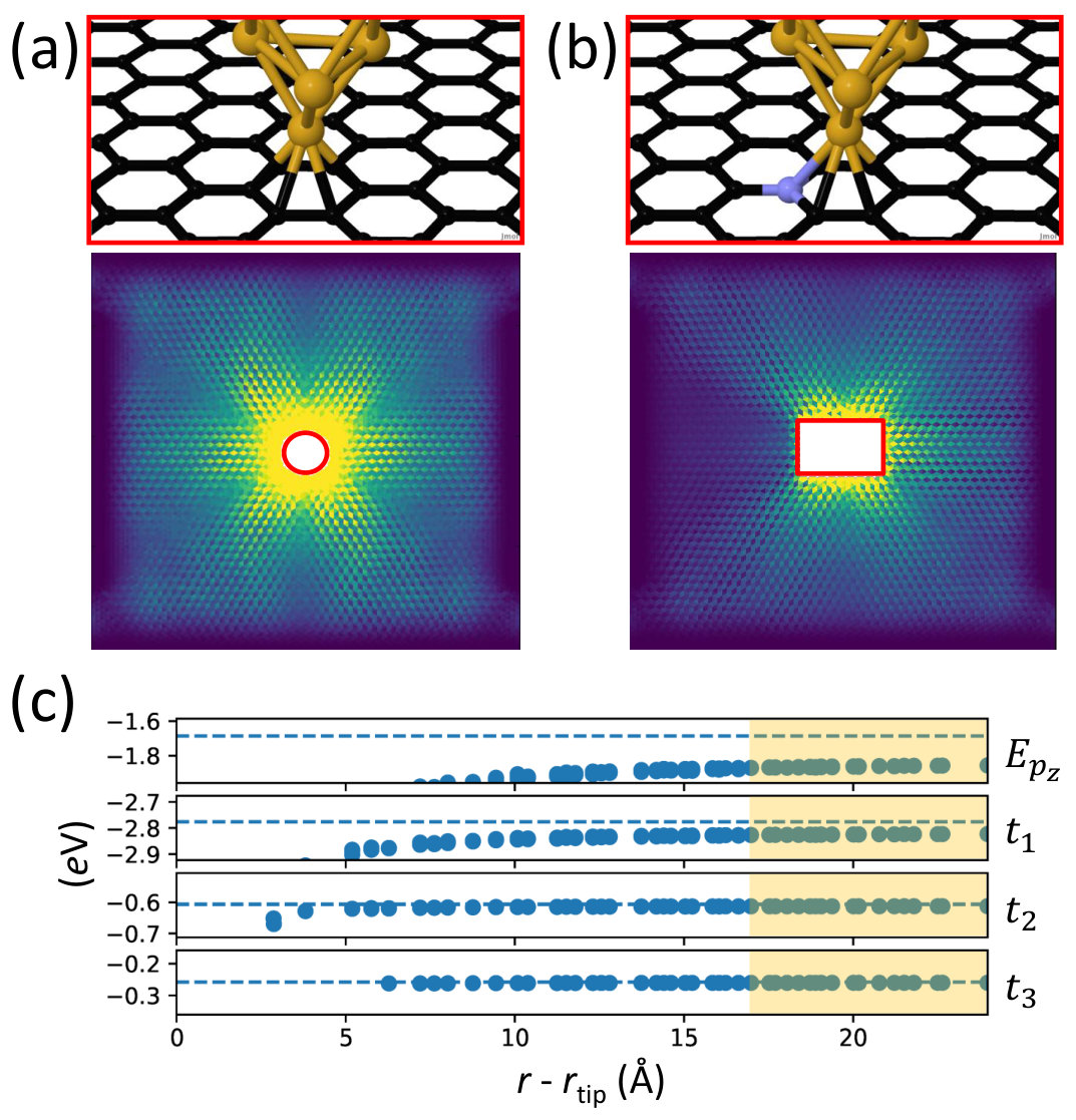 Figure 3
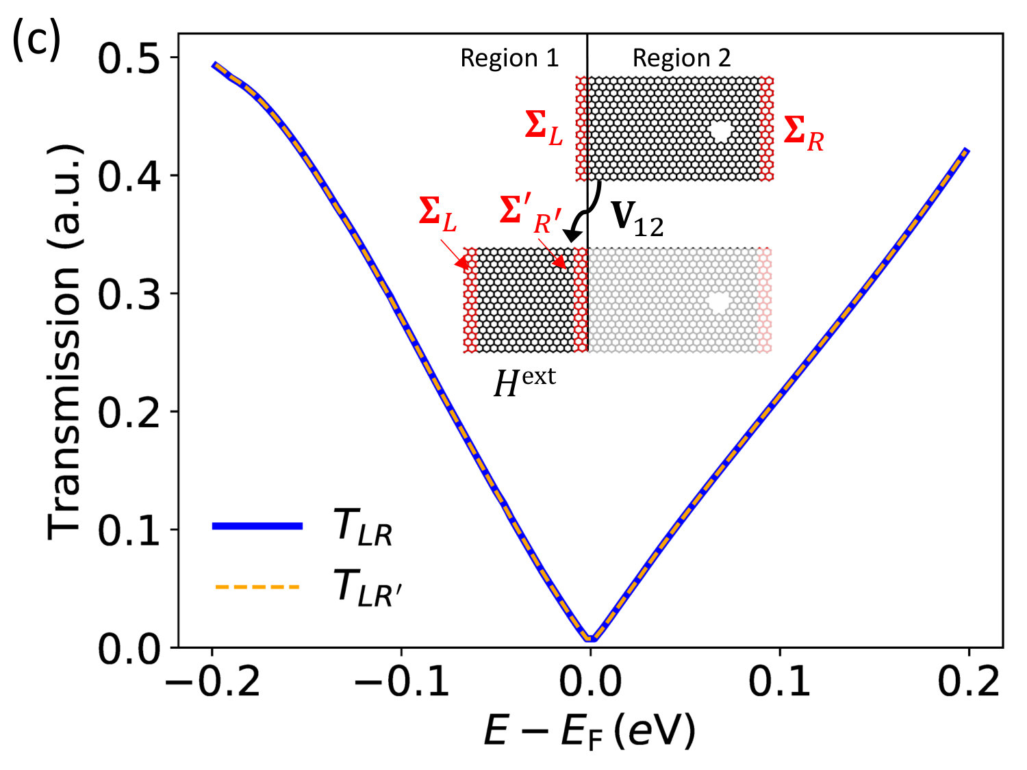 Figure 4
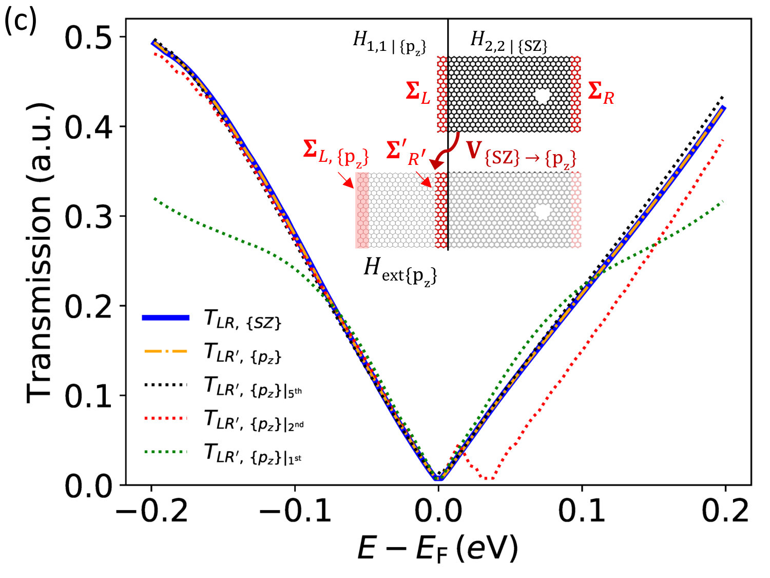 Figure 5
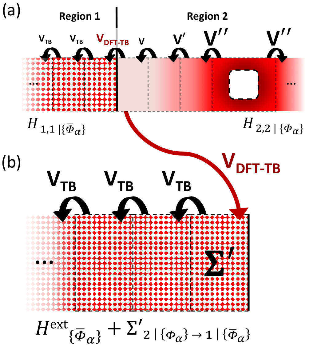 Figure 6
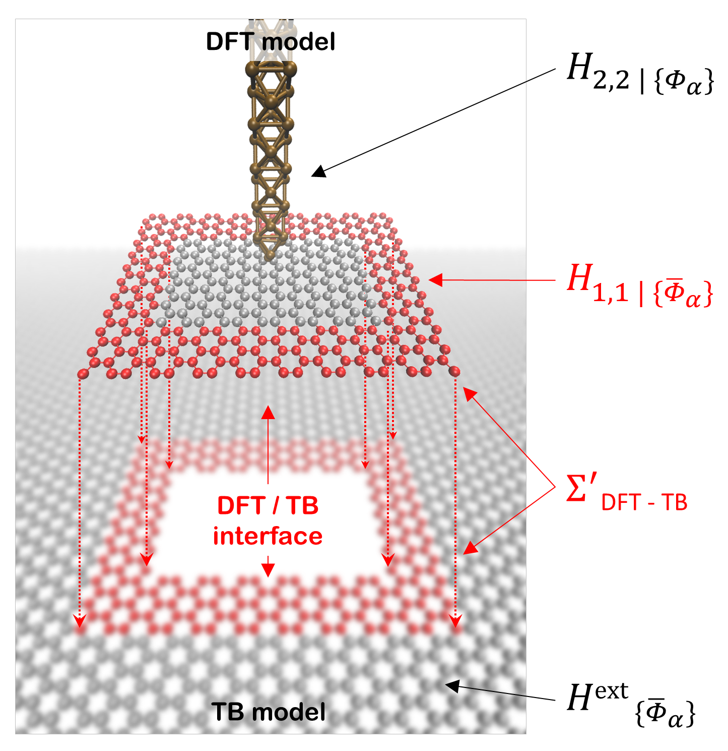 Figure 7
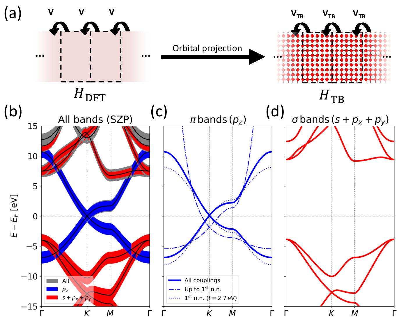 Figure 8
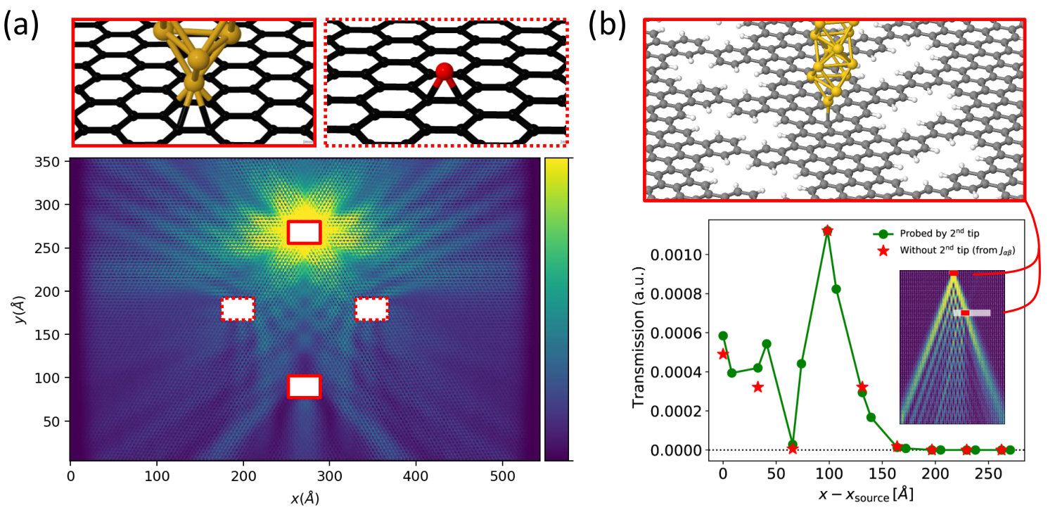 Figure 9
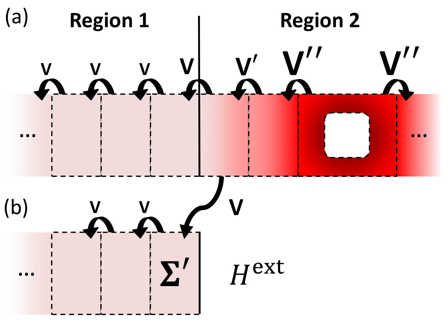 Figure 10
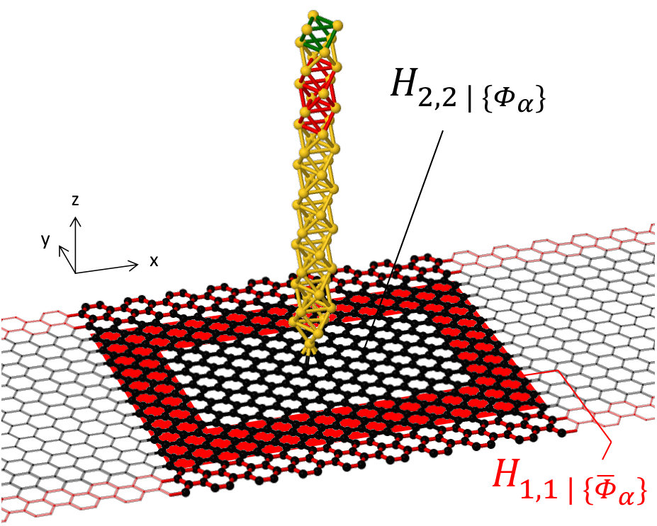 Figure 11
Peer Reviews
No public reviews on file for this paper yet. If you reviewed it on a platform where reviews are public (OpenReview, ICLR, NeurIPS, ICML), you can paste yours below so the community can read it here.
Videos
No videos yet. Explain this paper in a talk, walkthrough, or lecture? Add one.
Multi-scale approach to first-principles electron transport beyond 100 nm
Gaetano Calogero
Dept. of Physics, Technical University of Denmark, DK-2800 Kongens Lyngby, Denmark
Center for Nanostructured Graphene (CNG), DK-2800 Kongens Lyngby, Denmark
Nick R. Papior
Computing Center, Technical University of Denmark, DK-2800 Kongens Lyngby, Denmark
Center for Nanostructured Graphene (CNG), DK-2800 Kongens Lyngby, Denmark
Mohammad Koleini
Dept. of Physics, Technical University of Denmark, DK-2800 Kongens Lyngby, Denmark
Center for Nanostructured Graphene (CNG), DK-2800 Kongens Lyngby, Denmark
Matthew Helmi Leth Larsen
Dept. of Physics, Technical University of Denmark, DK-2800 Kongens Lyngby, Denmark
Mads Brandbyge
Dept. of Physics, Technical University of Denmark, DK-2800 Kongens Lyngby, Denmark
Center for Nanostructured Graphene (CNG), DK-2800 Kongens Lyngby, Denmark
[email protected], [email protected]
Abstract
Multi-scale computational approaches are important for studies of novel, low-dimensional electronic devices since they are able to capture the different length-scales involved in the device operation, and at the same time describe critical parts such as surfaces, defects, interfaces, gates, and applied bias, on a atomistic, quantum-chemical level. Here we present a multi-scale method which enables calculations of electronic currents in two-dimensional devices larger than 100 nm2, where multiple perturbed regions described by density functional theory (DFT) are embedded into an extended unperturbed region described by a DFT-parametrized tight-binding model. We explain the details of the method, provide examples, and point out the main challenges regarding its practical implementation. Finally we apply it to study current propagation in pristine, defected and nanoporous graphene devices, injected by chemically accurate contacts simulating scanning tunneling microscopy probes.
I Introduction
Developing high-performance computational strategies to simulate electronic devices is a fundamental asset for prototype design and research planning in basically any technological context.Hofer2018 ; Marzari2016 ; Thijssen2007 Being able to model nanometer-scale devices with atomic resolution has become particularly crucial for e.g. novel low-dimensional materials, molecular junctions, or, generally, ballistic quantum systems which have appeared on the electronics horizon in the last decades.Aprojanz2018 ; Shulaker2013 ; Ferrari2015 ; Novoselov2016 ; Geim2013 ; Martinez-Blanco2015 ; Moreno2018 ; Jia2016 ; Cao2018 Quantum-chemical details are often critical for describing local electronic structure, chemical contacts (e.g. electrodesKretz2018 ; Palacios2008 ) and electrostatics in realistic nano-electronic devices. This is especially clear in a context of one-atom-thick two-dimensional (2D) devices,Fiori2014 ; Novoselov2016 ; Iannaccone2018 where details on the atomic scale govern the electronic behavior.Schedin2007 ; Wehling2008 ; Chang2012 ; Caridad2018 ; talbotNPG These details can be accessed using various ab-initio methods,Szabo1989 ; Levine2014 ; Thijssen2007 in particular density functional theory (DFT),Kohn1965 ; Hohenberg1964 which can be used to simulate up to thousands of atoms.Goedecker1999 ; Mohr2015 ; Lin2014 This is typically enough to simulate isolated portions of a realistic device, such as bulk regions, interfaces or locally perturbed areas, but it is not suitable to simulate all the different length-scales involved in the operation of realistic devices.
A promising solution which is rapidly growing along many lines of research is to perform hybrid multi-scale simulations.Hofer2018 ; Hofer2015 ; Troisi2006 ; Kubar2010 ; Zhang2018 ; Shen2016 ; Fiori2013 ; AufDerMaur2011 ; Fediai2016 ; Fediai2016b In this context an interesting approach is to treat crucial parts of a relatively large device using full quantum-chemical detail, while reducing the number of degrees of freedom to the bare essentials elsewhere.Hofer2018 ; Hofer2015 ; Troisi2006 ; Kubar2010 ; Zhang2018 ; Shen2016 ; Ng2008 ; Rapacioli2011 A very popular example, coming from a biomolecular context, is the quantum mechanics/molecular mechanics (QM/MM) technique,Warshel1976 which has also been generalized to study solid-state surfaces and interfaces.Hofer2015 The key problem of multi-scale approaches is to partition the system into a number of subregions and, most importantly, to ensure a smooth, physically sound, transition among them.Hofer2018
Electronic structure methods employing linear combinations of atomic orbitals (LCAO) provides an intuitive route for elaborating multi-scale approaches analogous to QM/MM for simulating electron transport, as the accuracy and scalability of LCAO-based approaches can be “tuned” via clever approximations of the Hamiltonian. One common case is the Density Functional Tight-Binding (DFTB), which is based on a Taylor series expansion of the Kohn-Sham DFT total energy.Elstner1998 ; Elstner2014 Once a reliable element or compound-specific parametrization has been obtained, either comparing to experiments or higher-level ab-initio calculations, DFTB can be two to three orders of magnitude faster than DFT,Gaus2013 overall enabling simulations with several thousand atoms without need for any massive parallelization.Elstner2014 Another useful approximation is the Wannier Tight-Binding (WTB), where maximally localized Wannier functions (MLWF) are constructed ad-hoc to reproduce electronic bands from plane-wave DFT within optimized energy windows.Marzari1997 ; Marzari2012 ; Bruzzone2014 ; Marin2018 ; Lv2015 ; Pizzi2016 Once a system-specific parameterization is found, and good initial trial orbitals are defined,Gresch2018 one can use WTB to access samples containing hundreds of thousands of atoms.Rudenko2015 The latter two tight-binding (TB) like approximations can be ultimately simplified by reducing the number of orbitals per atom to a minimum, and limiting the interaction range to only a few nearest neighbors in the lattice, fitting parameters by hand to experiments or ab-initio calculations.Martin2004 ; Ashcroft ; Liu2015 ; Beconcini2016 ; Calogero2018 Multi-scale approaches for electron transport based on these models have been proposed and include combinations of Classical Molecular Dynamics (CMD) and DFT with Langevin Dynamics,Troisi2006 combinations of CMD, DFTB, and wave function propagation,Kubar2010 or combinations of TB models with patched Green’s function techniques.Settnes2015
In this article we present a multi-scale scheme based on seamless integration of a number of perturbed regions described by DFT and an unperturbed extended region represented by a simpler representative LCAO model, namely TB. We parametrize the TB Hamiltonian directly from DFT, such that the resulting multi-scale model is defined without any fitting parameter or by hand adjustments. The obtained models can be combined with the non-equilibrium Green’s function (NEGF) formalismTaGuWa2001 ; Brandbyge2002 ; Datta2000 ; Papior2017 to enable current simulations of over large devices with local quantum-chemical detail. The manuscript is divided into two main sections. In the first section we develop the general formalism, didactically providing concrete examples based on simple graphene two-electrode devices. In the second section we apply the multi-scale approach for imaging real-space “far-field” currents (i.e. far from the source) in pristine, defected and nanoporous graphene, injected by chemically accurate contacts simulating Scanning Tunnel Microscopy (STM) probes.
II Method
II.1 TB models from orbital-projected DFT
Our starting point is a pristine structure of a periodically repeated unit cell, illustrated in Fig. 1, and a DFT Hamiltonian describing this system with a localized basis. We will here consider a LCAO basis for the DFT calculation, , but it could equally well be a basis obtained from e.g. maximally localized Wannier states. We will from this construct a smaller TB-like basis, which only describe the bands in a region around the Fermi energy, , set via a projection ,
[TABLE]
In the simplest case, used here, this involves selecting a particular subset of the original DFT basis functions, however one may imagine more involved projections. Our prime example is shown in Fig. 1b, where we consider the bandstructure of graphene obtained with DFT and a LCAO single- plus polarization basis (i.e. a single orbital for each , states and polarization orbitals). A TB-like model can be readily constructed by projecting on to the orbitals of the DFT LCAO Hamiltonian (and overlap), by extracting all rows and columns associated to orbitals. This cheaper model is sufficient to capture the bands of graphene (Fig. 1c). Likewise, the bands further away from the Dirac point energy can be captured using a TB model parametrized from , and DFT orbitals (Fig. 1d). Importantly, as highlighted (dashed lines) in Fig. 1c, a partial -projection where only couplings among nearest neighbors are retained results in significant band-misalignment and rescaling. Analogous but less dramatic deviations are observed when using a standard nearest neighbor model with orthogonal basis and hopping .
II.2 Multi-scale approach
In the following we omit energy and dependence, highlighting it only where necessary.
The multi-scale method presented in this work is based on the Non-Equilibrium Green’s Function (NEGF) transport formalism.TaGuWa2001 ; Brandbyge2002 ; Datta2000 ; Papior2017 In the NEGF framework transmission between any two leads and of a -electrode device with Hamiltonian and overlap is given by
[TABLE]
where the device Green’s function is given by
[TABLE]
and are the so-called self-energies of the semi-infinite electrodes.
It is the self-energies that will play a pivoting role in connecting TB and DFT models. The self-energy is nothing but the effect of degrees of freedom not accounted explicitly for in the equation but have been eliminated as can be done for variables in linear equations. The self-energies can represent the semi-infinite electrodes as well as a finite number of degrees of freedom in the case of a finite region. In the following we show that it is in practice possible to locally replace small perturbed regions of a large TB device with DFT-precision models by simply including one or more “special” self-energies in the sum of Eq. (4).
II.2.1 Self-energy for a partitioned system
To understand the construction of these special self-energies it is instructive to recall the definition of self-energy connecting two subregions of a generic binary system. We do this by simply generalizing the derivation of self-energy for a simple system divided into two parts.PapiorThesis
Let us consider the system in Fig. 2a, with Hamiltonian , and overlap (we use an orthogonal basis without loss of generality),
[TABLE]
Here we have explicitly indicated with the coupling of region 1 () to the neighboring region 2 (). In the following we are only interested in the Green’s function in region , and thus a derivation of this matrix is required. The full Green’s function is
[TABLE]
with and . By using the Dyson equation
[TABLE]
we can express the Green’s function in only one region
[TABLE]
and thus
[TABLE]
Here the term
[TABLE]
is the self-energy describing how region 1 is perturbed by the coupling to the degrees of freedom in region 2. In case of a non-orthogonal basis set () Eq. (14) simply becomes
[TABLE]
The real part of the self-energy is an energy renomarlization/shift, while the, possibly finite, imaginary part corresponds to a finite life-time or broadening of the energy levels in region 1. Additionally the self-energy is independent of and may thus be used in any other system so long as the coupling matrix is unchanged, i.e. .
In Fig. 2a, we see the above exemplified using an extended system with a hole perturbing the local potential (dark colors). After two layers the perturbation goes to zero and the coupling between neighbouring cells turns to the bulk value(). At this point one can calculate for region 2, insert it into an external pristine system (equal to region 1 in Fig. 2b) and, in turn, reproduce the correct Green’s function in region 1, as though the new system was connected with the hole.
II.2.2 Example: graphene device with DFT-DFT connection
In the following we illustrate with a concrete example where the two models, connected by , are constructed using the same method (here DFT with a SZ basis set, i.e. 4 orbitals per C atom), then effects of the perturbation can be propagated from one model to the other with 100% accuracy. Consider the basic DFT two-electrode graphene device illustrated in Fig. 2c (upper inset). This has periodic boundary conditions along , semi-infinite electrodes and along and a hole in the scattering region. Total transmission across the device can easily be computed by using Eq. (2) and is plotted in Fig. 2c. One can choose to split this device into two sections, a bulk part (region 1) and a perturbed region 2 (hole). Since the potential of the hole is fully screened in region 1, we have that the coupling between equals the bulk coupling, . Hence one can construct the self-energy which contains the effects of region 2 propagated into region 1 using Eq. (14). This can then be incorporated as a new electrode on the right side of an external DFT device which has no holes in the scattering region (lower inset) and verify that for all within the numerical accuracy.
II.3 Self-energy for DFT-TB connections
We now turn to the more interesting situation where the perturbation and the external unperturbed system hosting its self-energy are modelled using different basis sets, e.g. DFT and TB. We have already anticipated with the example in Fig. 1 that the electronic structure of a DFT system within a particular energy window often can be reproduced by a small TB model obtained as a projection of the DFT Hamiltonian. The drastically reduced number of orbitals in a TB model makes it potentially very convenient for generating unperturbed external host systems with large dimensions, normally inaccessible by DFT calculations. By generalizing the definition of the self-energy, , it becomes possible to incorporate DFT-precision perturbations in TB models. However determining a self-energy for a DFT-TB connection is not as trivial as for the basic DFT-DFT connection described in the previous section.
Consider now the system as shown in Fig. 3a. Instead of having both regions (1 and 2) using the same basis set, we change the basis set in region 1 to be a TB parameterized basis set, , as discussed in Fig. 1. Here the approximation lies in . By the same arguments outlined in the theory section, we create the subset of such that the rows correspond to the full basis set and the columns correspond to the projection orbitals . Using in Eq. (14) results in a projection of the self-energy onto the parameterized orbitals. Importantly, the fact that some elements of the original DFT coupling, , are now missing in inevitably leads to some scattering at the DFT-TB boundary.
II.3.1 Example: graphene device with DFT-TB connection
We have demonstrated that a TB model fully parametrized from DFT can reproduce the bands of graphene with only minimal deviations (Fig. 1c). As a result DFT results can be reproduced, within accuracy, using the multi-scale DFT-TB approach. Let us consider again the graphene device with a hole, as shown in Fig. 3a. The only difference between DFT-DFT and DFT-TB is that here , in Eq. (14), is chosen such that the columns of project onto the parameterized orbitals. This yields a self-energy only existing on the orbitals in the TB model. However, one may additionally play with the number of neighbors each atom connects with, e.g. 1, 2, 3 or all neighbors (with “all” defined by the DFT basis).
In Fig. 3c the transmission for the hole system is shown at four levels of precision compared to the full DFT calculation. We find that if the TB parametrization contains only DFT couplings among nearest neighbors then the transmission spectrum undergoes significant scattering 0.1 eV away from the Dirac point. When the range of interaction is extended to 2, 3 or 4 neighbors the transmission spectrum becomes comparable to DFT in a wider energy range, except for a shift at positive energies. As soon as couplings among 5 nearest neighbors are included we obtain an almost perfect agreement with DFT.
II.4 Self-energy of isolated perturbations
In all the examples considered so far periodic boundary conditions was employed in the DFT calculations from which the connecting self-energy was constructed. This means that the perturbation, e.g. the hole, is periodically repeated along the transverse direction . However, if the potential is screened to the bulk value one may replace the surrounding periodic images by other environments with the same potential and Hamiltonian. In this way one may effectively change the boundary conditions.
The origin of this versatility lies in the fact that the two regions in which the perturbed DFT model is divided can have arbitrary size, shape and periodicity. For example, with reference to Fig. 3, one could choose to define the pristine DFT region 1 as the outermost frame-shaped area of the cell surrounding the perturbation, while treating all the orbitals enclosed by it as region 2. The same formalism discussed above can be readily applied to this case, with the only difference that periodic boundary conditions are removed from the DFT Hamiltonian before constructing the self-energy .
An example is illustrated in Fig. 4. The top geometry is the DFT region which is used in calculating . The bottom geometry is the TB parameterization and the red atoms indicate the overlay region where the self-energy is transferred from region 1 (DFT) to region 2 (TB). We point out that this particular approach provides the basis for “modular” multi-scale simulations, where multiple DFT-precision perturbations, modules, are incorporated into the same large TB device. We will present concrete applications of this in the second part of the work.
II.5 Challenges and implementation
Despite reflecting a conceptually simple theory, the protocol to embed DFT-precision perturbations locally into an unperturbed TB region parametrized from DFT implies a number of critical issues when it comes to its practical implementation. Let us briefly go through the procedure to include non-periodic DFT perturbations into large TB models step-by-step:
Generate a DFT model of the perturbation. This can be represented by either a bulk (periodic) or device (semi-infinite electrodes) setup and must be large enough to ensure the potential turns constant in its outermost areas; 2. 2.
Define two regions in the DFT system, one containing all orbitals involved in the perturbation and the other involving the projection orbitals. The latter needs to be as far as possible from the perturbation so as to ensure ; 3. 3.
Represent the DFT Hamiltonian and overlap in real-space (without periodic boundary conditions); 4. 4.
Compute the self-energy using equation Eq. (14); 5. 5.
Generate a DFT model of the same system, but without the perturbation; 6. 6.
Construct a large TB model using parameters from the projection of the unperturbed DFT calculation. 7. 7.
Incorporate the self-energy locally into the TB model using Eq. (4).
To begin with, most of the described steps require flexible manipulation of the DFT Hamiltonian and overlap matrices. Extraction of selected on- and off-diagonal elements exclusively associated to a subset of orbitals is crucial to compute , extract or to create TB models parametrized from DFT. Secondly, to ensure the correct couplings at the DFT-TB interface when incorporating into the TB model, it is important that region/atoms selected to host in the large TB geometry have a one-to-one correspondence with those in region 1 of the DFT geometry. User-friendly tools to access and compare lattice coordinates of the various involved geometries are therefore highly desirable.
Furthermore, the self-energy, , needs to be stored into external files with general and compact format, readily accessible for usage in NEGF calculations. Being able to flexibly input/output self-energies into external host models is especially crucial to carry out multi-scale calculations where several DFT-precision regions are accounted for in the same large TB device.
Overall, the computation of through Eq. (14) and NEGF transmissions needs to be optimized both time and memory-wise, so as to efficiently handle dense DFT matrices and large sparse TB ones, as well as calculation of the self-energy for a fine grid and several energy values.
Computational tools
We tackle all the issues described in the previous section with open-source tools TBtrans and sisl.Papior2017 ; Papior2017a TBtrans is distributed with the Siesta/TranSiesta software package.Soler2002 ; Papior2017 TranSiesta enables high-performance DFT+NEGF self-consistent calculations of large, multi-terminal systems under various electrostatic conditions (e.g. gating.Papior2015 ) TBtrans is a post-processing NEGF code which provides a flexible interface to DFT or TB Hamiltonians and enables large-scale calculations of spectral physical quantities, interpolated - curves and/or orbital/bond-currents for systems easily exceeding millions of orbitals on few-core machines. sisl is a Python package used to create and/or manipulate DFT and TB models for arbitrary geometries, with any number of orbitals and any periodicity.Calogero2018 The device Green’s function in TBtrans is generally implemented as:
[TABLE]
where and are DFT or TB-modeled overlap and Hamiltonian, are the electrodes self-energies and is a user-defined, optional, perturbative term. The flexibility of using sisl and TBtrans is appreciated since no code extension of TBtrans is required as everything being done is added using and terms. Implementation of these two terms in Eq. (16) is done only in Python and is thus much simpler than a full fortran implementation. Secondly, both sisl and TBtrans are scaling easily to millions of orbitals in the TB method.
All of the calculations described in this article have been carried out using a single high-performance computing node with 20 cores (Core Intel Xeon E5-2660v3, 2.6GHz, 128GB RAM), parallelizing TBtrans and either MPI or OMP parallelization. The transmission spectra in Fig. 2 and Fig. 3 were calculated in TBtrans using 100 energy points, 201 k-points in the periodic direction and a total of 540 atoms. The computationally most expensive calculation presented so far, i.e. , that involving a DFT-DFT connection, required 3 hours and 50 minutes to compute/store the connecting self-energy , and 10 minutes (53MB RAM, 113kB disk) to calculate transmission with TBtrans.
III Applications
In the second part of this work we show how the multi-scale approach can be used to study the far-field behavior of electrons injected from atomic-scale contacts into large-scale graphene-based devices.
Being able to interpret and predict the behavior of electrons over large-scale devices is of importance for graphene-based electronics, especially in the growing field of electron optics. Real-space visualization of charge (or spin) transport can be achieved experimentally using various quantum imaging techniques, including probe microscopy,Hiraoka2017 ; Kolmer2017 superconducting interferometryAllen2015 and magnetometry with diamond-NV centers.Casola2018 It has been shown that defects and contacts with tips at the atomic scale yield strong spatial variations of current flow in graphene devices.Bhandari2016 ; Tetienne2017
Modeling realistic atomic-scale contacts to inject currents in graphene devices, while simultaneously accessing current flow far away from them, is a challenge for state-of-the-art atomistic transport calculations. Large graphene devices can be accessed using the TB approximation. Despite allowing for good scalability, in this context the complex chemical nature of defects or tip contacts is often subject to drastic simplifications. For instance a STM probe is usually modeled as a constant, on-site, level broadening () self-energy term in the Green’s function,Aprojanz2018 ; Settnes2014 a localized effective force or electrostatic field,Eder2013 ; Mark2017 or even as a narrow semi-infinite in-plane electrode.Calogero2018 On the other hand, DFT-based models have often demonstrated to successfully corroborate probe microscopy measurements on graphene, even when involving complex tip functionalizations or inelastic effects.Jelinek2017 ; Frederiksen2011 ; Palsgaard2015 ; Heijden2016 This is due to an accurate description of tip structure and orbital symmetries, as well as charge and potential variations in the sampled regions.
The essential need for both scalability and accuracy in this problem calls for the multi-scale approach described above. In the following we will provide a bird’s eye view on carrier injection from point sources into pristine, defected and nano-porous graphene (NPG). Furthermore, In order to further emphasize the versatility of the method, we will show an example where multiple DFT-precision regions from various DFT calculations are included in the same large-scale TB transport calculation.
III.1 Far-field currents in graphene
Here we use the multi-scale approach to predict the far-field behavior of electrons injected by a DFT-precision gold tip into a large-scale TB model of pristine graphene. Using wave-packet dynamics simulations to inject currents from an effective electrostatic field model of STM tip, Mark et al. reported anisotropic electron current in graphene.Mark2012 The authors predicted that a well-defined six-fold asymmetry current pattern occurs when the wave packet is injected in the middle of a hexagon in the graphene lattice.Mark2012 Below we confirm this anisotropic signature by looking at the far-field currents flowing up to 10 nm away from the injection. The system is modeled by TB and is coupled to a small DFT-precision injection region through a self-energy . We will limit our focus to a single representative energy value where this six-fold anisotropy is clearly visible.
We start by setting up a three-electrode DFT model device (see Fig. 5) consisting of a semi-infinite gold tip placed above the center of a graphene hexagon and two semi-infinite graphene electrodes along . The tip structure is chosen so as to ensure a flat local density of states on the tip apex in a wide energy interval, . We optimize the tip apex atom and the nearest C atoms in Siesta until forces are less than , using periodic boundary conditions along and , a -point Monkhorst-Pack grid, the GGA-PBE exchange-correlation functional,Perdew1996 a SZP basis set and an energy cutoff of 300 Ry. The tip is in chemical contact to graphene, therefore we assume van der Waals interactions to be negligible and do not include them in the calculations. We then calculate bond-currents flowing across the three-electrodes device using the tip as a source, using -points to sample the direction in TBtrans. In order to avoid artificial crosstalk with periodic images of the tip when computing the injected bond-currents, we substitute the self-energies for the two graphene electrodes with a new self-energy term in Eq. (4),
[TABLE]
where represents an average over all -points along , i.e. the quantities in the principal unit cell in real-space.Papior2019 In effect, this is equivalent to setting up a new drain electrode in the border region of the cell.
The results for are summarized in Fig. 6. We find that the total transmission from tip to is . This is determined mainly by three transmission eigenchannelsPaulsson2007 . The two with largest contribution (37% and 34% of the total transmission) are mostly delocalized over the whole graphene structure, whereas the third one (contributing with 29%) exhibits a preferential propagation along the six armchair lattice directions departing from the probed graphene hexagon (Fig. 6a). We find that this six-fold anisotropy dominates the bond-current pattern injected by the tip at this energy (Fig. 6b).
Then, using the approach discussed in Fig. 4, we insert the DFT-precision injection region inside a larger TB model parameterized from DFT, using a complex absorbing potentialCalogero2018 ; Xie2014 (CAP) to absorb currents at the cell boundaries. As shown in Fig. 6c we find that the six-fold anisotropic propagation can still be observed far away from the source, although collimation is rapidly lost. As a check we estimate transmission outgoing from the tip by summing over positive bond-currents which cross a circle of radius centered at the tip coordinates. The result, , is only slightly lower than the value obtained by summing bond-currents in the smaller all-DFT system, , regardless the choice of radius .
Importantly, we find that the result does not change if the shape of the DFT region in which is computed is modified from a rectangular to a circular one (Fig. 7a).
Effects of single N dopant on far-field currents
One major advantage of the multi-scale approach is that complex situations, e.g. where different perturbations simultaneously affect the same region, can be described with chemical accuracy. An illustrative example is depicted in Fig. 7b, where the multi-scale method has been used to study how a N substitutional dopant in proximity of the Au tip contact affects the far-field currents. In order to unravel possible effects of spin polarization we carry out this calculations for its two possible spin configurations. We find that in both cases, due to the local doping induced by the N atom, electrons injected by the tip are prevented from propagating towards the N atom (Fig. 7c).
TB parameterization
We point out that, compared to the simple case discussed in Fig. 3, the presence of a metal contact in these systems alters the graphene work-function, and hence its potential and couplings far from the tip. As a result, parameterizing the TB model directly from a DFT calculation of pristine graphene would induce some degree of coupling mismatch at the interface between the two models. The solution we adopt here to ensure constant coupling is to parameterize the TB model from the pristine-like DFT elements associated to the atoms far away from the tip, namely those further than from it (Fig. 7c).
III.2 Far-field currents in nanoporous graphene
The principles behind the multi-scale method are general and not limited to the basic graphene systems presented above. For instance, let us now consider nanoporous graphene (NPG), which is inherently semiconducting and anisotropic.Pedersen2008 In particular we consider the NPG structure shown in Fig. 8a, which has recently been fabricated through bottom-up synthesis with unprecedented sample sizes and quality.Moreno2018 In this system an electron wave is forced to channel into coupled 1D parallel pathways, in analogy to light waves propagating through an array of optical wave-guides. In a recent worktalbotNPG we have exploited the capabilities of the multi-scale approach to tackle two essential questions in this context, namely whether these transmission channels interfere with each other and how the wave profile can be tuned and controlled over long propagation distances. We have demonstrated that an electron wave injected into NPG from a model STM tip spreads over the nanomesh according to the same equations which govern the so-called Talbot optical interference effect (Fig. 8b-c). Further information can be found in Ref. [21].
Application of the multi-scale method in this context was vital, as the typical distances accessible by DFT are not long enough to capture the characteristic interference fringes (see Fig. 8b). Importantly, contrary to the graphene systems considered in the previous section, in this study we have ensured constant coupling by introducing doping via an electrostatic gate below the NPG plane, such that carriers are induced in the NPG.Papior2015 This ensures that the Fermi level is pinned throughout the whole DFT+TB device, effectively avoiding any possible artificial mismatch between the models involved in the calculation of .
III.3 Large-scale TB with N>1 DFT-precision regions
Another advantage of the multi-scale method is that one can accommodate any number of perturbed regions in the TB model, by simply including a corresponding number of self-energy terms in Eq. (4). This is exemplified in Fig. 9, where we show results from multi-scale TB+DFT calculations where multiple DFT-precision regions have been set up within a single large-scale TB model. Fig. 9a illustrates far-field currents from a multi-scale transport calculation of a TB graphene device with seven self-energy terms. Two of these model regular graphene electrodes semi-infinite along . The third one simulates a CAP in the outermost of the cell along . The remaining represent DFT-precision regions, namely two Au tips in contact to graphene ( above an hexagon) and two epoxy groups, which preserve the nature of grapheneSljivancanin2013 and are of particular interest for e.g. engineering the thermal conductivityZhao2015 or catalytic activitySinthika2015 of carbon/graphene-based systems. Both DFT systems are described using a SZP basis set and have been optimized with force threshold . Self-energies are computed once for each of the two systems, while a bottom gate induces into graphene. Bond-currents injected at by the upper Au tip into the large TB model clearly show how the six-fold anisotropic electron wave scatters off the defects and the second tip. We point out that, once the corresponding self-energies have been computed and stored, the DFT-precision regions can be moved around the large-scale TB model very efficiently. In the Supplementary Material we show how the bond-currents landscape looks like for different positions of an epoxy defect relative to two STM tip contacts.
Another interesting situation, already discussed in Ref. [21] is depicted in Fig. 9b, with regard to the Talbot interference pattern discussed in the previous section. By inserting a second STM tip into the large-scale TB model it is possibletalbotNPG to map out the interference pattern observed in the bond-currents by performing a dual-probe experiment where a second STM tip is scanned over the NPG structure.
The computationally most expensive calculation presented in this section, i.e., the one illustrated in Fig. 8, required (for 150 energy points, only) 110 minutes to compute/store the connecting self-energy , and 4 hours (55GB RAM, 15GB disk) to calculate bond-currents with TBtrans.
IV Conclusions
In conclusion, we have presented a multi-scale method which enables calculations of local currents in devices larger than 100 , by linking a perturbed region described by DFT to an unperturbed large-scale region described by an effective TB model parametrized from DFT. We have introduced the theory behind the method using basic concepts in the Green’s function framework, provided didactic examples and pointed out the main difficulties connected with its implementation. By applying the method to study realistic current injection by STM probes into pristine, defected and nanoporous graphene devices we have highlighted versatility, efficiency and generality of the method. Similar to hybrid QM/MM techniques, combining the advantages of DFT and TB methodologies using this scheme provides an adequate framework for embedding regions where accuracy is necessary into regions where size matters more. The largest system size accessible using this scheme obviously depends on the available computational resources and, most importantly, on the parametrization of the TB model, which varies with the material under study. We have illustrated the method in the simple case of carbon-based 2D materials, where the mapping from DFT to TB is a simple projection. Further studies may unveil whether other projectors are better or more generalizable. Overall, the most critical point is to define the TB to be computationally manageable, while coupling the pristine TB and DFT regions such that the interface scattering is much smaller than the scattering mechanisms under study. We further anticipate that the basic concepts of this method can be generalized to investigate thermal transport, where multi-scale approaches are often crucial.Mortazavi2017 ; Mortazavi2014 ; Nozaki2011 For this purpose the open-source PHtrans packagePapiorThesis (a TBtrans variant) may turn out to be very helpful.
Acknowledgments
Financial support by Villum Fonden (00013340), Danish research council (4184-00030) and EU-Horizon 2020 research and innovation programme (766726) is gratefully acknowledged. The Center for Nanostructured Graphene (CNG) is sponsored by the Danish Research Foundation (DNRF103).
V Supplementary Material
(Available online) Large-scale TB transport calculations of a graphene device with N=3 DFT-precision regions, namely one epoxy defect and two source and drain Au tips, both in contact to graphene above an hexagon. Two regular graphene electrodes are used along and CAP is set at the outermost on cell boundaries along to absorb currents. The file shows bond-currents injected by one of the two tips into the system, scattering off the drain tip and the epoxy defect, for different positions of the epoxy defect with respect to the two tips.
References
- [1]
Thomas S Hofer and Sam P de Visser.
Editorial: Quantum Mechanical/Molecular Mechanical Approaches for the Investigation of Chemical Systems - Recent Developments and Advanced Applications.
Frontiers in Chemistry, 6:357, 2018.
- [2]
Nicola Marzari.
The frontiers and the challenges.
Nature Materials, 15:381, mar 2016.
- [3]
Jos Thijssen.
Computational Physics.
Cambridge University Press, 2 edition, 2007.
- [4]
Johannes Aprojanz, Stephen R. Power, Pantelis Bampoulis, Stephan Roche, Antti-Pekka Jauho, Harold J. W. Zandvliet, Alexei A. Zakharov, and Christoph Tegenkamp.
Ballistic tracks in graphene nanoribbons.
Nature Communications, 9(1):4426, dec 2018.
- [5]
Max M Shulaker, Gage Hills, Nishant Patil, Hai Wei, Hong-Yu Chen, H.-S. Philip Wong, and Subhasish Mitra.
Carbon nanotube computer.
Nature, 501:526, sep 2013.
- [6]
Andrea C. Ferrari, Francesco Bonaccorso, Vladimir Falko, Konstantin S. Novoselov, Stephan Roche, Peter Bøggild, Stefano Borini, Frank Koppens, Vincenzo Palermo, Nicola Pugno, José A. Garrido, Roman Sordan, Alberto Bianco, Laura Ballerini, Maurizio Prato, Elefteris Lidorikis, Jani Kivioja, Claudio Marinelli, Tapani Ryhänen, Alberto Morpurgo, Jonathan N. Coleman, Valeria Nicolosi, Luigi Colombo, Albert Fert, Mar Garcia-Hernandez, Adrian Bachtold, Gregory F. Schneider, Francisco Guinea, Cees Dekker, Matteo Barbone, Costas Galiotis, Alexander Grigorenko, Gerasimos Konstantatos, Andras Kis, Mikhail Katsnelson, Carlo W. J. Beenakker, Lieven Vandersypen, Annick Loiseau, Vittorio Morandi, Daniel Neumaier, Emanuele Treossi, Vittorio Pellegrini, Marco Polini, Alessandro Tredicucci, Gareth M. Williams, Byung Hee Hong, Jong Hyun Ahn, Jong Min Kim, Herbert Zirath, Bart J. van Wees, Herre van der Zant, Luigi Occhipinti, Andrea Di Matteo, Ian A. Kinloch, Thomas Seyller, Etienne Quesnel, Xinliang Feng, Ken Teo, Nalin Rupesinghe, Pertti Hakonen, Simon R. T. Neil, Quentin Tannock, Tomas Löfwander, and Jari Kinaret.
Science and technology roadmap for graphene, related two-dimensional crystals, and hybrid systems.
Nanoscale, 7(11):4598–4810, 2015.
- [7]
K S Novoselov, A Mishchenko, A Carvalho, and A H Castro Neto.
2D materials and van der Waals heterostructures.
Science, 353(6298):aac9439, 2016.
- [8]
A K Geim and I V Grigorieva.
Van der Waals heterostructures.
Nature, 499:419, jul 2013.
- [9]
Jesús Martínez-Blanco, Christophe Nacci, Steven C. Erwin, Kiyoshi Kanisawa, Elina Locane, Mark Thomas, Felix von Oppen, Piet W. Brouwer, and Stefan Fölsch.
Gating a single-molecule transistor with individual atoms.
Nature Physics, 11(8):640–644, aug 2015.
- [10]
César Moreno, Manuel Vilas-Varela, Bernhard Kretz, Aran Garcia-Lekue, Marius V. Costache, Markos Paradinas, Mirko Panighel, Gustavo Ceballos, Sergio O. Valenzuela, Diego Peña, and Aitor Mugarza.
Bottom-up synthesis of multifunctional nanoporous graphene.
Science, 360(6385):199–203, 2018.
- [11]
C. Jia, A. Migliore, N. Xin, S. Huang, J. Wang, Q. Yang, S. Wang, H. Chen, D. Wang, B. Feng, Z. Liu, G. Zhang, D.-H. Qu, H. Tian, M. A. Ratner, H. Q. Xu, A. Nitzan, and X. Guo.
Covalently bonded single-molecule junctions with stable and reversible photoswitched conductivity.
Science, 352(6292):1443–1445, jun 2016.
- [12]
Yuan Cao, Valla Fatemi, Shiang Fang, Kenji Watanabe, Takashi Taniguchi, Efthimios Kaxiras, and Pablo Jarillo-Herrero.
Unconventional superconductivity in magic-angle graphene superlattices.
Nature, 556:43, mar 2018.
- [13]
Bernhard Kretz, Christian S Pedersen, Daniele Stradi, Mads Brandbyge, and Aran Garcia-Lekue.
Atomistic Insight into the Formation of Metal-Graphene One-Dimensional Contacts.
Physical Review Applied, 10(2):24016, aug 2018.
- [14]
J. J. Palacios, P. Tarakeshwar, and Dae M. Kim.
Metal contacts in carbon nanotube field-effect transistors: Beyond the schottky barrier paradigm.
Physical Review B, 77:113403, Mar 2008.
- [15]
Gianluca Fiori, Francesco Bonaccorso, Giuseppe Iannaccone, Tomás Palacios, Daniel Neumaier, Alan Seabaugh, Sanjay K Banerjee, and Luigi Colombo.
Electronics based on two-dimensional materials.
Nature Nanotechnology, 9:768, oct 2014.
- [16]
Giuseppe Iannaccone, Francesco Bonaccorso, Luigi Colombo, and Gianluca Fiori.
Quantum engineering of transistors based on 2D materials heterostructures.
Nature Nanotechnology, 13(3):183–191, 2018.
- [17]
F. Schedin, A. K. Geim, S. V. Morozov, E. W. Hill, P. Blake, M. I. Katsnelson, and K. S. Novoselov.
Detection of individual gas molecules adsorbed on graphene.
Nature Materials, 6(9):652–655, sep 2007.
- [18]
T. O. Wehling, K. S. Novoselov, S. V. Morozov, E. E. Vdovin, M. I. Katsnelson, A. K. Geim, and A. I. Lichtenstein.
Molecular Doping of Graphene.
Nano Letters, 8(1):173–177, jan 2008.
- [19]
Chung-Huai Chang, Xiaofeng Fan, Lain-Jong Li, and Jer-Lai Kuo.
Band Gap Tuning of Graphene by Adsorption of Aromatic Molecules.
The Journal of Physical Chemistry C, 116(25):13788–13794, jun 2012.
- [20]
José M. Caridad, Gaetano Calogero, Paolo Pedrinazzi, Jaime E. Santos, Anthony Impellizzeri, Tue Gunst, Timothy J. Booth, Roman Sordan, Peter Bøggild, and Mads Brandbyge.
A Graphene-Edge Ferroelectric Molecular Switch.
Nano Letters, 18(8):4675–4683, aug 2018.
- [21]
Gaetano Calogero, Nick Papior, Bernhard Kretz, Aran Garcia-Lekue, Thomas Frederiksen, and Mads Brandbyge.
Electron transport in nanoporous graphene: Probing the talbot effect.
Nano Letters, 19(1):576–581, 2019.
- [22]
A. Szabo and N. S. Ostlund.
Modern Quantum Chemistry: Introduction to Advanced Electronic Structure Theory.
McGraw-Hill, New York, 1989.
- [23]
I. N. Levine.
Quantum Chemistry.
Pearson Education Inc., 7th edition, 2014.
- [24]
W. Kohn and L. J. Sham.
Self-consistent equations including exchange and correlation effects.
Physical Review, 140:A1133–A1138, 1965.
- [25]
P. Hohenberg and W. Kohn.
Inhomogeneous electron gas.
Physical Review, 136:B864–B871, 1964.
- [26]
Stefan Goedecker.
Linear scaling electronic structure methods.
Rev. Mod. Phys., 71:1085–1123, Jul 1999.
- [27]
Stephan Mohr, Laura E. Ratcliff, Luigi Genovese, Damien Caliste, Paul Boulanger, Stefan Goedecker, and Thierry Deutsch.
Accurate and efficient linear scaling dft calculations with universal applicability.
Phys. Chem. Chem. Phys., 17:31360–31370, 2015.
- [28]
Lin Lin, Alberto García, Georg Huhs, and Chao Yang.
SIESTA-PEXSI: massively parallel method for efficient and accurate ab initio materials simulation without matrix diagonalization.
Journal of Physics: Condensed Matter, 26(30):305503, jul 2014.
- [29]
Thomas S. Hofer and Andreas O. Tirler.
Combining 2d-Periodic Quantum Chemistry with Molecular Force Fields: A Novel QM/MM Procedure for the Treatment of Solid-State Surfaces and Interfaces.
Journal of Chemical Theory and Computation, 11(12):5873–5887, dec 2015.
- [30]
Alessandro Troisi and Giorgio Orlandi.
Charge-transport regime of crystalline organic semiconductors: Diffusion limited by thermal off-diagonal electronic disorder.
Physical Review Letters, 96:086601, Mar 2006.
- [31]
Tomaá’š Kubař and Marcus Elstner.
Coarse-Grained Time-Dependent Density Functional Simulation of Charge Transfer in Complex Systems: Application to Hole Transfer in DNA.
The Journal of Physical Chemistry B, 114(34):11221–11240, sep 2010.
- [32]
Yin-Jia Zhang, Alireza Khorshidi, Georg Kastlunger, and Andrew A. Peterson.
The potential for machine learning in hybrid qm/mm calculations.
The Journal of Chemical Physics, 148(24):241740, 2018.
- [33]
Lin Shen, Jingheng Wu, and Weitao Yang.
Multiscale Quantum Mechanics/Molecular Mechanics Simulations with Neural Networks.
Journal of Chemical Theory and Computation, 12(10):4934–4946, oct 2016.
- [34]
G. Fiori and G. Iannaccone.
Multiscale modeling for graphene-based nanoscale transistors.
Proceedings of the IEEE, 101(7):1653–1669, July 2013.
- [35]
Matthias Auf Der Maur, Gabriele Penazzi, Giuseppe Romano, Fabio Sacconi, Alessandro Pecchia, and Aldo Di Carlo.
The multiscale paradigm in electronic device simulation.
IEEE Transactions on Electron Devices, 58(5):1425–1432, 2011.
- [36]
Artem Fediai, Dmitry A. Ryndyk, Gotthard Seifert, Sven Mothes, Martin Claus, Michael Schröter, and Gianaurelio Cuniberti.
Towards an optimal contact metal for cntfets.
Nanoscale, 8:10240–10251, 2016.
- [37]
Artem Fediai, Dmitry A. Ryndyk, Gotthard Seifert, Sven Mothes, Michael Schroter, Martin Claus, and Gianaurelio Cuniberti.
Impact of incomplete metal coverage on the electrical properties of metal-cnt contacts: A large-scale ab initio study.
Applied Physics Letters, 109(10):103101, 2016.
- [38]
T. Y. Ng, S. H. Yeak, and K. M. Liew.
Coupling of ab initio density functional theory and molecular dynamics for the multiscale modeling of carbon nanotubes.
Nanotechnology, 19(5):055702, 2008.
- [39]
Mathias Rapacioli, Fernand Spiegelman, Anthony Scemama, and André Mirtschink.
Modeling charge resonance in cationic molecular clusters: Combining DFT-tight binding with configuration interaction.
Journal of Chemical Theory and Computation, 7(1):44–55, jan 2011.
- [40]
A. Warshel and M. Levitt.
Theoretical studies of enzymic reactions: Dielectric, electrostatic and steric stabilization of the carbonium ion in the reaction of lysozyme.
Journal of Molecular Biology, 103(2):227 – 249, 1976.
- [41]
M Elstner, D Porezag, G Jungnickel, J Elsner, M Haugk, and Th Frauenheim.
Self-consistent-charge density-functional tight-binding method for simulations of complex materials properties.
Physical Review B, 58(11):7260–7268, 1998.
- [42]
Marcus Elstner and Gotthard Seifert.
Density functional tight binding.
Philosophical Transactions of the Royal Society A: Mathematical, Physical and Engineering Sciences, 372(2011):20120483, 2014.
- [43]
Michael Gaus, Albrecht Goez, and Marcus Elstner.
Parametrization and Benchmark of DFTB3 for Organic Molecules.
Journal of Chemical Theory and Computation, 9(1):338–354, jan 2013.
- [44]
Nicola Marzari and David Vanderbilt.
Maximally localized generalized wannier functions for composite energy bands.
Physical Review B, 56:12847–12865, Nov 1997.
- [45]
Nicola Marzari, Arash A. Mostofi, Jonathan R. Yates, Ivo Souza, and David Vanderbilt.
Maximally localized Wannier functions: Theory and applications.
Reviews of Modern Physics, 84(4):1419–1475, oct 2012.
- [46]
S. Bruzzone, G. Iannaccone, N. Marzari, and G. Fiori.
An open-source multiscale framework for the simulation of nanoscale devices.
IEEE Transactions on Electron Devices, 61(1):48–53, Jan 2014.
- [47]
E G Marin, M Perucchini, D Marian, G Iannaccone, and G Fiori.
Modeling of Electron Devices Based on 2-D Materials.
IEEE Transactions on Electron Devices, 65(10):4167–4179, 2018.
- [48]
Yawei Lv, Hao Wang, Sheng Chang, Jin He, and Qijun Huang.
Band Structure Effects in Extremely Scaled Silicon Nanowire MOSFETs With Different Cross Section Shapes.
IEEE Transactions on Electron Devices, 62(11):3547–3553, nov 2015.
- [49]
Giovanni Pizzi, Marco Gibertini, Elias Dib, Nicola Marzari, Giuseppe Iannaccone, and Gianluca Fiori.
Performance of arsenene and antimonene double-gate MOSFETs from first principles.
Nature Communications, 7:12585, aug 2016.
- [50]
Dominik Gresch, QuanSheng Wu, Georg W. Winkler, Rico Häuselmann, Matthias Troyer, and Alexey A. Soluyanov.
Automated construction of symmetrized wannier-like tight-binding models from ab initio calculations.
Physical Review Materials, 2:103805, Oct 2018.
- [51]
A N Rudenko, Shengjun Yuan, and M I Katsnelson.
Toward a realistic description of multilayer black phosphorus: From GW approximation to large-scale tight-binding simulations.
Physical Review B, 92:85419, 2015.
- [52]
Richard M. Martin.
Electronic Structure: Basic Theory and Practical Methods.
Cambridge University Press, 2004.
- [53]
N.W. Ashcroft and N.D. Mermin.
Solid state physics.
Saunders College, 1976.
- [54]
Ming-Hao Liu, Peter Rickhaus, Péter Makk, Endre Tóvári, Romain Maurand, Fedor Tkatschenko, Markus Weiss, Christian Schönenberger, and Klaus Richter.
Scalable Tight-Binding Model for Graphene.
Physical Review Letters, 114(3):036601, jan 2015.
- [55]
M Beconcini, S Valentini, R Krishna Kumar, G H Auton, A K Geim, L A Ponomarenko, M Polini, and F Taddei.
Scaling approach to tight-binding transport in realistic graphene devices: The case of transverse magnetic focusing.
Physical Review B, 94:115441, 2016.
- [56]
Gaetano Calogero, Nick Papior, Peter Bøggild, and Mads Brandbyge.
Large-scale tight-binding simulations of quantum transport in ballistic graphene.
Journal of Physics: Condensed Matter, 30(36):364001, 2018.
- [57]
Mikkel Settnes, Stephen R Power, Jun Lin, Dirch H Petersen, and Antti Pekka Jauho.
Patched Green’s function techniques for two-dimensional systems: Electronic behavior of bubbles and perforations in graphene.
Physical Review B, 91(12):125408, 2015.
- [58]
Jeremy Taylor, Hong Guo, and Jian Wang.
Ab initio modeling of quantum transport properties of molecular electronic devices.
Physical Review B, 63(24):245407, jun 2001.
- [59]
Mads Brandbyge, José-Luis Mozos, Pablo Ordejón, Jeremy Taylor, and Kurt Stokbro.
Density-functional method for nonequilibrium electron transport.
Physical Review B, 65(16):165401, mar 2002.
- [60]
Supriyo Datta.
Nanoscale device modeling: the Green’s function method.
Superlattices and Microstructures, 28(4):253–278, 2000.
- [61]
Nick Papior, Nicolás Lorente, Thomas Frederiksen, Alberto García, and Mads Brandbyge.
Improvements on non-equilibrium and transport Green function techniques: The next-generation transiesta.
Computer Physics Communications, 212:8–24, mar 2017.
- [62]
Nick Rübner Papior.
Computational Tools and Studies of Graphene Nanostructures.
PhD thesis, Technical University of Denmark, 2016.
- [63]
Nick Papior.
sisl: v0.9.5, 2018.
- [64]
José M. Soler, Emilio Artacho, Julian D. Gale, Alberto García, Javier Junquera, Pablo Ordejón, and Daniel Sánchez-Portal.
The SIESTA method for ab initio order-N materials simulation.
Journal of Physics Condensed Matter, 14(11):2745–2779, mar 2002.
- [65]
Nick Papior, T. Gunst, D. Stradi, and M. Brandbyge.
Manipulating the voltage drop in graphene nanojunctions using a gate potential.
Physical Chemistry Chemical Physics, 18(2):1025–1031, 2016.
- [66]
R. Hiraoka, E. Minamitani, R. Arafune, N. Tsukahara, S. Watanabe, M. Kawai, and N. Takagi.
Single-molecule quantum dot as a Kondo simulator.
Nature Communications, 8:16012, jun 2017.
- [67]
Marek Kolmer, Piotr Olszowski, Rafal Zuzak, Szymon Godlewski, Christian Joachim, and Marek Szymonski.
Two-probe stm experiments at the atomic level.
Journal of Physics: Condensed Matter, 29(44):444004, 2017.
- [68]
M T Allen, O Shtanko, I C Fulga, A R Akhmerov, K Watanabe, T Taniguchi, P Jarillo-Herrero, L S Levitov, and A Yacoby.
Spatially resolved edge currents and guided-wave electronic states in graphene.
Nature Physics, 12:128, nov 2015.
- [69]
Francesco Casola, Toeno van der Sar, and Amir Yacoby.
Probing condensed matter physics with magnetometry based on nitrogen-vacancy centres in diamond.
Nature Reviews Materials, 3:17088, jan 2018.
- [70]
Sagar Bhandari, Gil-Ho Lee, Anna Klales, Kenji Watanabe, Takashi Taniguchi, Eric Heller, Philip Kim, and Robert M. Westervelt.
Imaging cyclotron orbits of electrons in graphene.
Nano Letters, 16(3):1690–1694, 2016.
- [71]
Jean Philippe Tetienne, Nikolai Dontschuk, David A. Broadway, Alastair Stacey, David A. Simpson, and Lloyd C.L. Hollenberg.
Quantum imaging of current flow in graphene.
Science Advances, 3(4):e1602429, 2017.
- [72]
Mikkel Settnes, Stephen R. Power, Dirch H. Petersen, and Antti Pekka Jauho.
Dual-probe spectroscopic fingerprints of defects in graphene.
Physical Review B, 90(3):035440, 2014.
- [73]
Franz R. Eder, Jani Kotakoski, Katharina Holzweber, Clemens Mangler, Viera Skakalova, and Jannik C. Meyer.
Probing from both sides: Reshaping the graphene landscape via face-to-face dual-probe microscopy.
Nano Letters, 13(5):1934–1940, may 2013.
- [74]
Géza I. Márk, Gyöngyi R. Fejér, Péter Vancsó, Philippe Lambin, and László P. Biró.
Electronic Dynamics in Graphene and MoS2Systems.
Physica Status Solidi (B) Basic Research, 254(11):1700179, nov 2017.
- [75]
Ondrej Krejčí, Prokop Hapala, Martin Ondráček, and Pavel Jelínek.
Principles and simulations of high-resolution stm imaging with a flexible tip apex.
Physical Review B, 95:045407, Jan 2017.
- [76]
A. Garcia-Lekue, D. Sanchez-Portal, A. Arnau, and T. Frederiksen.
Simulation of inelastic electron tunneling spectroscopy of single molecules with functionalized tips.
Physical Review B, 83:155417, Apr 2011.
- [77]
Mattias L. N. Palsgaard, Nick P. Andersen, and Mads Brandbyge.
Unravelling the role of inelastic tunneling into pristine and defected graphene.
Physical Review B, 91:121403, Mar 2015.
- [78]
Nadine J. van der Heijden, Daniël Smith, Gaetano Calogero, Rik S. Koster, Daniel Vanmaekelbergh, Marijn A. van Huis, and Ingmar Swart.
Recognizing nitrogen dopant atoms in graphene using atomic force microscopy.
Physical Review B, 93:245430, Jun 2016.
- [79]
Géza I Márk, Péter Vancsó, Chanyong Hwang, Philippe Lambin, and László P Biró.
Anisotropic dynamics of charge carriers in graphene.
Physical Review B, 85(12):125443, 2012.
- [80]
John P. Perdew, Kieron Burke, and Matthias Ernzerhof.
Generalized gradient approximation made simple.
Physical Review Letters, 77:3865–3868, Oct 1996.
- [81]
Nick Papior, Gaetano Calogero, Susanne Leitherer, and Mads Brandbyge.
Efficient calculation of real space self-energies to remove periodicity in transport calculations.
to be published.
- [82]
Magnus Paulsson and Mads Brandbyge.
Transmission eigenchannels from nonequilibrium green’s functions.
Physical Review B, 76:115117, Sep 2007.
- [83]
Hang Xie, Yanho Kwok, Feng Jiang, Xiao Zheng, and Guanhua Chen.
Complex absorbing potential based Lorentzian fitting scheme and time dependent quantum transport.
The Journal of Chemical Physics, 141(16):164122, oct 2014.
- [84]
Thomas G. Pedersen, Christian Flindt, Jesper Pedersen, Niels Asger Mortensen, Antti-Pekka Jauho, and Kjeld Pedersen.
Graphene antidot lattices: Designed defects and spin qubits.
Physical Review Letters, 100:136804, Apr 2008.
- [85]
Željko Šljivančanin, Aleksandar S Milošević, Zoran S Popović, and Filip R Vukajlović.
Binding of atomic oxygen on graphene from small epoxy clusters to a fully oxidized surface.
Carbon, 54:482–488, 2013.
- [86]
Weiwei Zhao, Yanlei Wang, Zhangting Wu, Wenhui Wang, Kedong Bi, Zheng Liang, Juekuan Yang, Yunfei Chen, Zhiping Xu, and Zhenhua Ni.
Defect-Engineered Heat Transport in Graphene: A Route to High Efficient Thermal Rectification.
Scientific Reports, 5:11962, jul 2015.
- [87]
S. Sinthika and Ranjit Thapa.
Influence of enolate/epoxy configuration, doping and vacancy on the catalytic activity of graphene.
RSC Adv., 5:93215–93225, 2015.
- [88]
Bohayra Mortazavi, Hongliu Yang, Farzad Mohebbi, Gianaurelio Cuniberti, and Timon Rabczuk.
Graphene or h-bn paraffin composite structures for the thermal management of li-ion batteries: A multiscale investigation.
Applied Energy, 202:323 – 334, 2017.
- [89]
Bohayra Mortazavi, Markus Pøtschke, and Gianaurelio Cuniberti.
Multiscale modeling of thermal conductivity of polycrystalline graphene sheets.
Nanoscale, 6:3344–3352, 2014.
- [90]
D Nozaki, J Kunstmann, F Zørgiebel, W M Weber, T Mikolajick, and G Cuniberti.
Multiscale modeling of nanowire-based schottky-barrier field-effect transistors for sensor applications.
Nanotechnology, 22(32):325703, 2011.
The reference list from the paper itself. Each links out to its DOI / PubMed record.
- 1[1] Thomas S Hofer and Sam P de Visser. Editorial: Quantum Mechanical/Molecular Mechanical Approaches for the Investigation of Chemical Systems - Recent Developments and Advanced Applications. Frontiers in Chemistry , 6:357, 2018.
- 2[2] Nicola Marzari. The frontiers and the challenges. Nature Materials , 15:381, mar 2016.
- 3[3] Jos Thijssen. Computational Physics . Cambridge University Press, 2 edition, 2007.
- 4[4] Johannes Aprojanz, Stephen R. Power, Pantelis Bampoulis, Stephan Roche, Antti-Pekka Jauho, Harold J. W. Zandvliet, Alexei A. Zakharov, and Christoph Tegenkamp. Ballistic tracks in graphene nanoribbons. Nature Communications , 9(1):4426, dec 2018.
- 5[5] Max M Shulaker, Gage Hills, Nishant Patil, Hai Wei, Hong-Yu Chen, H.-S. Philip Wong, and Subhasish Mitra. Carbon nanotube computer. Nature , 501:526, sep 2013.
- 6[6] Andrea C. Ferrari, Francesco Bonaccorso, Vladimir Falko, Konstantin S. Novoselov, Stephan Roche, Peter Bøggild, Stefano Borini, Frank Koppens, Vincenzo Palermo, Nicola Pugno, José A. Garrido, Roman Sordan, Alberto Bianco, Laura Ballerini, Maurizio Prato, Elefteris Lidorikis, Jani Kivioja, Claudio Marinelli, Tapani Ryhänen, Alberto Morpurgo, Jonathan N. Coleman, Valeria Nicolosi, Luigi Colombo, Albert Fert, Mar Garcia-Hernandez, Adrian Bachtold, Gregory F. Schneider, Francisco Guinea, Cees
- 7[7] K S Novoselov, A Mishchenko, A Carvalho, and A H Castro Neto. 2D materials and van der Waals heterostructures. Science , 353(6298):aac 9439, 2016.
- 8[8] A K Geim and I V Grigorieva. Van der Waals heterostructures. Nature , 499:419, jul 2013.