Broadband lumped-element Josephson parametric amplifier with single-step lithography
T. Elo, T. S. Abhilash, M. R. Perelshtein, I. Lilja, E. V. Korostylev,, P. J. Hakonen

TL;DR
This paper introduces a simple, single-step lithography process for fabricating a Josephson parametric amplifier with high gain, broad bandwidth, and tunability, suitable for quantum information applications.
Contribution
The work demonstrates a straightforward fabrication method for JPAs using single electron beam lithography and shadow evaporation, enabling reliable large junctions and tunable performance.
Findings
Achieved 20 dB gain with 95 MHz bandwidth at 5 GHz
Center frequency tunable by over 1 GHz and rapidly via pump frequency
Analytical models closely match experimental results
Abstract
We present a lumped-element Josephson parametric amplifier (JPA) utilizing a straightforward fabrication process involving a single electron beam lithography step followed by double-angle evaporation of aluminum and in-situ oxidation. The Josephson junctions forming the SQUID are fabricated using bridgeless shadow evaporation technique, which enables reliable fabrication of relatively large () junctions. Our strongly coupled flux-pumped JPA achieves 20~dB gain with 95~MHz bandwidth around 5~GHz, while the center frequency is tunable by more than 1~GHz, with the additional possibility for rapid tuning by varying the pump frequency alone. Analytical calculations based on the input-output theory reproduce our measurement results closely.
Click any figure to enlarge with its caption.
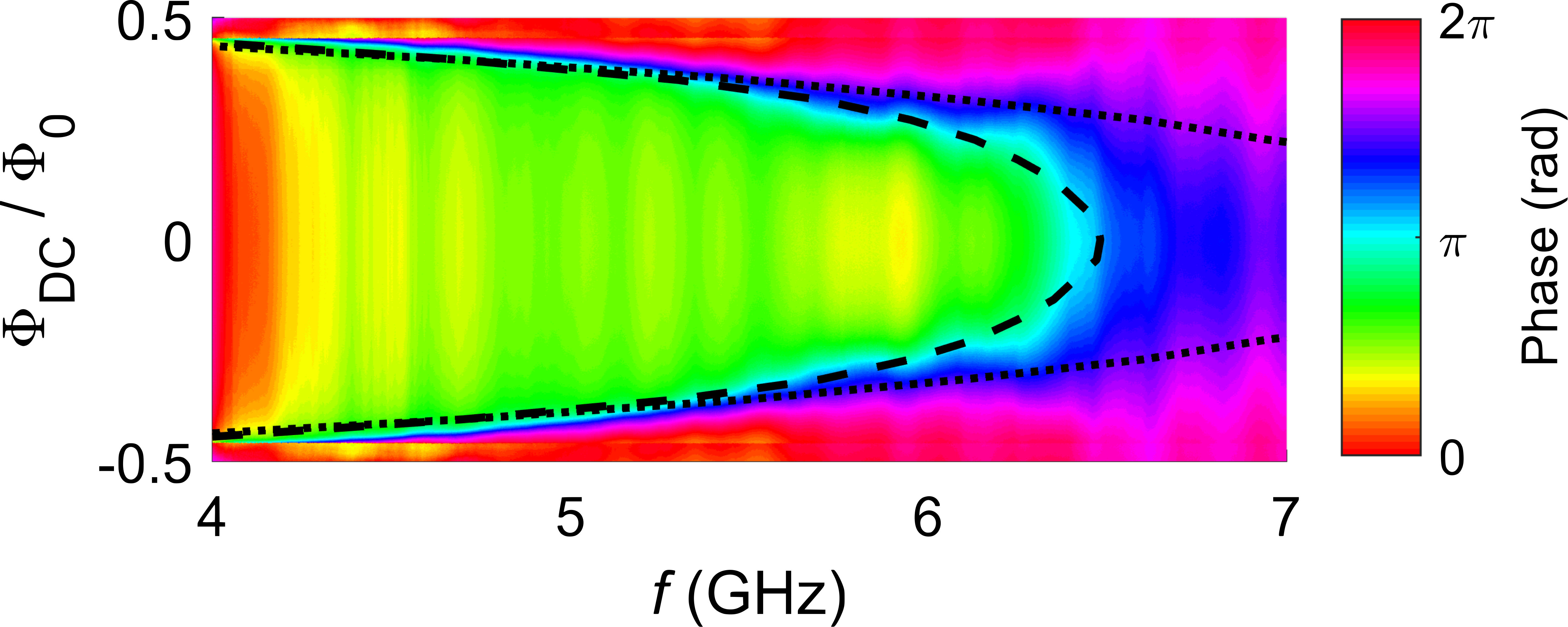 Figure 1
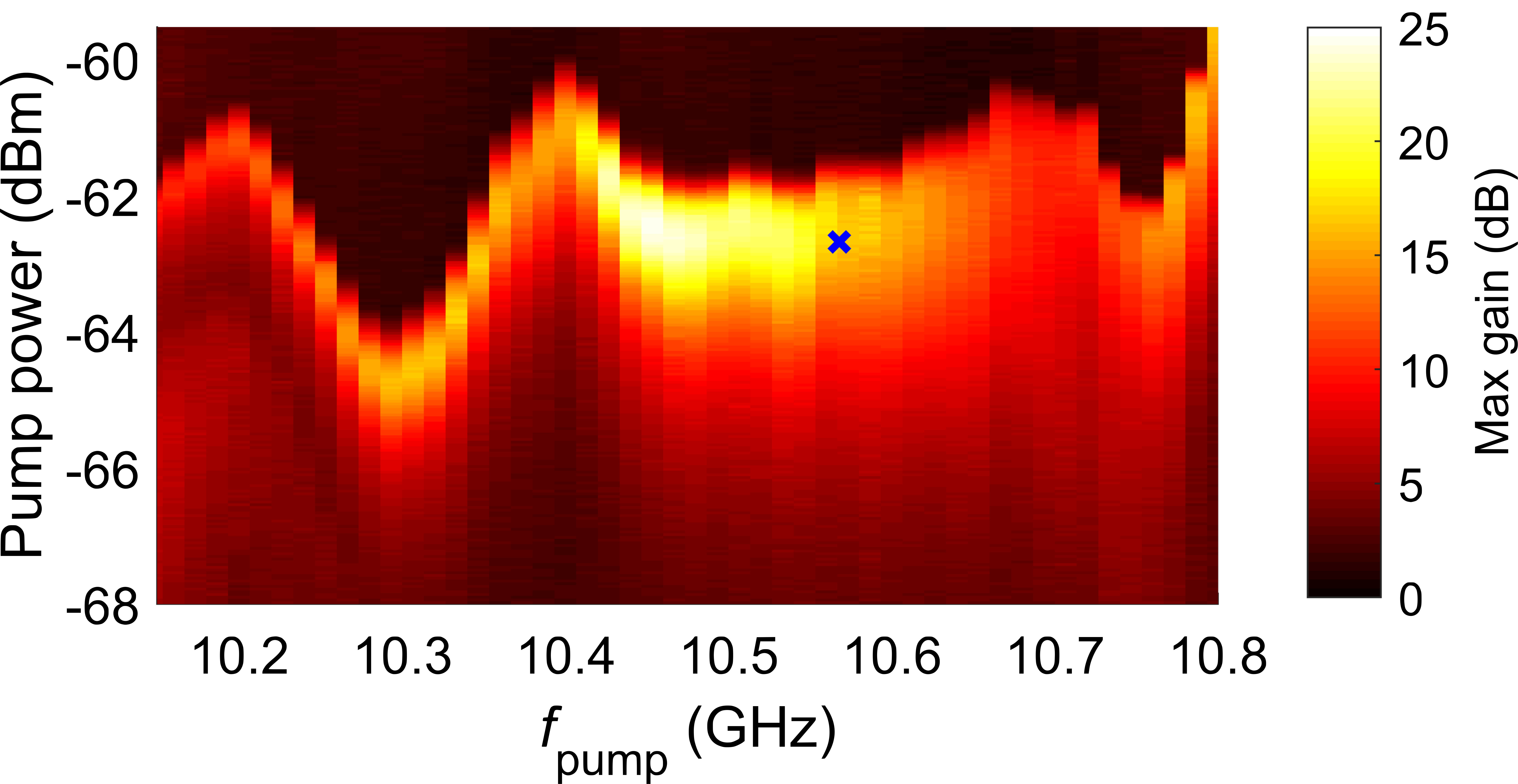 Figure 2
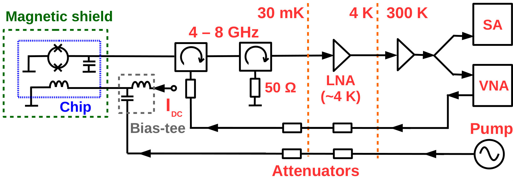 Figure 3
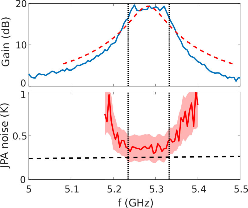 Figure 4
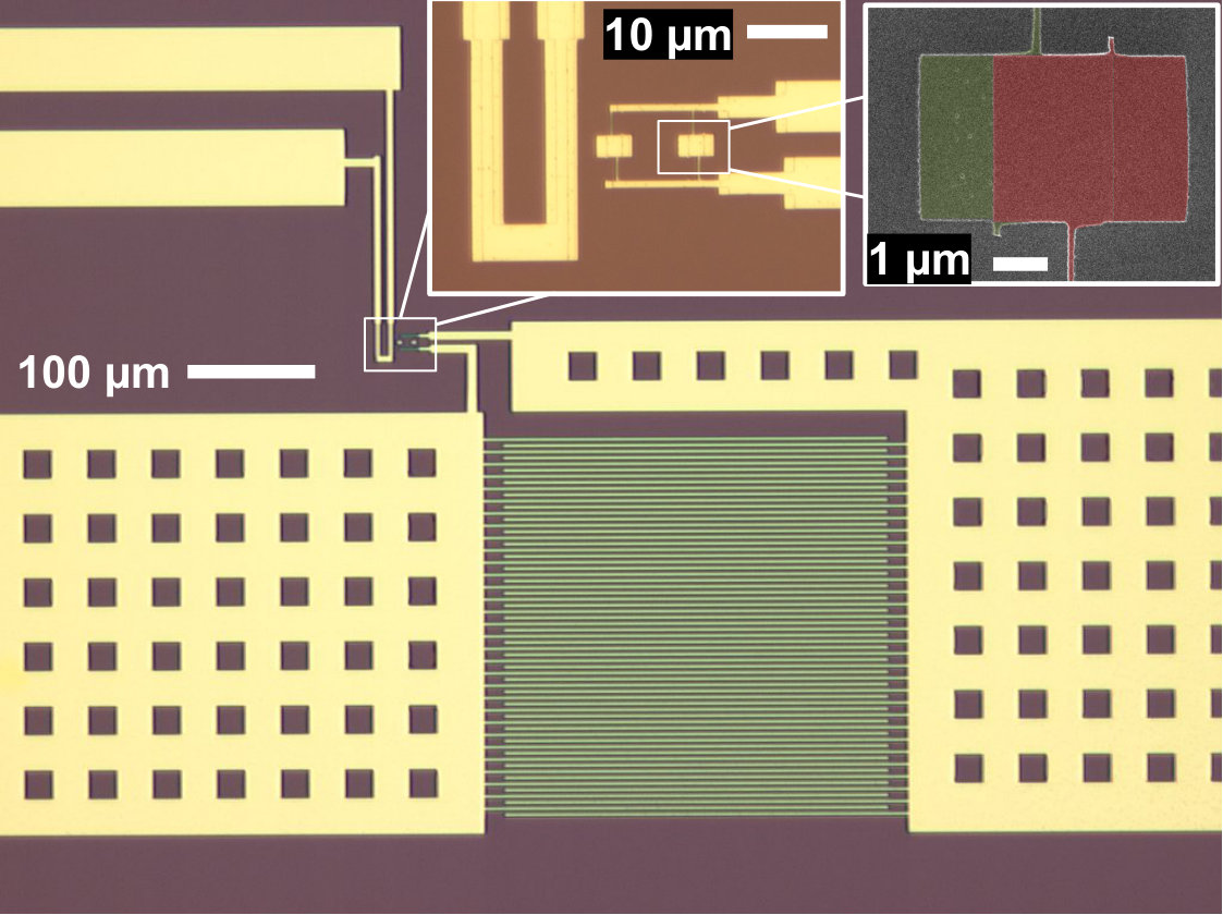 Figure 5
Peer Reviews
No public reviews on file for this paper yet. If you reviewed it on a platform where reviews are public (OpenReview, ICLR, NeurIPS, ICML), you can paste yours below so the community can read it here.
Videos
No videos yet. Explain this paper in a talk, walkthrough, or lecture? Add one.
Broadband lumped-element Josephson parametric amplifier with single-step lithography
T. Elo
Low Temperature Laboratory, Department of Applied Physics, Aalto University School of Science, P.O. Box 15100, FI-00076 AALTO, Finland
T. S. Abhilash
Low Temperature Laboratory, Department of Applied Physics, Aalto University School of Science, P.O. Box 15100, FI-00076 AALTO, Finland
M. R. Perelshtein
Low Temperature Laboratory, Department of Applied Physics, Aalto University School of Science, P.O. Box 15100, FI-00076 AALTO, Finland
Moscow Institute of Physics and Technology, 141700, Russian Federation
I. Lilja
Low Temperature Laboratory, Department of Applied Physics, Aalto University School of Science, P.O. Box 15100, FI-00076 AALTO, Finland
E. V. Korostylev
Moscow Institute of Physics and Technology, 141700, Russian Federation
P. J. Hakonen
Low Temperature Laboratory, Department of Applied Physics, Aalto University School of Science, P.O. Box 15100, FI-00076 AALTO, Finland
Abstract
We present a lumped-element Josephson parametric amplifier (JPA) utilizing a straightforward fabrication process involving a single electron beam lithography step followed by double-angle evaporation of aluminum and in-situ oxidation. The Josephson junctions forming the SQUID are fabricated using bridgeless shadow evaporation technique, which enables reliable fabrication of relatively large () junctions. Our strongly coupled flux-pumped JPA achieves 20 dB gain with 95 MHz bandwidth around 5 GHz, while the center frequency is tunable by more than 1 GHz, with the additional possibility for rapid tuning by varying the pump frequency alone. Analytical calculations based on the input-output theory reproduce our measurement results closely.
Low-noise amplification of microwave signals is a key requirement in numerous experiments in quantum technology, including qubit readout, optomechanics and quantum sensors. Since current state-of-the-art semiconductor amplifiers add 1 – 3 K of noise to the measured signal Schleeh et al. (2012), Josephson parametric amplifiers (JPAs) Zimmer (1967); Yurke et al. (1988), along with other superconducting amplifiers Ho Eom et al. (2012); Lähteenmäki et al. (2012, 2014); Jebari et al. (2018), having added noise close to one quantum have gained significant interest. The active component in a JPA is the nonlinear inductance of a Josephson junction (JJ), modulating the resonance frequency of a resonator, in first realizations formed by a transmission line cavity Yamamoto et al. (2008); Castellanos-Beltran et al. (2008); Bergeal et al. (2010); Simoen et al. (2015). However, the bandwidth of cavity-based JPAs is limited to a few MHz due to the high quality () factor of the cavity.
To achieve higher bandwidths, a lumped-element JPA was introduced Hatridge et al. (2011), where the JJ and a capacitor form a parallel LC resonator, maximizing the ratio of Josephson inductance to the total inductance. The behavior of a lumped element JPA can be tuned over a wide range by changing the coupling strength. Besides high coupled configurationZhou et al. (2014), one can omit the coupling capacitor resulting in a low coupled and wide bandwidth Hatridge et al. (2011); Mutus et al. (2013) of up to 100 MHz, which can be increased further by engineering the impedance of the environment Mutus et al. (2014); Roy et al. (2015). However, these JPAs are relatively complicated to fabricate, requiring deposition of low-loss dielectric for parallel plate capacitor and low-impedance vias Mutus et al. (2013) or optical lithography for niobium followed by e-beam lithography for two aluminum layers Zhou et al. (2014).
We present a lumped-element JPA utilizing a straightforward fabrication process. The JJs, capacitor, flux line and bonding pads are defined in a single e-beam lithography followed by double-angle evaporation of aluminum. We employ a bridgeless shadow evaporation technique Lecocq et al. (2011) allowing us to fabricate JJs with high critical currents by increasing the surface area instead of lowering oxide thickness, which could lead to increased variance of critical currents.
First, we consider the theoretical framework of our lumped-element JPA, operating at frequency , consisting of a non-linear resonator formed by a shunt capacitor and a SQUID which is pumped with external RF magnetic flux through the SQUID at frequency (three-wave mixing). We chose this operation regime, because for a four-wave mixing (typically with a current pump with ) the large amplitude pump is within the amplification bandwidth, whereas the three-wave mixing process separates the pump tone from the amplified signals, therefore simplifying the practical use of the JPA. We can write down the Hamiltonian of a system under study in the rotating wave approximation Lähteenmäki et al. (2013):
[TABLE]
In this formula , where is the resonator frequency, is the strength of pump and is the cavity mode. Solving the Quantum Langevin Equation (QLE) with the Hamiltonian above yields the signal gain as a function of frequency. In QLE we take into consideration a cavity decay rate , which is determined by the JPA quality factor : . Since our JPA is strongly coupled to the environment, its quality factor is dominated by coupling, and therefore ( ). The resulting amplification of the signal at frequency as a function of detuning is given by
[TABLE]
where is the electrical susceptibility of resonator. It can be seen from the equation that gain is achieved at various resonator detunings, but to clarify this dependence we fix the pump power to , corresponding to infinity gain at zero detuning. Now, by substituting , where we introduce , the maximum gain at a given resonator detuning is given by:
[TABLE]
In the high-gain limit we can assume that , and in terms of quality factor this relation can be written as . Consequently, we can express the pump frequency range where the gain exceeds a given value :
[TABLE]
Then, in addition to wide bandwidth, JPA with low quality factor has the advantage of wide tunability by varying the pump frequency. This tuning via is a considerably faster operation than changing the DC flux value. In general, when the pump power is not fixed it is possible to use to evaluate the final maximum gain function of the two parameters controlled in the experiment:
[TABLE]
where . Here if this equation turns into Eq. (3). Note that in the case , meaning zero resonator detuning, gain tends to infinity.
The design of our JPA is shown in Fig. 1. The layout design follows a lumped-element principle: no transmission lines are required since all distances are kept short compared to the wavelength ( at 10 GHz). Instead of a ground plane spreading over the entire chip, we place the SQUID and the capacitor in proximity to two bonding pads. The JPA is tuned and pumped with an external AC+DC flux through the SQUID loop, applied with a loop whose geometry is designed to reduce parasitic coupling to the loop formed by the SQUID and the capacitor.
While the resonance frequency of the JPA is given by , the amplification bandwidth is inversely proportional to quality factor Mutus et al. (2014); Roy et al. (2015), and thus related to critical current of the SQUID as . On the other hand, the saturation power of the JPA is directly proportional to , resulting in a trade-off between bandwidth and saturation power. Moreover, JPAs with low require strong pumping which may cause unwanted nonlinear behavior Roy et al. (2015); Manucharyan et al. (2007). However, in our application wide bandwidth is preferred over high saturation power, and therefore we set , resulting in = 1.2 pF and = 0.8 nH, obtained by applying DC magnetic flux of through a SQUID with total unbiased A.
The capacitor was realized as an interdigital capacitor due to its low losses Bahl (2003) and good suitability to our e-beam lithography process. The capacitor is oriented so that the rotational axis of evaporation angles is perpendicular to the capacitor fingers, allowing proper control over the finger widths. The 1.2 pF capacitor has 62 fingers with 330 m length and 2.4 m width and gap, connected to the bonding pads directly, thus minimizing parasitic inductance. Since large interdigital capacitors may exhibit nonideal behavior at high frequencies, we verified our capacitor design with electromagnetic simulations 111CST Microwave Studio and Sonnet were used for EM simulations.. In addition, EM simulations were used to estimate the total geometric inductance of the JPA device, resulting in less than 10 % of the total inductance at the operating range.
For the Josephson junctions we chose a small critical current density (7 A/) to improve the quality and reproducibility of the JJs. This, combined with the 600 nA critical current of the JJs results in junction area of . Since such JJs are difficult to fabricate with Dolan bridge technique, we employed a bridgeless shadow evaporation process Lecocq et al. (2011), where the layer separation is realized in the leads connecting the JJs: the lines leading up- and downwards from the JJ in Fig. 1 are formed by the first and second aluminum layers, respectively.
The JPAs were fabricated on oxidized silicon substrate with e-beam lithography using double layer resist (Copolymer MMA-MAA 700 nm + PMMA 200 nm) and 100 kV beam to achieve low parasitic undercuts. The process involved a double-angle () evaporation of 75 nm thick aluminum, separated by in-situ oxidation at 15 mbar for 10 min.
Our measurement setup is illustrated in Fig. 2. The measurements were conducted at 30 mK in BlueFors LD-250 dry dilution cryostat. The JPA was protected from external magnetic fields with a cylindrical Cryoperm shield and a superconducting (Pb) inner shield. The DC flux bias and RF pump shared a common on-chip flux line, and the signals were combined by an external bias-tee.
First, we characterized the tunability of the JPA resonance frequency as a function of DC magnetic flux applied through the SQUID loop. The Fig. 3 shows the phase of the reflected signal and the calculated estimates for resonance frequency using both ideal and EM-simulated capacitor model including parasitic inductance. Although our capacitor contains parasitics, we observe that at the desired working point at 5 GHz the deviation between the two capacitor models is negligible, meaning that the capacitor can be considered nearly ideal at those frequencies.
We then characterized the JPA gain at various values of . Our JPA exhibited 13 dB gain at , and the widest tunability was obtained at . The maximum gain at that point is plotted in Fig. 4 as a function of pump frequency and pump power entering the JPA, omitting reflection and finite coupling of the pump tone to the SQUID. The observed variation of the pump power at maximum gain was most likely caused by minor resonances in the flux pumping line, causing the actual RF flux amplitude through the SQUID to fluctuate as a function of the pump frequency at constant applied pump power. It should be noted that the operation frequency can be tuned by several hundred MHz varying the pump frequency alone, as shown in Eq. (4), while additional tunability from 4.8 to 5.8 GHz can be achieved by varying the DC flux as well.
Noise performance of the JPA was characterized with signal-to-noise ratio improvement method, giving noise relative to system noise temperature, which was calibrated separately using Y-factor method with a heated load. Thus, we can estimate the noise temperature of the JPA using the following relationRoy et al. (2015):
[TABLE]
where is the total system noise referred to JPA input port including the noise of the HEMT preamplifier and losses in cables and circulators, is the SNR improvement and is the gain as defined in Eq. (2). Our system noise has a mean value of about 6 K.
The gain and noise characteristics of the JPA in the denoted chosen operating point are shown in Fig. 5. The dashed red line marks the calculated gain outline, showing good agreement with the experiment. In calculations we used for DC flux and for RF flux, the strength of pump was . We attribute the large error in the noise plot to the inaccuracies in cable losses and system noise temperature measurement. Since our design was optimized for wide bandwidth, the determined input power resulting in 1 dB gain compression was dBm, which, although low, is adequate for various experiments.
In summary, we have designed and fabricated a JPA using a straightforward fabrication process with single-step e-beam lithography. The design favoring wide bandwidth over high dynamic range resulted in nearly quantum-limited noise performance with 20 dB gain and 95 MHz bandwidth, which will be useful e.g. in shot noise spectroscopyNieminen et al. (2016) and quantum vacuum measurementsZhong et al. (2013); Lähteenmäki et al. (2016), where signal levels are low. Varying the pump frequency allows rapid tuning of the JPA band center by several hundred MHz. In addition, the bandwidth can be improved further using impedance engineering. Because the JPA is relatively simple to fabricate, the design can be easily modified to meet the requirements of various experimental settings.
We thank A. Lebedev and S. Paraoanu for fruitful discussions. This work was financially supported by the Academy of Finland (projects no. 314448 and 312295), by ERC (grant no. 670743) and by the Ministry of Education and Science of the Russian Federation (grant no. RFMEFI59417X0014). T.E. is grateful to Väisälä foundation of the Finnish Academy of Science and Letters for scholarship. This research work made use of the Aalto University OtaNano/LTL infrasructure which is part of European Microkelvin Platform. Our project also took advantage of equipment at MIPT Shared Facilities Center.
The reference list from the paper itself. Each links out to its DOI / PubMed record.
- 1Schleeh et al. (2012) J. Schleeh, G. Alestig, J. Halonen, A. Malmros, B. Nilsson, P. A. Nilsson, J. P. Starski, N. Wadefalk, H. Zirath, and J. Grahn, IEEE Electron Device Lett. 33 , 664 (2012) . · doi ↗
- 2Zimmer (1967) H. Zimmer, Appl. Phys. Lett. 10 , 193 (1967) . · doi ↗
- 3Yurke et al. (1988) B. Yurke, P. G. Kaminsky, R. E. Miller, E. A. Whittaker, A. D. Smith, A. H. Silver, and R. W. Simon, Phys. Rev. Lett. 60 , 764 (1988) . · doi ↗
- 4Ho Eom et al. (2012) B. Ho Eom, P. K. Day, H. G. Leduc, and J. Zmuidzinas, Nat. Phys. 8 , 623 (2012) . · doi ↗
- 5Lähteenmäki et al. (2012) P. Lähteenmäki, V. Vesterinen, J. Hassel, H. Seppä, and P. Hakonen, Sci. Rep. 2 , 276 (2012) . · doi ↗
- 6Lähteenmäki et al. (2014) P. Lähteenmäki, V. Vesterinen, J. Hassel, G. S. Paraoanu, H. Seppä, and P. Hakonen, J. Low Temp. Phys. 175 , 868 (2014) . · doi ↗
- 7Jebari et al. (2018) S. Jebari, F. Blanchet, A. Grimm, D. Hazra, R. Albert, P. Joyez, D. Vion, D. Estève, F. Portier, and M. Hofheinz, Nat. Electron. 1 , 223 (2018) . · doi ↗
- 8Yamamoto et al. (2008) T. Yamamoto, K. Inomata, M. Watanabe, K. Matsuba, T. Miyazaki, W. D. Oliver, Y. Nakamura, and J. S. Tsai, Appl. Phys. Lett. 93 , 042510 (2008) . · doi ↗