Possible Experimental Realization of a Basic Z2 Topological Semimetal
Erik Haubold, Alexander Fedorov, Igor P. Rusinov, Tatiana V., Menshchikova, Viola Duppel, Daniel Friedrich, Florian Pielnhofer, Richard, Weihrich, Arno Pfitzner, Alexander Zeugner, Anna Isaeva, Setti Thirupathaiah,, Yevhen Kushnirenko, Emile Rienks, Timur Kim, Evgueni V. Chulkov

TL;DR
This paper presents evidence that GaGeTe is a Z2 topological semimetal with unique electronic properties, including multiple charge carriers and a peculiar band structure, which could impact future topological material applications.
Contribution
It provides the first experimental and theoretical demonstration of GaGeTe as a Z2 topological semimetal with distinctive electronic features.
Findings
GaGeTe hosts bulk electrons, holes, and surface electrons.
Band structure calculations reveal a small indirect gap with band inversion.
The material exhibits a unique coexistence of electron and hole carriers at the Fermi level.
Abstract
We report experimental and theoretical evidence that GaGeTe is a basic topological semimetal with three types of charge carriers: bulk-originated electrons and holes as well as surface state electrons. This electronic situation is qualitatively similar to the primer 3D topological insulator Bi2Se3, but important differences account for an unprecedented transport scenario in GaGeTe. High-resolution angle-resolved photoemission spectroscopy combined with advanced band structure calculations show a small indirect energy gap caused by a peculiar band inversion in the \textit{T}-point of the Brillouin zone in GaGeTe. An energy overlap of the valence and conduction bands brings both electron- and hole-like carriers to the Fermi level, while the momentum gap between the corresponding dispersions remains finite. We argue that peculiarities of the electronic spectrum of GaGeTe have a…
Click any figure to enlarge with its caption.
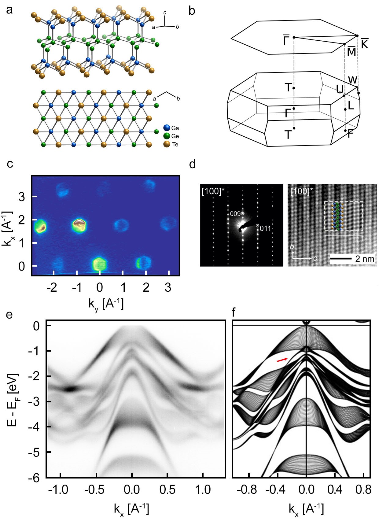 Figure 1
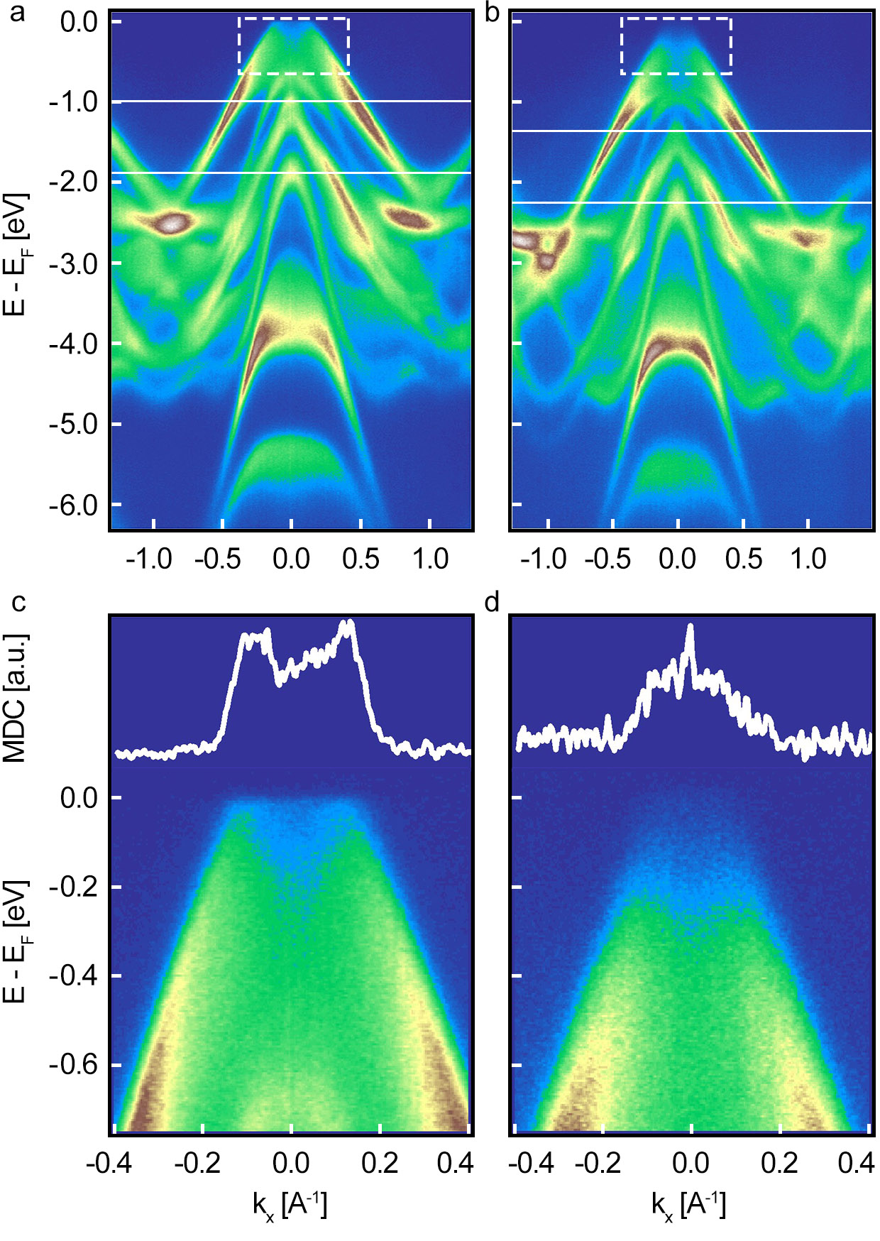 Figure 2
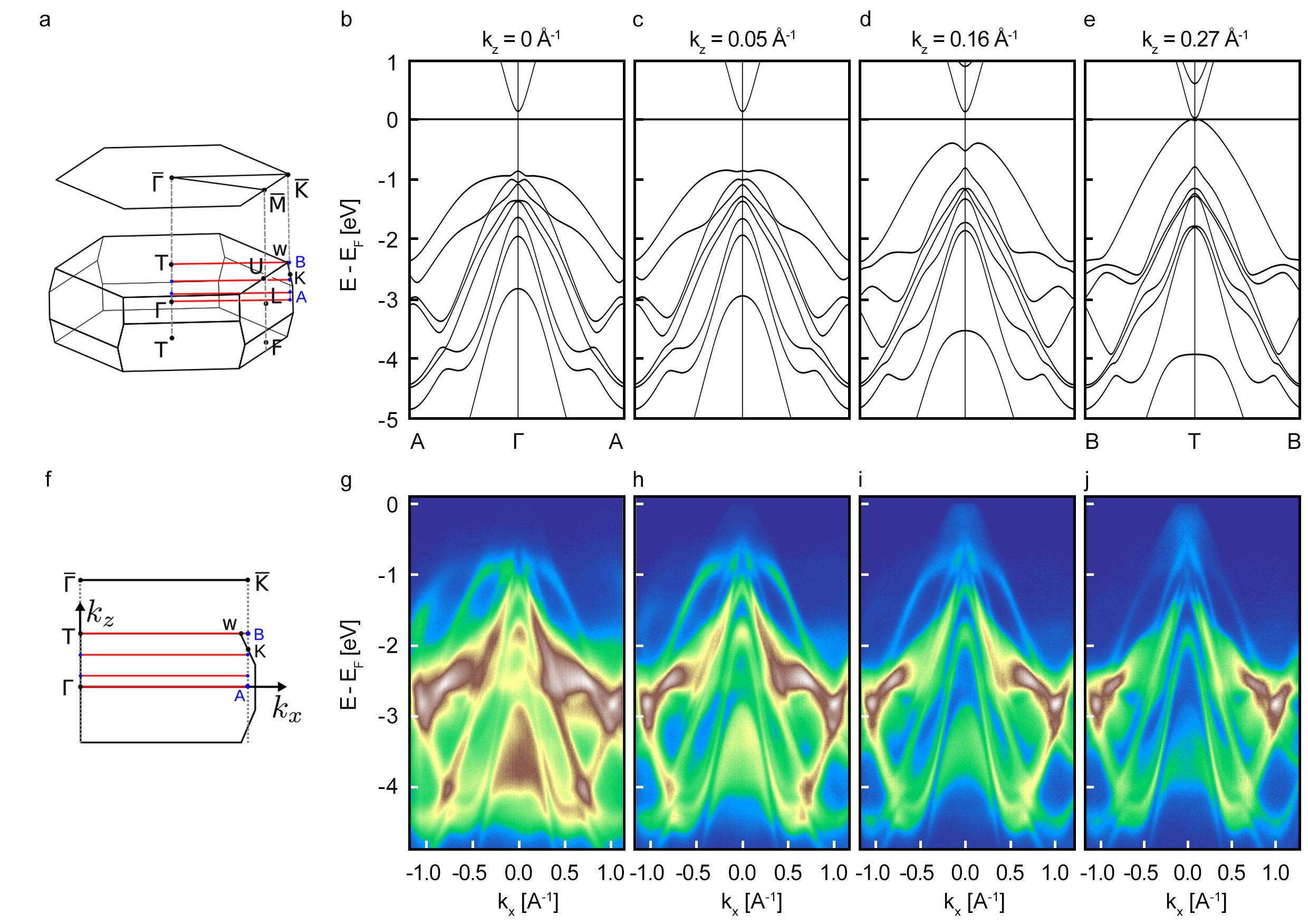 Figure 3
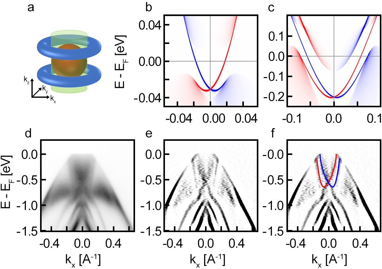 Figure 4
Peer Reviews
No public reviews on file for this paper yet. If you reviewed it on a platform where reviews are public (OpenReview, ICLR, NeurIPS, ICML), you can paste yours below so the community can read it here.
Videos
No videos yet. Explain this paper in a talk, walkthrough, or lecture? Add one.
present address: ]S. N. Bose National Centre for Basic Sciences, Block-JD, Sector-III, Salt Lake, Kolkata 700106, India
Possible Experimental Realization of a Basic Z2 Topological Semimetal
Erik Haubold
Alexander Fedorov
IFW Dresden, Helmholtzstr. 20, 01069 Dresden, Germany
Igor P. Rusinov
Tomsk State University, pr. Lenina 36, 634050 Tomsk, Russia
St. Petersburg State University, Universitetskaya nab. 7/9, 199034 St. Petersburg, Russia
Tatiana V. Menshchikova
Tomsk State University, pr. Lenina 36, 634050 Tomsk, Russia
Viola Duppel
Max Planck Institute for Solid State Research, Heisenbergstr. 1, 70569 Stuttgart, Germany
Daniel Friedrich
Institut für Anorganische Chemie, Universität Regensburg, 93040 Regensburg
Florian Pielnhofer
Max Planck Institute for Solid State Research, Heisenbergstr. 1, 70569 Stuttgart, Germany
Institut für Anorganische Chemie, Universität Regensburg, 93040 Regensburg
Richard Weihrich
Universität Augsburg, Institut für Materials Ressource Management, Universitätsstr. 2, 86135 Augsburg
Arno Pfitzner
Institut für Anorganische Chemie, Universität Regensburg, 93040 Regensburg
Alexander Zeugner
Anna Isaeva
Faculty of Chemistry and Food Chemistry, Technische Universität Dresden, Helmholtzstr. 10, 01069 Dresden, Germany
Setti Thirupathaiah
[
IFW Dresden, Helmholtzstr. 20, 01069 Dresden, Germany
Yevhen Kushnirenko
IFW Dresden, Helmholtzstr. 20, 01069 Dresden, Germany
Emile Rienks
IFW Dresden, Helmholtzstr. 20, 01069 Dresden, Germany
Department of Physics, TU Dresden, 01062 Dresden, Germany
Timur Kim
Diamond Light Source, Harwell Campus, Didcot OX11 0DE, United Kingdom
Evgueni V. Chulkov
Tomsk State University, pr. Lenina 36, 634050 Tomsk, Russia
St. Petersburg State University, Universitetskaya nab. 7/9, 199034 St. Petersburg, Russia
Donostia International Physics Center, Paseo de Manuel Lardizabal 4, 20018 San Sebastian/Donostia, Basque Country, Spain
Departamento de Fisica de Materiales, Facultad de Ciencias Quimicas, and Centro de Fisica de Materiales and Materials Physics Center, University of the Basque Country (UPV/EHU), 20080 San Sebastian/Donostia, Basque Country, Spain
Bernd Büchner
IFW Dresden, Helmholtzstr. 20, 01069 Dresden, Germany
Department of Physics, TU Dresden, 01062 Dresden, Germany
Sergey Borisenko
IFW Dresden, Helmholtzstr. 20, 01069 Dresden, Germany
Abstract
We report experimental and theoretical evidence that \chGaGeTe is a basic topological semimetal with three types of charge carriers: bulk-originated electrons and holes as well as surface state electrons. This electronic situation is qualitatively similar to the primer 3D topological insulator \chBi2Se3, but important differences account for an unprecedented transport scenario in \chGaGeTe. High-resolution angle-resolved photoemission spectroscopy combined with advanced band structure calculations show a small indirect energy gap caused by a peculiar band inversion in the T-point of the Brillouin zone in \chGaGeTe. An energy overlap of the valence and conduction bands brings both electron- and hole-like carriers to the Fermi level, while the momentum gap between the corresponding dispersions remains finite. We argue that peculiarities of the electronic spectrum of \chGaGeTe have a fundamental importance for the physics of topological matter and may boost the material’s application potential.
A variety of materials where topology of the electronic structure plays a special role in transport properties is rapidly growing Ando [2013], Ando and Fu [2015], Armitage et al. [2018]. The envisioned applications of topological materials in novel devices and quantum information technology will be strongly influenced by the fine balance between their charge carriers of various types. In classic 3D topological insulators, like \chBi2Se3, the transport properties are dictated by the non-degenerate massless topological surface states as well as the electron-like carriers from the bulk conduction band Hasan and Kane [2010]. In 3D Dirac or Weyl semimetals, the Fermi surface is formed by single points of band degeneration (type I), or hole and electronic pockets touching in discrete points (type II) Armitage et al. [2018]. A bulk material with a gapped electronic spectrum combining a comparable number of both types of the bulk charge carriers with the spin-momentum locked topological surface states has not yet been accounted for. Here we put forward \chGaGeTe as the first example of such conceptually different electronic situation, i. e. a basic topological semimetal.
The layered compound \chGaGeTe was first synthesized and structurally characterized quite long ago Kra et al. [1977], Fenske and Schnering , and its phonon structure López-Cruz et al. [1984], thermoelectric Drašar et al. [2012] and transport Kucek et al. [2013] properties were consequently studied. However, the first theoretical study of its bulk electronic structure has appeared very recently Pielnhofer et al. [2017] and has sparked strong interest in the surface electronic structure of this material Zhang et al. [2017]. In Pielnhofer et al. [2017] structural and electronic resemblance between a structure fragment of the layered \chGaGeTe bulk and a heavy analogue of graphene, germanene Dávila et al. [2014], has been highlighted. 2D materials with buckled honeycomb atomic arrangements, e.g. silicene, germanene, stanene, are promising for the realization of new devices. For instance, silicene demonstrates such advantages as high carrier mobility, excellent mechanical flexibility and compatibility with existing Si-based electronics. Most recent studies establish theoretically Zhang et al. [2017] and experimentally Wang et al. [2017] that monolayers of \chGaGeTe, namely six-atom-thick sheets (Fig. 1a) held together by van der Waals interaction, can be exfoliated and are also suitable for the fabrication of nanodevices including transistors and photodetectors. Ultrathin films of \chGaGeTe exhibit transport characteristics superior to many other FETs based on 2D-materials, such high hole mobility and good on/off current ratios.
\ch
GaGeTe is not only promising for potential semiconductor applications, but is also intriguing from the fundamental perspective. First-principle calculations performed by co-authors in Ref. Pielnhofer et al. [2017] have shown a possibility of a topological band inversion in its electronic spectrum driven by spin-orbit coupling. The valence and the conduction bands invert at the T-point, opening up a narrow indirect gap of the order of . The bandgap size appeared to be very sensitive to the chosen computational parameters. Earlier published experimental studies of physical properties of \chGaGeTe neither corroborate nor refute this scenario. For instance, an optical study implies that \chGaGeTe is a semiconductor with the band gap of Kucek et al. [2013]. To shed more light on these controversial outcomes of theory and experiment, we have engaged on the present study of high-quality \chGaGeTe single crystals by synchrotron-based angle-resolved photoemission spectroscopy (ARPES) with variable photon energies. We clarify the details of the electronic structure of \chGaGeTe and scrutinize its probable topological nature with an aid of state-of-the-art calculations of its bulk and surface electronic structures.
\ch
GaGeTe crystallizes in a trigonal unit cell (sp. gr. ) that comprises an -stacking of sixtuple layers. High-resolution transmission electron microscopy experiments confirm the ordering along the stacking direction (Fig. 1d). One building unit of \chGaGeTe (Fig. 1a) can be regarded as a corrugated Ge-bilayer (germanene) sandwiched between two \chGaTe sheets of the zincblende type. Bonding within the sixtuple layers is essentially covalent, while the inter-layer interaction is of the van der Waals type. Consequently, the natural cleavage plane of \chGaGeTe crystals is always Te-terminated, which facilitates the interpretation of the photoemission measurements. Cleavage in ultra-high vacuum results in a mirror-like surface which allows to record, in particular, large Fermi surface maps.
One of such FS maps taken using the horizontally polarized photons is shown in Fig. 1c. The FS contour is very small, having the radius of , it is however larger than that of \chBi2Se3 Kordyuk et al. [2011]. The size, the shape and intensity of this contour depends on momentum and thus imply three-dimensionality of the electronic structure: effective k probed by photons with particular energy is always smaller for larger k and k. For example, the signal is nearly absent for the contour at (, ) and its size is smaller for the contour centered at (, ). It means that electron escape depth in this material is sufficient to distinguish between different k’s even using the same photon energy.
We compare the underlying dispersions, experimental and calculated ones, in Fig. 1d and e, respectively. As a first step it is instructive to compare with the k-integrated calculations to find out about the k-resolution mentioned above. Experimental data are taken along the cut running parallel to the direction of the 2D Brillouin zone. The projection of the 3D BZ onto the 2D BZ is shown in Fig. 1b. The overall agreement is remarkable and not only qualitative, especially for the direction: all the dispersions coincide, including the energy positions of the dispersion maxima at zero momentum. The only exception is the two-dimensional band (weak k-dispersion) having a top at \sim$$0.8\text{\,}\mathrm{eV} according to the calculations while experiment shows it reaches the maximum at \sim$$0.65\text{\,}\mathrm{eV} binding energy (see the red arrow in Fig. 1e). One can also notice that the experiment has more spectral weight at particular k values, although an admixture from other k’s is still visible. This observation agrees well with the moderate k-resolution concluded from the Fermi surface map shown in panel c. Within the considered energy range, we note a good agreement between experiment and theory, independent of which exchange-correlation functional, PBE or HSE, is used to describe the occupied electronic structure of \chGaGeTe Pielnhofer et al. [2017].
Now we can address its k dependence in more details by comparing the data collected with differing photon energies. The typical data representing the k behaviour are shown in Fig. 2 and compared with the results of the band structure calculations. Panels a-d show a calculated band structure using the PBE functional. The band inversion manifests itself very clearly in the cuts running through the T-point (Fig. 2d). At other k’s one can still notice the characteristic dip in the quickly dispersing hole-like band. This trend is confirmed by the experimental data shown in panels e-h. These data were measured using the photon energies from (e) to (h) in steps of . The hole-like dispersion is noticeably changing when approaching the Fermi level. In addition to this, one can see that another feature is present at the Fermi level and its intensity is growing together with the intensity of the hole-like feature. There is no energy gap visible between them. At higher binding energies there are bands showing a large k dependency as well, e.g. the bands seen in Fig. 1e,f at at the point. The corresponding intensity redistribution in the experimental data shown in panels e-h of Fig. 2 clearly tracks these changes. As expected, the bands with weaker k dispersion are visible in all energy momentum cuts at approximately the same energies.
Summarizing the experimental observations so far, we can conclude that the energy gap is either very small or absent at all, thus, annulling the earlier beliefs that \chGaGeTe is a wide-gap semiconductor with a gap. This, together with the peculiar shape of the closest to E dispersion of the hole-like band clearly speaks in favour of the band inversion and, subsequently, the topological nature of \chGaGeTe. In this case, the topological surface states are expected.
To clarify whether the PBE-based result, namely the topological band inversion, holds in terms of the gap size, we have carried out typical dosing experiments evaporating potassium on the surface of the sample. The results of these measurements are shown in Fig 3. The dosing turned out to be effective, and we managed to shift the chemical potential by nearly half an eV (Fig. 3a,b). As it was suggested by Fig. 1d,e, the top of the hole-like band was very close to the Fermi level (Fig. 3c,d). According to DFT calculations, in the case of the HSE functional, the band structure is topologically trivial with a rather large direct gap () with the gap extrema located exactly in the T-point of 3D BZ Pielnhofer et al. [2017]. In the case of the PBE functional, the band gap size is smaller (∼) and the gap is indirect, implying the topological character of the electronic spectrum.
In accordance with the PBE-based calculations, we have not observed a large energy gap suggested by other functionals including HSE either. On the other hand, we also have not observed a small direct energy gap between the valence and conduction bands and a sharp electron-like bottom of the conduction band itself, suggested by the PBE calculations. Instead, we detected a spectral density at the Fermi level (Fig. 3d) with the finite momentum width, which stayed nearly constant and increased only slightly up to the highest dosing level. At higher rates the features became too blurred to encourage further dosing. We found out that this intensity could be enhanced using the light of different photon energies, implying that there is indeed no direct gap between the valence and conduction bands and one can safely rule out the scenario with a large gap. The electronic structure of \chGaGeTe is thus characterized by a band inversion and is non-trivial.
We have analysed the topological phase in \chGaGeTe by two methods. At first, the parities of the states at the time-reversal invariant momentum (TRIM) points of the primitive rhombohedral cell were considered. The results establish a non-trivial character of the electronic structure, as characterized by the topological invariant , which originates from a bulk band inversion at the T-point of the 3D Brillouin zone. The edge of the valence zone is constituted by the even states, the s-orbitals of the Ge atoms, whereas the conduction-band edge is composed of the odd states, the Te p-orbitals. Away from the region of the band inversion, the orbital composition of the gap edges is reversed. We also checked the topological nature of \chGaGeTe by varying spin-orbit coupling strength. The gap size decreases down to zero when the spin-orbit coupling strength is diminished to , where is the natural value of the SOC contribution. At smaller , the electronic spectrum is trivial, the gap edges are not inverted, and is equal to 0;(000). Additionally, we also prove the non-trivial topology by the Wilson loop (WL) method proposed in Soluyanov and Vanderbilt [2011], Yu et al. [2011]. It allows to trace the topology of a material graphically. The WL spectra at and are shown in supplementary Data. It is evident that the spectra cross an arbitrary reference line an odd number of times at and an even number of times at . This case corresponds to =1;(001). Also at , both for and the WL bands cross the reference line an even number of times. This finding is also in agreement with the above given analysis of the invariant conducted on the basis of the parity of the wave-functions.
In Fig. 4 we present the data taken using lower photon energies, , to zoom in the region of interest. As we noticed earlier, it is difficult to assign the particular high-symmetry point along the –T pathway to a particular photon energy because of the moderate k-resolution in the case of \chGaGeTe. Also in this case, on one side, the higher intensity of the strongly dispersing hole-like band at the higher binding energies (approx. ) would imply this cut corresponds to the vicinity of the -point; on the other side, the strongest spectral weight at the Fermi level means one is close to the T-point. In any case, now it is clearly seen that the calculations with the experimental lattice parameters do not reproduce the photoemission experiment in full details. The most striking observation is that the electron-like dispersion corresponding to the bottom of the conduction band is clearly seen below the Fermi level. We note that this is not a signature of the n-doping since Figures 1-2 demonstrated that also the valence hole-like band crosses the chemical potential. Taking into account the overall agreement with the calculations on a larger energy scale, we conclude that the deviations preserving a Luttinger count occur. Instead of a semiconductor with a tiny direct gap, experiment shows that \chGaGeTe is a semimetal with the small bulk-originated Fermi surfaces of both types, a hole-like FS, with the shape of a torus due to the crossings of the strongly dispersing hole-like band, and an electron-like FS, with the shape of an ellipsoid or even a sphere, supported by the electron-like conduction band with its minimum below the Fermi level near the T-point. Our calculations demonstrate that the band dispersions in the vicinity of the Fermi energy are extremely sensitive to even miniscule changes in the unit cell parameters and geometry optimization. For instance, the described experimental picture can be confirmed computationally with a slightly extended unit cell parameter , namely, from to . To keep the cell volume constant, the lattice parameter has been contracted from to . In both cases, the material is topological and qualitatively similar surface states should be present. We identify those as straight linear dispersions accompanying the conduction band states down to approx. in the experimental spectra shown in panel d. Second derivative (panel e) helps to distinguish them from the bulk projections of the valence and conduction bands.
Although the situation in \chGaGeTe is qualitatively similar to the simplest 3D topological insulator \chBi2Se3, there are important differences. First is that \chGaGeTe does not have a direct gap and is a semimetal in contrast to \chBi2Se3Nechaev et al. [2013], i.e. the valence and the conduction bands overlap in energy and both cross the Fermi level resulting in small Fermi surfaces. Second, the sizes of an energy gap at a particular k-point and of a momentum gap at particular energy are much smaller: less than and less than respectively, which is in agreement with the calculations shown in Fig. 4. The surface states themselves are less robust than in \chBi2Se3. This is related to the quality of the surface after the cleavage of the sample in ultra-high vacuum. In spite of the layered structure of \chGaGeTe, it is very difficult to obtain a relatively big shiny portion of the atomically clean surface. In such cases the surface states are known to be elusive and require repeating experiments to be detected. One of such successful attempts is documented in Fig. 4. The surface states support another small Fermi surface, which we schematically depict in panel (a) as a cylinder together with the bulk originated 3D Fermi surfaces. Our calculations show that these topological surface states are spin-polarized.
The bulk \chGaGeTe thus emerges as a basic topological semimetal. There is only one Dirac cone formed by the topological surface states per Brillouin zone. Unlike the similar electronic structure of Sb-Bi-Sb heterostructures Takayama et al. [2014], Bihlmayer et al. [2010], the number of bulk charge carriers of the opposite types is the same in \chGaGeTe. As previous Pielnhofer et al. [2017], Zhang et al. [2017], Wang et al. [2017] and this studies have demonstrated, the electronic structure of \chGaGeTe is very sensitive to a number of parameters and therefore is very attractive for nanodevice fabrication. It can be tuned by strain, exfoliation, doping and gating. \chGaGeTe is stable on air, not moisture-senstitive, much more ecologically friendly than compounds containing heavy bismuth. At the same time the monolayer of \chGaGeTe seems to be dynamically and thermodynamically stable at very high temperatures Zhang et al. [2017]. Having such a peculiar Fermi surface (Fig. 4 a) with two 3D sheets and one 2D sheet, the hypothetical shift of the Fermi level can switch the system from having purely bulk n-type charge carriers to having purely p-type ones. In between these two extremes, the presence of the non-degenerate topological surface states with the spin-texture can be exploited.
The individual features of this material thus boost its application potential and have a fundamental importance for the physics of topological matter.
This work was supported under DFG grant BO 1912/7-1, IS 250/2-1 of the SPP 1666 program, RU 776/15-1 of the ERANET-Chemistry program, Tomsk State University Project 8.1.01.2018 and St. Petersburg University Project 15.61.202.2015. The authors acknowledge Diamond Light Source for the beamtime at I05 beamline under proposal SI18586 as well as the BESSY II Berlin for the beamtime at 1 ARPES station under proposals 171-05051CR and 172-05659CR/R.
The reference list from the paper itself. Each links out to its DOI / PubMed record.
- 1Ando [2013] Yoichi Ando. Topological insulator materials. Journal of the Physical Society of Japan , 82(10):102001, 2013. doi: 10.7566/JPSJ.82.102001 .
- 2Ando and Fu [2015] Yoichi Ando and Liang Fu. Topological crystalline insulators and topological superconductors: From concepts to materials. Annual Review of Condensed Matter Physics , 6(1):361–381, 2015. doi: 10.1146/annurev-conmatphys-031214-014501 .
- 3Armitage et al. [2018] N. P. Armitage, E. J. Mele, and Ashvin Vishwanath. Weyl and dirac semimetals in three-dimensional solids. Rev. Mod. Phys. , 90:015001, Jan 2018. doi: 10.1103/Rev Mod Phys.90.015001 . URL https://link.aps.org/doi/10.1103/Rev Mod Phys.90.015001 .
- 4Hasan and Kane [2010] M. Z. Hasan and C. L. Kane. Colloquium: Topological insulators. Rev. Mod. Phys. , 82:3045–3067, Nov 2010. doi: 10.1103/Rev Mod Phys.82.3045 . URL https://link.aps.org/doi/10.1103/Rev Mod Phys.82.3045 .
- 5Kra et al. [1977] G. Kra, R. Eholie, and J. Flahant. Comples Rendus des Seances de l’ Academie des Sciences, Serie C: Science Chimiques , 284:889 – 892, 1977.
- 6[6] Dieter Fenske and Hans Georg Von Schnering. Gagete, eine neue defekt-tetraederstruktur. Angewandte Chemie , 95(5):420–421. doi: 10.1002/ange.19830950516 . URL https://onlinelibrary.wiley.com/doi/abs/10.1002/ange.19830950516 .
- 7López-Cruz et al. [1984] E. López-Cruz, M. Cardona, and E. Martínez. Raman spectrum and lattice dynamics of gagete. Phys. Rev. B , 29:5774–5777, May 1984. doi: 10.1103/Phys Rev B.29.5774 . URL https://link.aps.org/doi/10.1103/Phys Rev B.29.5774 .
- 8Drašar et al. [2012] Č. Drašar, V. Kucek, L. Beneš, and P. Lošták. Thermoelectric properties and nonstoichiometry of gagete. AIP Conference Proceedings , 1449(1):267–270, 2012. doi: 10.1063/1.4731548 . URL https://aip.scitation.org/doi/abs/10.1063/1.4731548 .