Phase Separation in the Vicinity of Fermi Surface Hot Spots
T. Jaouen, B. Hildebrand, M.-L. Mottas, M. Di Giovannantonio, P., Ruffieux, M. Rumo, C. W. Nicholson, E. Razzoli, C. Barreteau, A. Ubaldini, E., Giannini, F. Vanini, H. Beck, C. Monney, P. Aebi

TL;DR
This paper investigates how phase separation near Fermi surface hot spots influences charge-density-wave textures and superconductivity in 1T-TiSe2, revealing a fundamental link between Fermi surface topology and electronic inhomogeneity.
Contribution
It uncovers the intrinsic tendency for electronic phase separation near Fermi surface hot spots in 1T-TiSe2, highlighting the role of Fermi surface topology in CDW texturing.
Findings
Phase separation occurs near Fermi surface hot spots.
Fermi surface topology influences CDW inhomogeneity.
Textured electronic phases are linked to band crossings near the Fermi level.
Abstract
Spatially inhomogeneous electronic states are expected to be key ingredients for the emergence of superconducting phases in quantum materials hosting charge-density-waves (CDWs). Prototypical materials are transition-metal dichalcogenides (TMDCs) and among them, 1-TiSe exhibiting intertwined CDW and superconducting states under Cu intercalation, pressure or electrical gating. Although it has been recently proposed that the emergence of superconductivity relates to CDW fluctuations and the development of spatial inhomogeneities in the CDW order, the fundamental mechanism underlying such a phase separation (PS) is still missing. Using angle-resolved photoemission spectroscopy and variable-temperature scanning tunneling microscopy, we report on the phase diagram of the CDW in 1-TiSe as a function of Ti self-doping, an overlooked degree of freedom inducing CDW texturing. We…
Click any figure to enlarge with its caption.
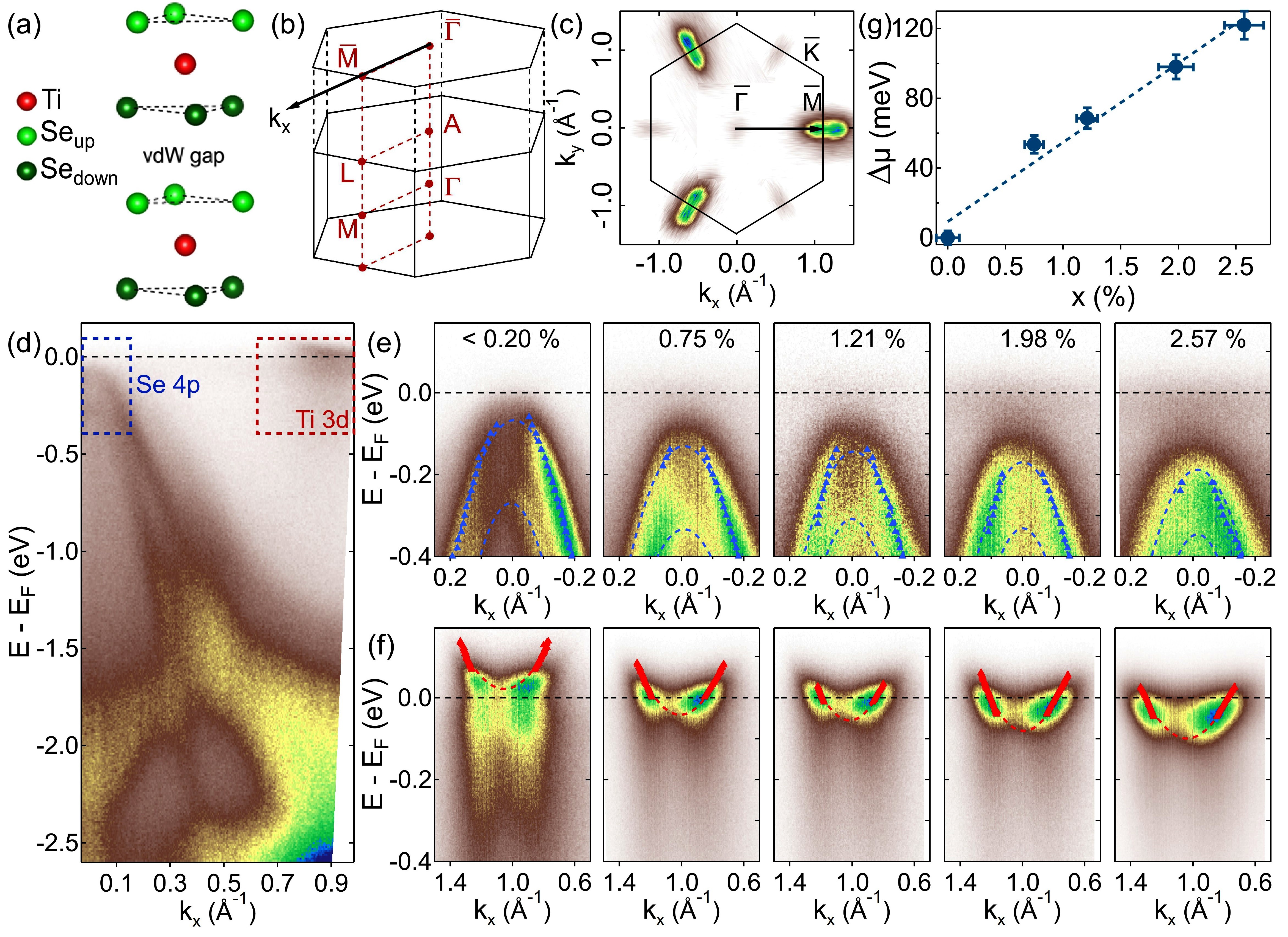 Figure 1
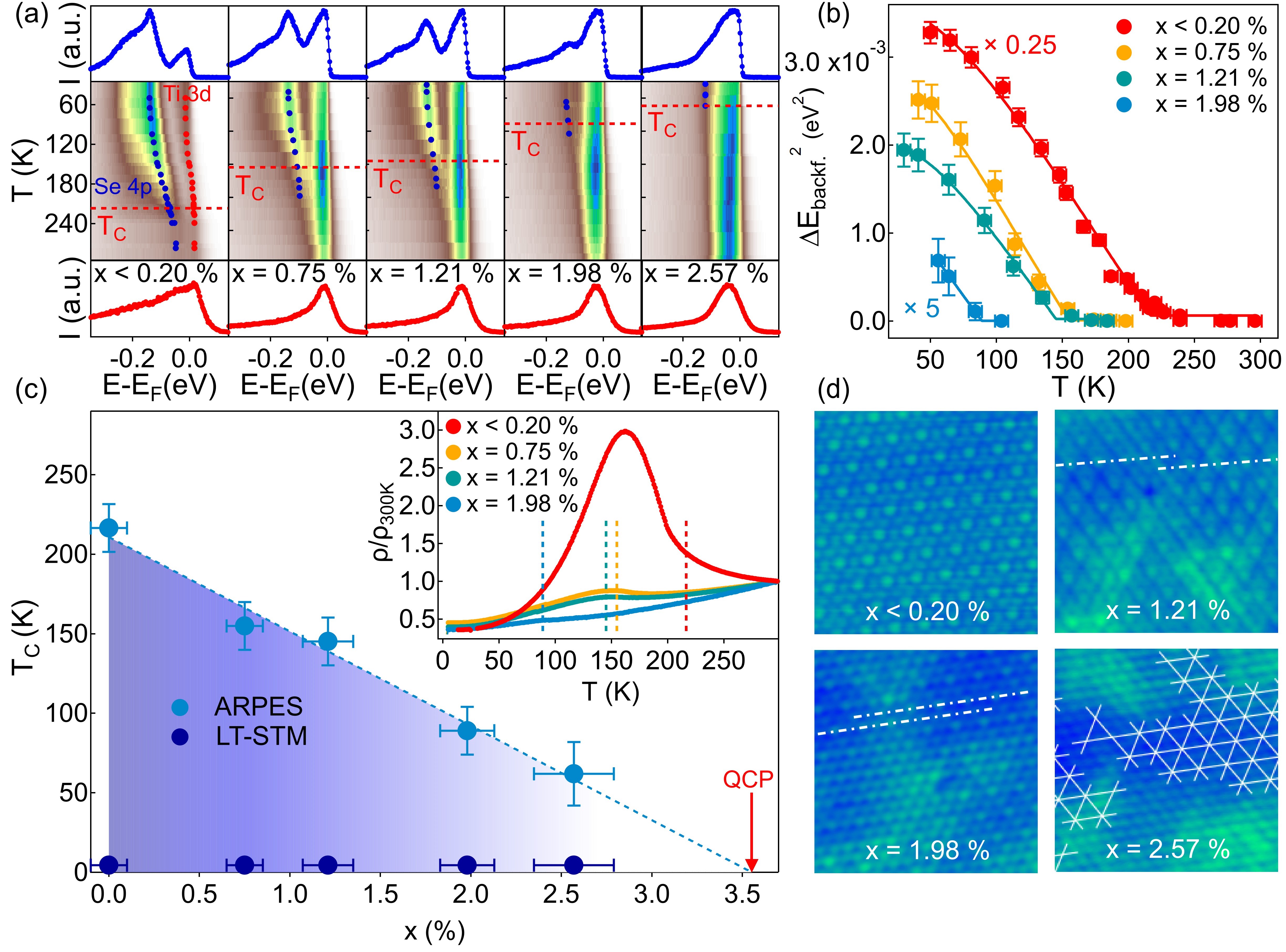 Figure 2
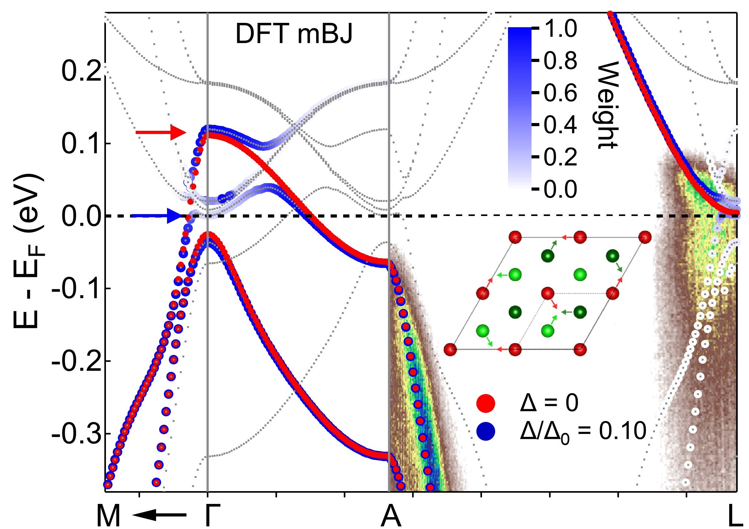 Figure 3
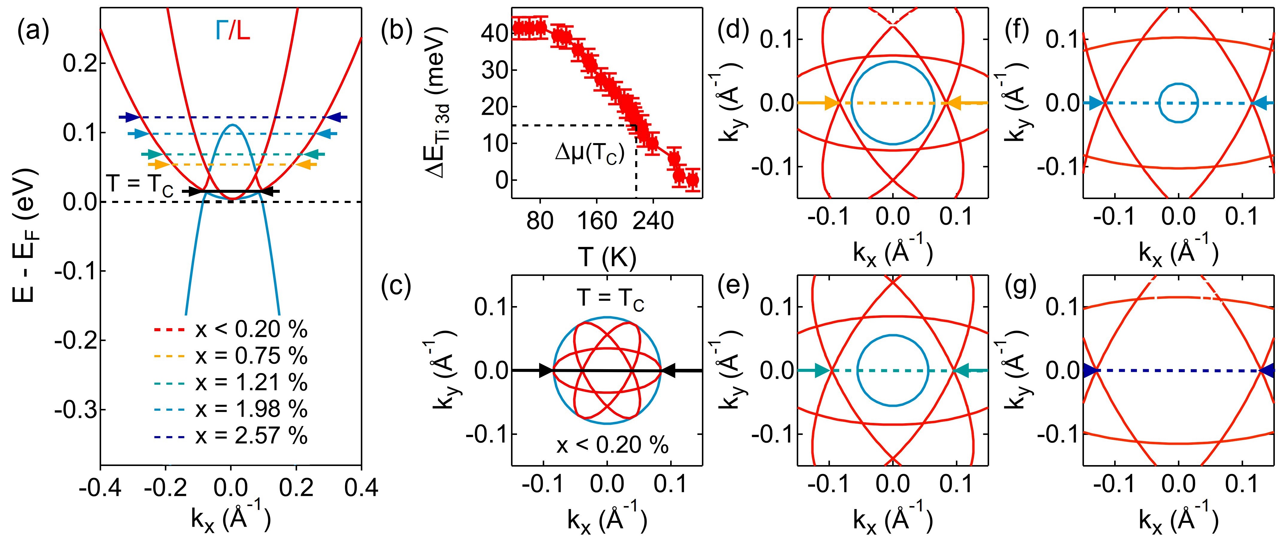 Figure 4
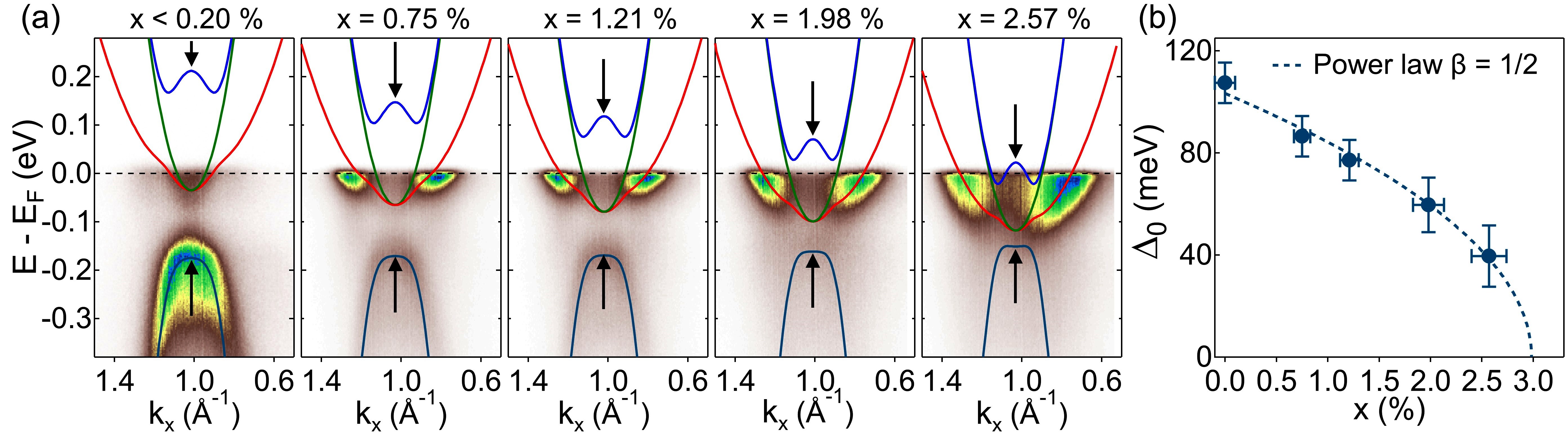 Figure 5
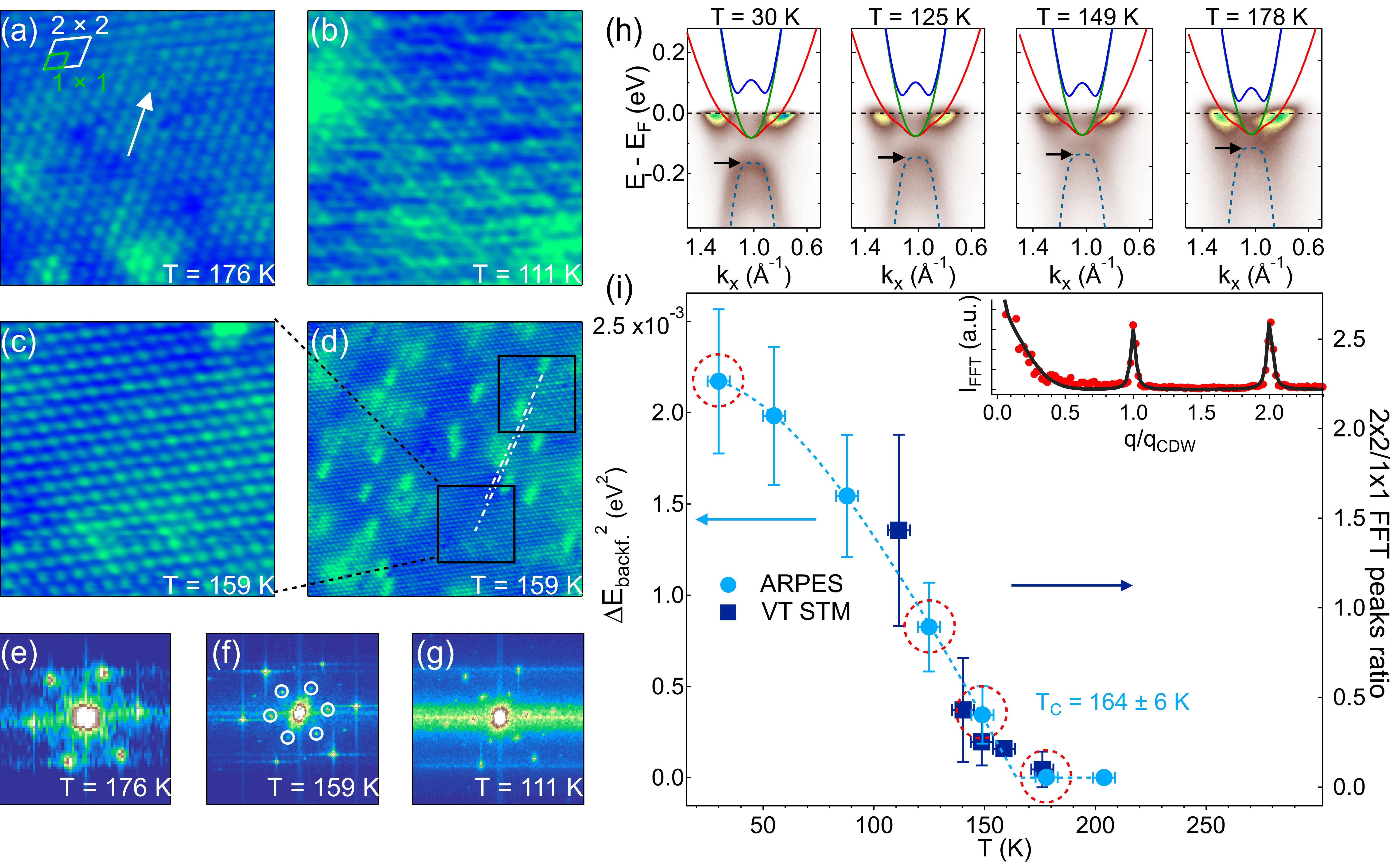 Figure 6
Peer Reviews
No public reviews on file for this paper yet. If you reviewed it on a platform where reviews are public (OpenReview, ICLR, NeurIPS, ICML), you can paste yours below so the community can read it here.
Videos
No videos yet. Explain this paper in a talk, walkthrough, or lecture? Add one.
Phase Separation in the Vicinity of Fermi Surface Hot Spots
T. Jaouen
Corresponding author.
Département de Physique and Fribourg Center for Nanomaterials, Université de Fribourg, CH-1700 Fribourg, Switzerland
B. Hildebrand
Département de Physique and Fribourg Center for Nanomaterials, Université de Fribourg, CH-1700 Fribourg, Switzerland
M.-L. Mottas
Département de Physique and Fribourg Center for Nanomaterials, Université de Fribourg, CH-1700 Fribourg, Switzerland
M. Di Giovannantonio
Empa, Swiss Federal Laboratories for Materials Science and Technology, nanotech@surfaces Laboratory, 8600 Dübendorf, Switzerland
P. Ruffieux
Empa, Swiss Federal Laboratories for Materials Science and Technology, nanotech@surfaces Laboratory, 8600 Dübendorf, Switzerland
M. Rumo
Département de Physique and Fribourg Center for Nanomaterials, Université de Fribourg, CH-1700 Fribourg, Switzerland
C. W. Nicholson
Département de Physique and Fribourg Center for Nanomaterials, Université de Fribourg, CH-1700 Fribourg, Switzerland
E. Razzoli
Quantum Matter Institute, University of British Columbia, Vancouver, BC, Canada V6T 1Z4
Department of Physics and Astronomy, University of British Columbia, Vancouver, BC, Canada V6T 1Z1
C. Barreteau
Department of Quantum Matter Physics, University of Geneva, 24 Quai Ernest-Ansermet, 1211 Geneva 4, Switzerland
A. Ubaldini
Department of Quantum Matter Physics, University of Geneva, 24 Quai Ernest-Ansermet, 1211 Geneva 4, Switzerland
E. Giannini
Department of Quantum Matter Physics, University of Geneva, 24 Quai Ernest-Ansermet, 1211 Geneva 4, Switzerland
F. Vanini
Département de Physique and Fribourg Center for Nanomaterials, Université de Fribourg, CH-1700 Fribourg, Switzerland
H. Beck
Département de Physique and Fribourg Center for Nanomaterials, Université de Fribourg, CH-1700 Fribourg, Switzerland
C. Monney
Département de Physique and Fribourg Center for Nanomaterials, Université de Fribourg, CH-1700 Fribourg, Switzerland
P. Aebi
Département de Physique and Fribourg Center for Nanomaterials, Université de Fribourg, CH-1700 Fribourg, Switzerland
Abstract
Spatially inhomogeneous electronic states are expected to be key ingredients for the emergence of superconducting phases in quantum materials hosting charge-density-waves (CDWs). Prototypical materials are transition-metal dichalcogenides (TMDCs) and among them, 1-TiSe2 exhibiting intertwined CDW and superconducting states under Cu intercalation, pressure or electrical gating. Although it has been recently proposed that the emergence of superconductivity relates to CDW fluctuations and the development of spatial inhomogeneities in the CDW order, the fundamental mechanism underlying such a phase separation (PS) is still missing. Using angle-resolved photoemission spectroscopy and variable-temperature scanning tunneling microscopy, we report on the phase diagram of the CDW in 1-TiSe2 as a function of Ti self-doping, an overlooked degree of freedom inducing CDW texturing. We find an intrinsic tendency towards electronic PS in the vicinity of Fermi surface (FS) ”hot spots”, i.e. locations with band crossings close to, but not at the Fermi level. We therefore demonstrate an intimate relationship between the FS topology and the emergence of spatially textured electronic phases which is expected to be generalizable to many doped CDW compounds.
Introduction
It is well established that electronic phase separation (PS) at the nanometer scale can emerge from competing short-range and long-range interactions and is accompanied by charge inhomogeneity especially in doped systems Li et al. (2015); Mamin et al. (2018). This has been studied in the context of so-called Coulomb-frustration where the competition between the long-range Coulomb interaction, enhanced due to excess charge, and surface energy effects control the characteristic size of the phase-separated pattern Ortix et al. (2008). PS has been demonstrated to lie, for example, at the heart of the magnetoresistance manganite Dagotto (2005), and high- cuprate physics Campi et al. (2015). Another important materials class exhibiting phase diagrams including intertwined charge-density-waves (CDWs), Mott states and superconductivity is the family of layered transition-metal dichalcogenides (TMDCs) Morosan et al. (2006); Sipos et al. (2008); Kusmartseva et al. (2009).
Among them, 1-TiSe2 is a prototypical material with a 2 2 2 commensurate CDW (CCDW) occuring at 200 K and hosting superconductivity under pressure, Cu-doping or electrical gating Kusmartseva et al. (2009); Morosan et al. (2006); Li et al. (2015). The emergence of superconductivity is currently thought to relate to a change in the nature of the CDW from CCDW to incommensurate (ICDW) Kogar et al. (2017a); Joe et al. (2014), passing through a nearly-commensurate intermediate regime (NCCDW) constituted of CCDW domains separated by atomically sharp domain walls (DWs), or discommensurations, hosting excess electrons Chen et al. (2019); Yan et al. (2017); Novello et al. (2017).
Intercalation of Ti dopants in the van der Waals (vdW) gap of the 1-TiSe2 structure [see Fig. 1(a)] is known to occur depending on the crystal growth temperature Di Salvo et al. (1976), and is found even in the best available crystals. Although not superconducting, Ti self-doped 1-TiSe2 crystals have also shown to exhibit a spatially inhomogeneous landscape ultimately leading to nanoscale PS between CDW domains and non-distorted 1 1 phase Hildebrand et al. (2016, 2017, 2018). As we will show, most of the debate surrounding the semimetallic or semiconducting character of the 1-TiSe2 in the high-temperature phase and the underlying origin of the CDW phase transition Rossnagel (2011); Kogar et al. (2017b) are related to the electron-doping nature of such defects. This, in addition to the fluctuating nature of the CDW at room-temperature (RT) made the Fermi surface (FS) topology in the normal state of pristine 1-TiSe2 elusive until now.
Combining angle-resolved photoemission spectroscopy (ARPES), low- and variable-temperature scanning tunneling microscopy (LT-, VT-STM), we study 1-TiSe2 crystals containing low concentrations of native Ti intercalants and focus on the temperature ()-driven and concentration ()-induced CDW transition and suppression. We demonstrate that in pristine 1-TiSe2 the CDW phase transition occurs at a temperature where the chemical potential matches the electron and hole band crossings (defined as FS ”hot spots”) in the hidden semimetallic normal state. In Ti-intercalated samples, the electron-hole band crossings move below the Fermi level due to rigid electron doping. For locally recovering FS hot spots, the system undergoes PS accompanied by charge inhomogeneities. Finally, VT-STM measurements reveal the real-space emergence of the CDW upon temperature lowering and uncover its inhomogeneous nature. The demonstrated PS in a wide region of the (-) phase diagram is shown to primarily rely on the - and -dependences of the chemical potential, i.e. of the FS topology. Our study reinforces the key role of the FS topology for driving not only the CDW instability in 1-TiSe2 but also phase-separated states that emerge in a large class of TMDCs upon doping or pressure Qiao et al. (2017); Liu et al. (2016); Ang et al. (2012); Xu et al. (2010); Sipos et al. (2008); Hu et al. (2007).
Rigid doping by Ti intercalation
In the 1 1 1 normal state, the 1-TiSe2 low-energy electronic states consist of a Se 4 hole pocket at and Ti 3 electron pockets at the three equivalent points of the three-dimensional Brillouin zone (BZ) [see Fig. 1(b)]. At the CDW transition, the and the points are connected by the three new reciprocal lattice -vectors corresponding to the doubling of the lattice periodicity. Figure 1(c) and 1(d) respectively show the RT FS and the corresponding =0 Å*-1* cut for pristine 1-TiSe2. In a free-electron final-state picture He-I ARPES (=21.22 eV) mainly probes the 1-TiSe2 initial states close to the - high-symmetry line of the BZ [see Fig. 1(b)] Pillo et al. (2000). Details of the experimental method are given in Appendix A and procedures for the ARPES data analysis are described elsewhere Mottas et al. (2019). For pristine 1-TiSe2, the hole band at [Fig. 1(e), left panel] is below the Fermi level () (with the top of the band at 672 meV binding energy) and the Ti 3 electron pocket at [Fig. 1(f), left panel] is only thermally occupied and lies 21 meV above . The observed spectral weight centered at 80 meV below the Ti 3 band manifests CDW correlations already at RT Monney et al. (2012a). In fact, the -vectors of the 2 2 2 CDW connect the and points of the BZ. The CDW therefore manifests itself via umklapp, or backfolding, of the Se 4 hole band at to [visible in Fig. 1(f), left].
Figures 1(e), (f) show RT-ARPES intensity map as a function of Ti self-doping (from left to right) at the and points of the BZ, respectively. We notice that our first Ti doping of 0.750.1 already moves the electron pocket below thereby occupying it. The evolution of the hole and electron band extrema extracted from the momentum distribution curves (MDC) fitted as a function of doping (overlaid on the data) further shows that a rigid band model of electron doping applies with the chemical potential , which is linearly raised up by 122 meV between pristine and =2.57 [see Fig. 1(g)].
Phase diagram
Focusing on the impact of electron-doping on the CDW phase transition, we show, in Fig. 2(a), -dependent energy distribution curve (EDC) maps extracted from measurements such as shown in Fig. 1(f), as a function of (from left to right). For each , lower and upper panels respectively show the RT and lowest-T EDCs. For each doping, we see the -dependent energy shifts of the Se 4 backfolded band, (blue dots on the EDC maps), which relate to the CDW order parameter evolutions and allow for determining the transition temperatures () within a BCS-like scheme [onset points of the BCS-like fits in Fig. 2(b)] Monney et al. (2010); Mottas et al. (2019). The impact of doping is visible on the lowest-T EDCs [Fig. 2(a)] with the gradual disappearance of the backfolded band with increased Ti concentration as well as on the EDCs maps which show a decrease of , namely 217 K, 155 K, 145 K, 89 K and 62 K for our increasingly doped samples (see the red-dashed horizontal lines).
Figure 2(c) shows the summary of the - phase diagram of Ti-doped 1-TiSe2. The CDW is suppressed by Ti-intercalation with that linearly decreases with suggesting a quantum critical point (QCP) at =3.550.18 . The observed linear dependence of on the Ti-concentration is well described within a Hertz-Millis picture of quantum critical scaling Hertz (1976); Millis (1993), where the power-law exponent of the -dependence of in mean-field theory is =1, with and that correspond to the exponent of the correlation length and the dynamical critical exponent, respectively. Note that our ARPES-deduced values closely match the ones obtained from the minima in in the -dependent resistivity curves [see inset Fig. 2(c)] Di Salvo et al. (1976). Furthermore, our QCP value is in perfect agreement with the one estimated by Di Salvo et al. from stoichiometry data and resistivity measurements by considering that the presence of holes is fundamental to the formation of the superlattice and that intercalated-Ti atoms increase the number of electrons and decrease the number of holes of the -doped semimetallic normal state Wilson et al. (1978); Di Salvo et al. (1976).
In real-space, we can associate the decrease of to the recently demonstrated CDW patterning with Ti-doping Hildebrand et al. (2016). Figures 2(d) shows 5.5 5.5 nm2 STM images of the 1-TiSe2 surface as a function of Ti-intercalated concentration. Whereas for 0.20 , the 2 2 CDW modulation can be well identified on the whole image through the presence of maxima of the charge density every second atom, in Ti-intercalated samples, DWs, where the phase of the order parameter jumps by , proliferate (see the dotted-dashed white lines). As a function of Ti concentration, the 2 2 commensurate domain size shrinks and non-reconstructed 1 1 regions start to coexist with 2 2 domains, as small as the CDW coherence length, in a phase-separated pattern [see the bottom panels of Fig. 2(d)] Hildebrand et al. (2016). We will now show that the spatial texturing of the CDW, characterized by the emergence of NCCDW and PS with , and its suppression at the QCP both rely on the FS topology in the normal state.
Room-temperature pseudogap state and hidden FS
The semimetallic or semiconducting nature of 1-TiSe2 still remains under debate although it has been heavily investigated in the last decades. Transport measurements Di Salvo et al. (1976); Wilson et al. (1978) as well as recent optical spectroscopy and conductivity studies Li et al. (2007); Velebit et al. (2016), all concluded on a semimetallic normal state with electron-hole band overlap -100 meV. However, three-dimensional momentum-resolved ARPES measurements have reported RT values of bandgap up to 150 meV Rossnagel et al. (2002); Kidd et al. (2002); Zhao et al. (2007); Rasch et al. (2008); Chen et al. (2016); Watson et al. (2019). One should recall that ARPES alone does not allow for the quantification of the bare gap of the non-distorted phase in 1-TiSe2. It probes the ”pseudogap” state as manifested in all ARPES studies by the presence of diffuse backfolded band intensities and suppression of spectral weight originating from CDW fluctuations already present at RT Monney et al. (2015); Borisenko et al. (2008); Pillo et al. (1999).
The situation becomes evident using DFT calculations (see Appendix B). They reveal the hidden FS topology of the normal state and the dramatic effects of CDW fluctuations on the topmost hole-band at . Figure 3 shows DFT-calculated band structures of 1-TiSe2 along the --- path of the 3D BZ for the 1 1 1 normal state (red band structure) and an only slightly distorted structure (grey-white-blue band structure) with respect to the atomic displacements of the 2 2 2 periodic lattice distortion (PLD, shown in the inset) as determined by Di Salvo et al. Di Salvo et al. (1976), and calculated for 10 of the full PLD. This slight displacement mimics the dynamic umklapp effects associated with the Kohn anomaly, occuring above Holt et al. (2001); Weber et al. (2011). We observe the appearance of the folded band structure because , and become symmetry-equivalent (grey dotted bands) while the new spectral weight (see the color scale, from white to blue) mainly remains concentrated close to the unreconstructed (red) dispersion Voit et al. (2000).
Also superimposed on Fig. 3 are the RT ARPES measurements that mainly probe the - direction of the BZ. The top of the calculated Se 4 bands has been aligned with the experimental one at by shifting DFT by 24 meV. DFT very well reproduces not only our measured in-plane band dispersions but also those reported along - in the most recent -resolved ARPES studies Chen et al. (2016); Watson et al. (2019). However we see that CDW fluctuations have a strong impact on the - -dispersion that becomes strongly renormalized as indeed measured in Refs. Chen et al. (2016); Watson et al. (2019). This occurs due to the dynamical folding of the CDW band structure and pseudogap openings between the hybridized Se 4 and Ti 3 bands (also manifested at by the diffuse backfolded Se 4 bands coming from ).
Given the dispersion of the topmost hole band along - in the non-distorted phase, the DFT-calculated 1 1 1 state is semimetallic with an electron-hole band overlap of -107 meV defined as the energy difference between the top of the hole pocket at [red arrow in Fig. 3] and the bottom of the electron pocket at . Note that the out-of-plane dispersion of the hole band is crucial for the 3D component of the CDW -vectors that give rise to the 2 2 2 superlattice. At RT, the CDW fluctuations hide the true 1-TiSe2 normal state for ARPES, which rather probes a ”pseudogap” state (i.e. the blue band structure) with the bottom of the pseudogap at that corresponds to the top of the hole pocket [blue arrow on Fig. 3 along the - path of the BZ] reported in the ARPES experiments until now.
Fermi surface hot spots
Let us now start with the 1-TiSe2 semimetallic normal state as obtained from our combined ARPES and DFT analysis [Fig. 4(a)]. To facilitate the discussion, we superimpose the dispersions of the hole pocket (located at , blue line) and the ones of the three-equivalent electron pockets (located at the points, red lines) folded to by the three CDW -vectors. Note that the lightest electron band is made of two of the symmetry-equivalent elliptical electron pockets.
At RT, is placed near the lowest electron-hole band crossing (exactly 15 meV below). It raises up within the bandstructure by lowering the temperature due to the effect of the Fermi-Dirac cutoff on the overlapping hole and electron bands with different effective band masses. This temperature-dependence can be tracked in -dependent ARPES measurements through the shift of the bottom of the Ti 3 band at [red dots in Fig. 2(a), left panel] Monney et al. (2010). Interestingly, this shift is such that, at =, closely matches the lowest electron- and hole-band crossing as predicted in a recent theoretical paper Chen et al. (2018) [see Fig. 4(b)].
As discussed in Ref. Monney et al. (2012b), no true nesting (i.e. connection of large parallel segments of the FS via the CDW -vectors) is necessary for driving the CDW transition in 1-TiSe2. Rather, as confirmed here and depicted Fig. 4(c), FS hot spots at the crossings of the electron-and hole-bands (see arrows which point at two of the six crossing points) produce the instability with a wave vector corresponding to the commensurate CDW. The relevance of the hot spot physics is also corroborated by a recent optical conductivity study Velebit et al. (2016). It has been not only demonstrated that the non-metallic -dependence of transport properties in the high-temperature semimetallic phase comes from the anomalous -variation of the hole and electron scattering rates, but has also reported an equal contribution of the two types of carriers to the conductivity near due to dominant intervalley scattering in the CDW precursor regime.
With electron doping, we immediately see that the electron-hole band crossings move below [see the coloured dashed lines and arrows in Fig. 4(a)] and that a Lifshitz transition characterized by the loss of the hole pocket from the FS is expected close to a critical doping associated with the QCP [Fig. 4(d)-(g)]. Also, our LT-STM measurements revealed that with increased intercalated-Ti doping, the system undergoes a series of phase transitions from an homogeneous state to a phase-separated one, passing through a NCCDW regime [see Fig. 2(d)].
Imperfect nesting
Imperfect nesting mechanisms, based on a model of Rice Rice (1970), have been proposed for explaining the emergence of inhomogeneous electronic states upon doping in various materials such as chromium alloys, iron-based superconductors, or doped graphene bilayers Rakhmanov et al. (2013, 2013). In such models, the nesting of an electron- and a hole-band is imperfect in the sense that both bands have spherical (i.e. almost parallel) FSs with slightly different radii whose mismatch is proportional to the doping Rakhmanov et al. (2017). In this context, it has been shown that the uniform ground state is unstable with respect to PS in a wide portion of the (, ) plane, because it becomes more favourable for the system to break up into two phases with the better or worse nesting and having different densities of itinerant electrons Rakhmanov et al. (2017). Furthermore, depending on the level of doping and the value of with respect to the order parameter, it has been shown that either the system forms DWs where the doped charge is accumulated and inside which the gap vanishes locally (low doping) Gor’kov and Teitel’baum (2010); Burkhardt and Rainer (1994), or hosts a phase-separated state (high doping).
Therefore, since nesting is replaced by FS hot spots for driving the CDW transition in 1-TiSe2, we propose, in analogy with the imperfect nesting model, that the uniform CCDW ground state is unstable with respect to PS in the vicinity of these FS hot spots. While the increase of doping moves the electron-hole band crossings below , locally, FS hot spots still exist due to PS accompanied by charge inhomogeneity. In the spatial regions with lower charge carrier densities, the CDW phase is still promoted whereas regions with higher charge carriers densities are either DWs in the NCCDW regime or non-reconstructed 1 1 domains in the phase-separated state on the verge of the QCP, where the Lifshitz transition in the normal state occurs Bianconi et al. (2015).
Doping-induced CCDW-ICDW transition
At LT, the evolution of the 1-TiSe2 CDW phase upon Ti doping is shown in Figures 5(a) at the point. Near- dispersions calculated within an effective Hamiltonian model of four bands (see Appendix C), interacting through the LT CDW order parameter , are also superimposed. While the CDW suppression with doping is evident through the suppression of the backfolded CDW band spectral weight and the closing of the CDW gap [see the black arrows in Fig. 5(a)], the mean-field-like evolution of with [Fig. 5(b)] is in perfect agreement with the theory of the CCDW-ICDW transition for 1-TiSe2 upon doping as recently developed within a McMillan’s Ginzburg-Landau framework Chen et al. (2019); McMillan (1975, 1976). Indeed, the lock-in energy, which controls the umklapp energy gain of locking to the commensurate structure, is proportional to the square of Di Salvo et al. (1976) and is closely linked to the electron density ( in a rigid-band model)Chen et al. (2019). As a consequence, is expected to vary with as in Fig. 5(b). Moreover, it has been predicted that a Coulomb-frustrated 2D charged system hosting a second-order phase transition with an order parameter undergoes a series of different PSs when the temperature decreases Mamin et al. (2018); Kabanov et al. (2009), which we will address via -dependent STM in the following.
Phase separation around
As an ultimate confirmation of the mechanism at work, we thus performed VT-STM measurements of lightly-doped (=0.57 0.07 , =1646 K) 1-TiSe2 to probe the real-space emergence of the CDW with . Figures 6(a)-(b) show 5.5 5.5 nm2 STM images, above and below as obtained using ARPES. Whereas at =111 K, the CDW is fully present [see Fig. 6(b)], interestingly, we see on Fig. 6a) that for temperatures higher than local CDWs have developed (white arrow). Approaching [Fig. 6(c)-(d)], we can further recognize the typical landscape of nanoscale PS with phase-shifted CDW domains embedded in the non-distorted 1 1 phase, as in the case of stronger doped crystals at the lowest temperatures Hildebrand et al. (2016). The CDW domains have droplike morphologies on the scale of tens of nanometers with sharp boundaries indicating strong surface energies, which is also consistent with a Coulomb-controlled mechanism of PS Ortix et al. (2008). The temperature evolution of the ()/() Fast-Fourier-Tranform (FFT) spot ratios [Fig. 6(e)-(g)] is further found to closely follow the mean-field -dependence of the order parameter extracted from ARPES [see arrows in Fig. 6(h)], reflecting the increase of the lock-in energy upon cooling. Our VT-STM measurements thus reveal the inhomogeneous nature of the CDW emergence, the static origin of the folding of the Se 4 bands visible just above in ARPES [right panel Fig. 6(h)], and demonstrate that even at such a low Ti-doping, the -evolution of the CDW towards a long-range ordered state at LT intrinsically occurs through the succession of PS and NCCDW.
It should be mentionned that quenched disorder can alter purely Coulomb-frustrated electronic configurations Campi et al. (2015); Dagotto et al. (2003). Looking at the real-space CDW pattern morphology Fig. 6(d) and 2(d), we notice that the electron-rich bright regions locating the Ti-intercalated atoms are spatially anticorrelated with the CDW domain configuration. Unlike Cu in superconducting 1-CuxTiSe2 crystals Spera et al. (2019), Ti-intercalation not only provides electrons to the Fermi sea, but also induces localized 3 impurity states close to responsible for the formation of Ti-Ti-Ti covalent centers, strong local distortions the TiSe6 octahedra Hildebrand et al. (2017), and CDW domains pinning. Therefore, given the strong similarity between the electronic impact of Cu and Ti on the CDW when intercalated within the 1-TiSe2 vdW gap Qian et al. (2007); Zhao et al. (2007), an open question remains as to the extent to which the disorder introduced by native low-concentration Ti defects is detrimental for the emergence of superconductivity in Cu-intercalated crystals. In any case, it calls for considering an additional self-doping axis in the associated phase diagram Kogar et al. (2017a) and opens the door for further exploration.
Conclusion
We combine ARPES, LT- and VT-STM to obtain complementary momentum- and real-space insights into the CDW phase transition of the prototypical TMDC 1-TiSe2 natively containing low concentrations of Ti intercalants. We report persistent nanoscale PS in an extended region of the phase diagram and demonstrate that it relies on the - and -dependences of and the related FS topologies. Our work sheds light on intrinsic impurities as previously overlooked degrees of freedom for the understanding of inhomogeneous electronic landscapes associated to the emergence of superconductivity such as in 1-TiSe2 upon Cu intercalation or pressure. More generally, through the generic case of 1-TiSe2, our study extends the concept of imperfect nesting and induced electronic phase texturing to a wide class of TMDCs.
I Appendix A: Experiment
The 1-TiSe2 single crystals were grown at 590 \celsius, 700 \celsius, 770 \celsius, 860 \celsius, and 900 \celsius by iodine vapor transport, therefore containing increasing concentrations of Ti doping atoms Di Salvo et al. (1976). The Ti concentrations are 0.20 , 0.750.1 , 1.210.14 , 1.980.15 and 2.570.22 , respectively, as determined by STM Hildebrand et al. (2016). The low-temperature (4.5 K), respectively, variable-temperature constant current STM images were recorded using an Omicron LT-STM and VT-STM with bias voltage applied to the sample, after cleaving in-situ below 10*-7* mbar at room temperature. The base pressure during experiments was better than 5 10*-11* mbar. The temperature-dependent ARPES measurements were carried out using a Scienta DA photoelectron analyzer with He-I radiation as excitation source (= eV, SPECS UVLS with TMM 304 monochromator). The total energy resolution was 12 meV.
II Appendix B: Computational method
The DFT-calculated unfolded band structure of the 2 2 2 CDW phase has been performed within the the WIEN2K package Blaha et al. (2001), using the modified Becke-Johnson (mBJ) exchange potential in combination with local density approximation (LDA) correlation Tran and Blaha (2009); Koller et al. (2012), and including spin-orbit coupling. The parameter in mBJ was fixed for all calculations at 1.40, value determined to give the best agreement with the measured normal-state band structure of the pristine 1-TiSe2 and a minimum of the total energy for atomic displacements corresponding to the PLD as proposed by Di Salvo Di Salvo et al. (1976). The system was modeled using a 2 2 2 superstructure of 8 unit cells of TiSe2 with lattice parameters set to ==3.54 Å and =6.01 Å Di Salvo et al. (1976). The calculated band structures were unfolded using the FOLD2BLOCH package Rubel et al. (2014).
III Appendix C: Band simulations
The model from which the near- dispersions describing ARPES of self-doped 1-TiSe2 have been computed includes three dimensional and anisotropic electronic bands, which are obtained by fitting the ARPES dispersions at room temperature and considering DFT band structure calculations along . It has been shown that the electronic structure of 1-TiSe2 in the reconstructed phase can be well described by a Hamiltonian that has the following matrix form Monney et al. (2009),
[TABLE]
where is the order parameter and describes the coupling strength between a single valence band at and the three symmetry equivalent conduction bands () at the three points. The band dispersions for the normal state have been chosen of the form
[TABLE]
which describe well the bands near their extrema as they are measured in ARPES experiment. The unit vectors and , pointing along the long and short axis of the ellipses, respectively, form a local in-plane basis for the electron pockets at the different points. Thus, and where the CDW wave vectors are and . The , and are the effective masses of the valence band holes and of the conduction band electrons along the long and short axis of the electron pockets, respectively. The hopping parameters and represent the amplitudes of the dispersions perpendicular to the surface and is the distance in reciprocal space between and . The parameters and are the band extrema. We define a valence band maximum lying at 110 meV above at the point, a dispersion of 43 meV, Ti 3 conduction band minima at 4 meV above and a dispersion of 30 meV, yielding a semimetallic band structure with a gap of -107 meV (i.e. a band overlap of 107 meV). The band effective masses , and have been fixed to their experimental values as obtained from parabolic fits of the MDCs maxima extracted from the ARPES spectra measured at RT. The effective masses values were -0.28 0.02, 2.50.5, and 0.43 respectively where is the free electron mass. Note that the effective masses coming from DFT are -0.3 and 2.2 for the hole and electron pockets, respectively. Once the coupling between the valence and conduction bands takes a finite value, the valence band gets backfolded to and the conduction bands get backfolded to and other points. The positions of the calculated four bands are complicated functions of which nevertheless drastically simplify exactly at giving Monney et al. (2009), Therefore, in a photoemission experiment, we can extract the order parameter from the shift of the backfolded valence band, corrected by the -induced chemical potential shift using,
[TABLE]
with .
IV Acknowledgments
This project was supported by the Fonds National Suisse pour la Recherche Scientifique through Div. II. E. Razzoli acknowledges support from the Swiss National Science Foundation (SNSF) Grant No. P300P2-164649. We would like to thank C. Berthod and F. Weber and G. Kremer for motivating discussions. Skillful technical assistance was provided by F. Bourqui, B. Hediger and O. Raetzo.
The reference list from the paper itself. Each links out to its DOI / PubMed record.
- 1Li et al. (2015) L. J. Li, E. C. T. O’Farrell, K. P. Loh, G. Eda, B. Özyilmaz, and A. H. Castro Neto, Nature (London) 529 , 185 (2015) . · doi ↗
- 2Mamin et al. (2018) R. F. Mamin, T. S. Shaposhnikova, and V. V. Kabanov, Phys. Rev. B 97 , 94415 (2018) . · doi ↗
- 3Ortix et al. (2008) C. Ortix, J. Lorenzana, and C. D. Castro, J. Phys. Condens. Matter 20 , 434229 (2008) .
- 4Dagotto (2005) E. Dagotto, Science 309 , 257 (2005) . · doi ↗
- 5Campi et al. (2015) G. Campi, A. Bianconi, N. Poccia, G. Bianconi, L. Barba, G. Arrighetti, D. Innocenti, J. Karpinski, N. D. Zhigadlo, S. M. Kazakov, M. Burghammer, M. v. Zimmermann, M. Sprung, and A. Ricci, Nature (London) 525 , 359 (2015) . · doi ↗
- 6Morosan et al. (2006) E. Morosan, H. W. Zandbergen, B. S. Dennis, J. W. G. Bos, Y. Onose, T. Klimczuk, A. P. Ramirez, N. P. Ong, and R. J. Cava, Nat. Phys. 2 , 544 (2006) . · doi ↗
- 7Sipos et al. (2008) B. Sipos, A. F. Kusmartseva, A. Akrap, H. Berger, L. Forró, and E. Tutiš, Nat. Mater. 7 , 960 (2008) . · doi ↗
- 8Kusmartseva et al. (2009) A. F. Kusmartseva, B. Sipos, H. Berger, L. Forró, and E. Tutiš, Phys. Rev. Lett. 103 , 236401 (2009) . · doi ↗