Heterostructures of graphene and hBN: electronic, spin-orbit, and spin relaxation properties from first principles
Klaus Zollner, Martin Gmitra, Jaroslav Fabian

TL;DR
This paper uses first-principles calculations to analyze the electronic and spin relaxation properties of graphene/hBN heterostructures, revealing tunable spin lifetimes and anisotropy influenced by stacking, interlayer distance, and electric fields.
Contribution
It introduces a minimal tight-binding model for graphene/hBN heterostructures and explores how stacking, interlayer distance, and electric fields affect spin-orbit coupling and spin relaxation.
Findings
Spin lifetimes are in the nanosecond range, matching experiments.
Spin relaxation anisotropy is giant near charge neutrality and tunable by electric field.
Orbital and SOC parameters depend strongly on stacking and electric field.
Abstract
We perform extensive first-principles calculations for heterostructures composed of monolayer graphene and hexagonal boron nitride (hBN). Employing a symmetry-derived minimal tight-binding model, we extract orbital and spin-orbit coupling (SOC) parameters for graphene on hBN, as well as for hBN encapsulated graphene. Our calculations show that the parameters depend on the specific stacking configuration of graphene on hBN. We also perform an interlayer distance study for the different graphene/hBN stacks to find the corresponding lowest energy distances. For very large interlayer distances, one can recover the pristine graphene properties, as we find from the dependence of the parameters on the interlayer distance. Furthermore, we find that orbital and SOC parameters, especially the Rashba one, depend strongly on an applied transverse electric field, giving a rich playground for spin…
Click any figure to enlarge with its caption.
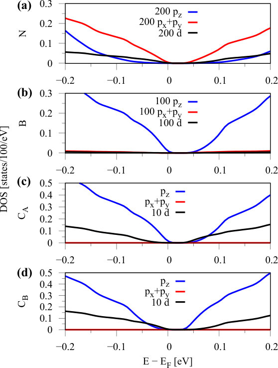 Figure 1
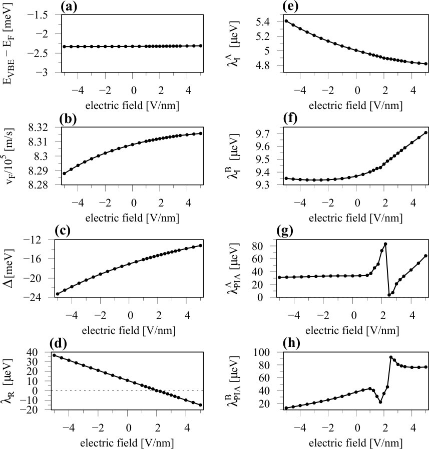 Figure 2
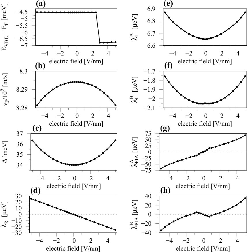 Figure 3
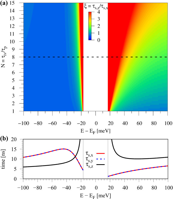 Figure 4
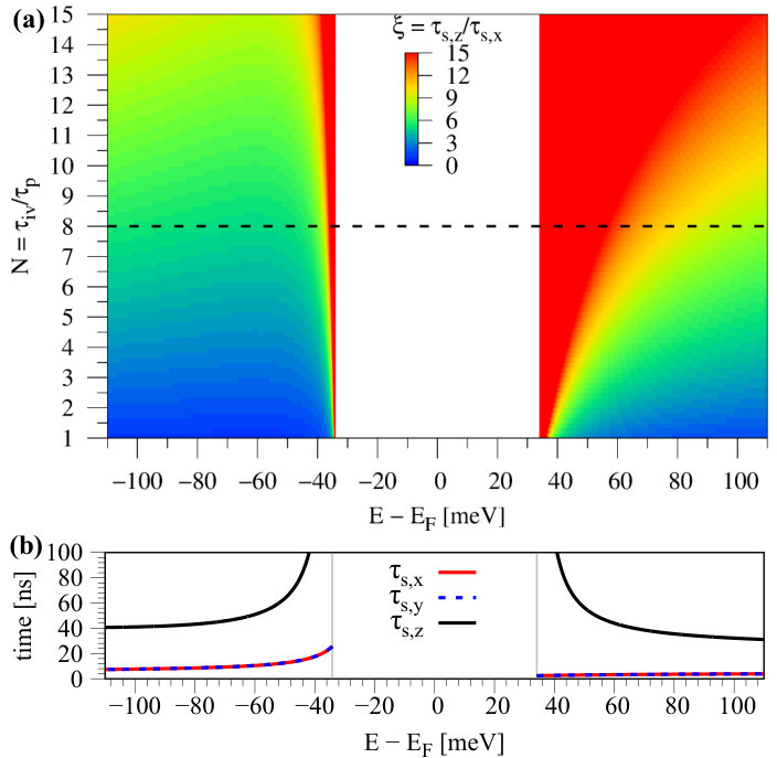 Figure 5
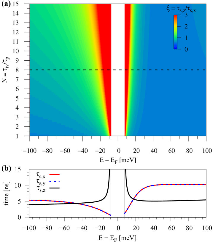 Figure 6
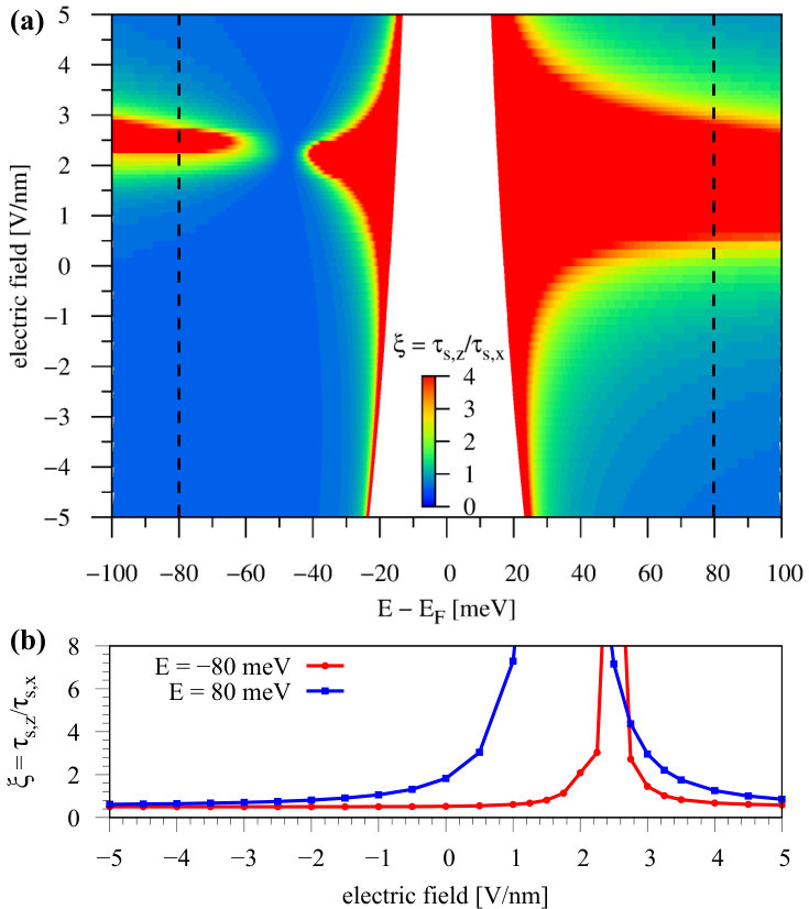 Figure 7
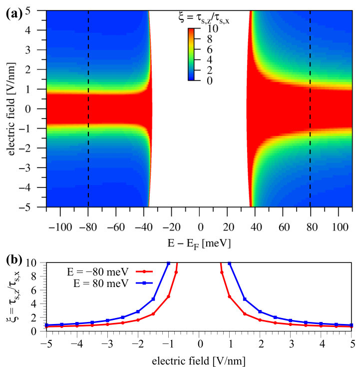 Figure 8
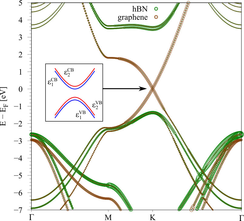 Figure 9
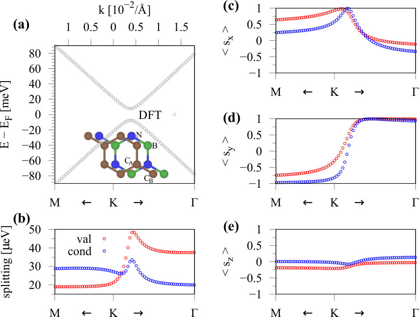 Figure 10
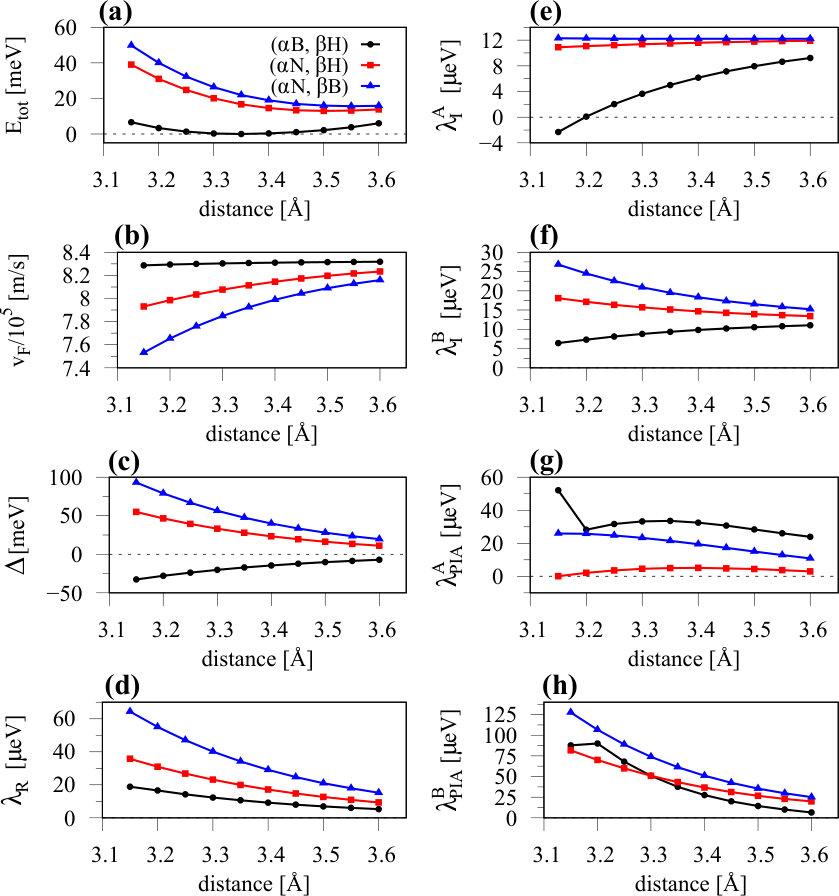 Figure 11
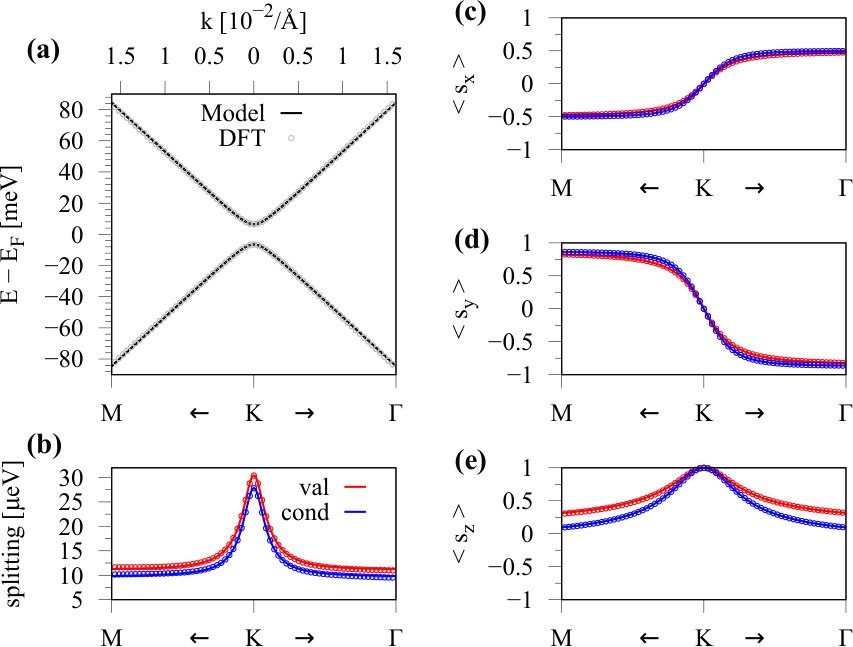 Figure 12
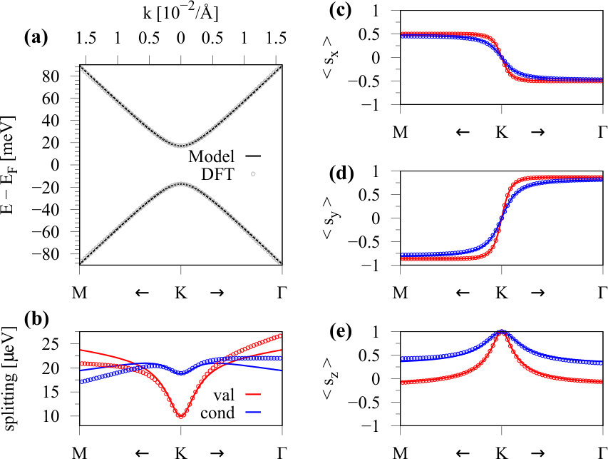 Figure 13
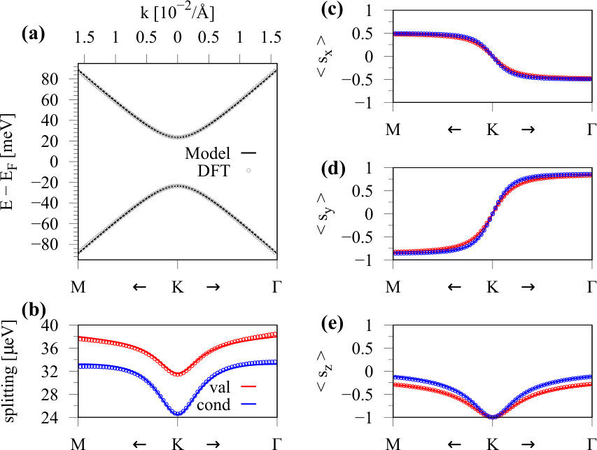 Figure 14
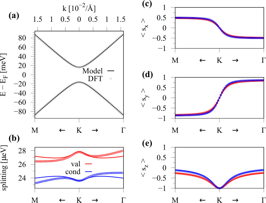 Figure 15
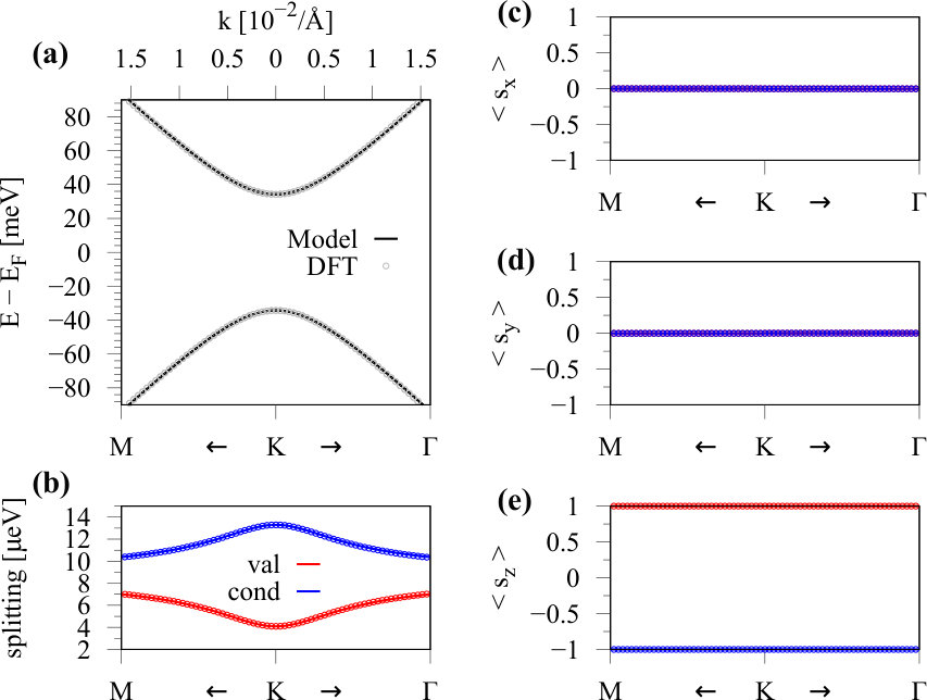 Figure 16
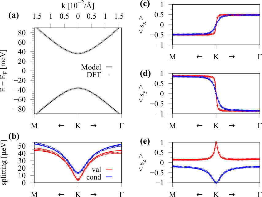 Figure 17
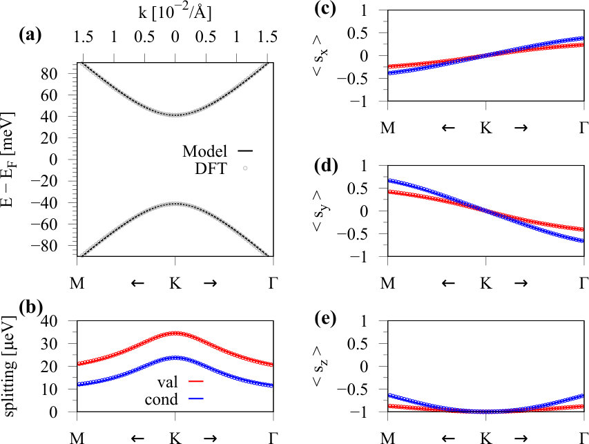 Figure 18
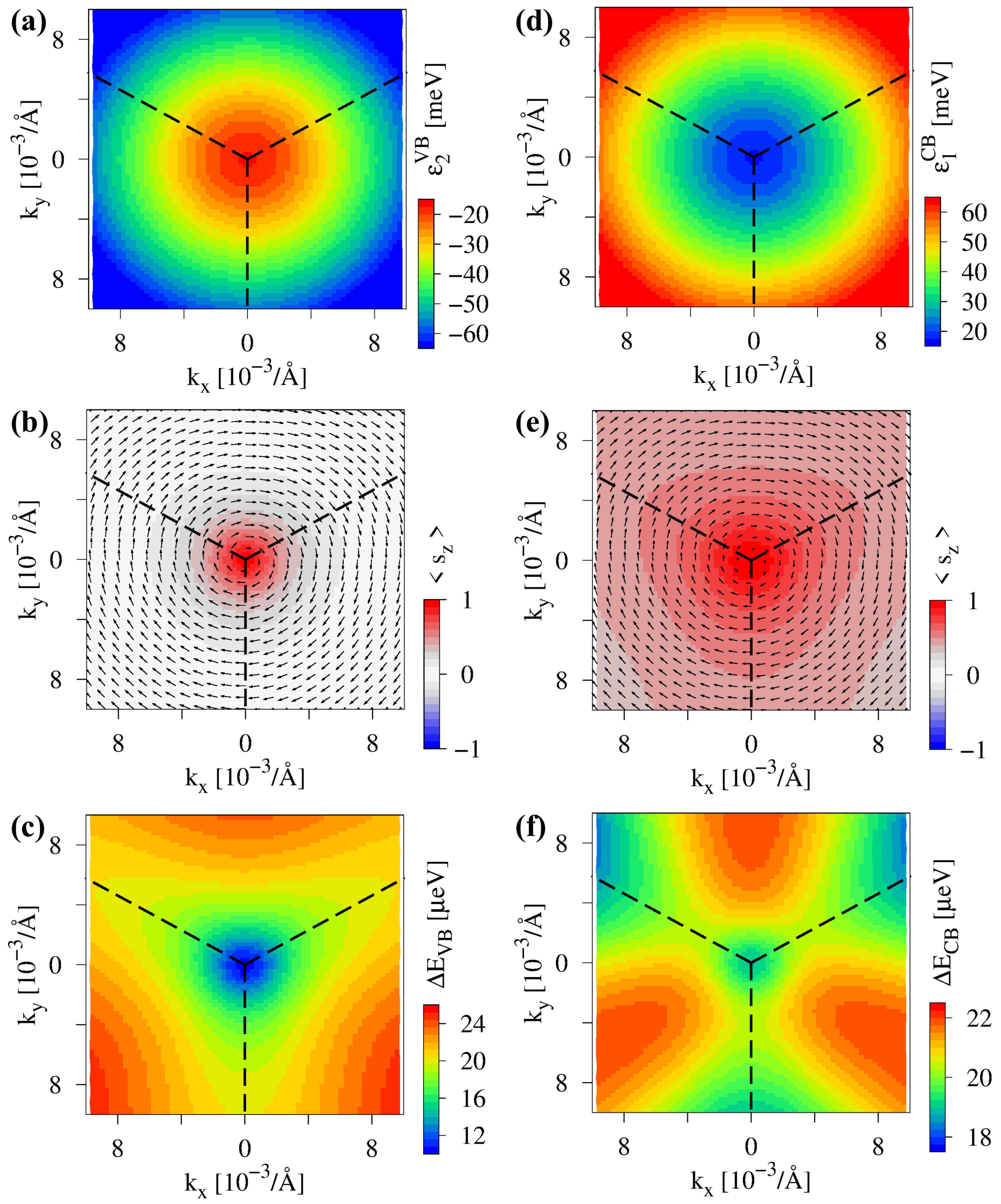 Figure 19
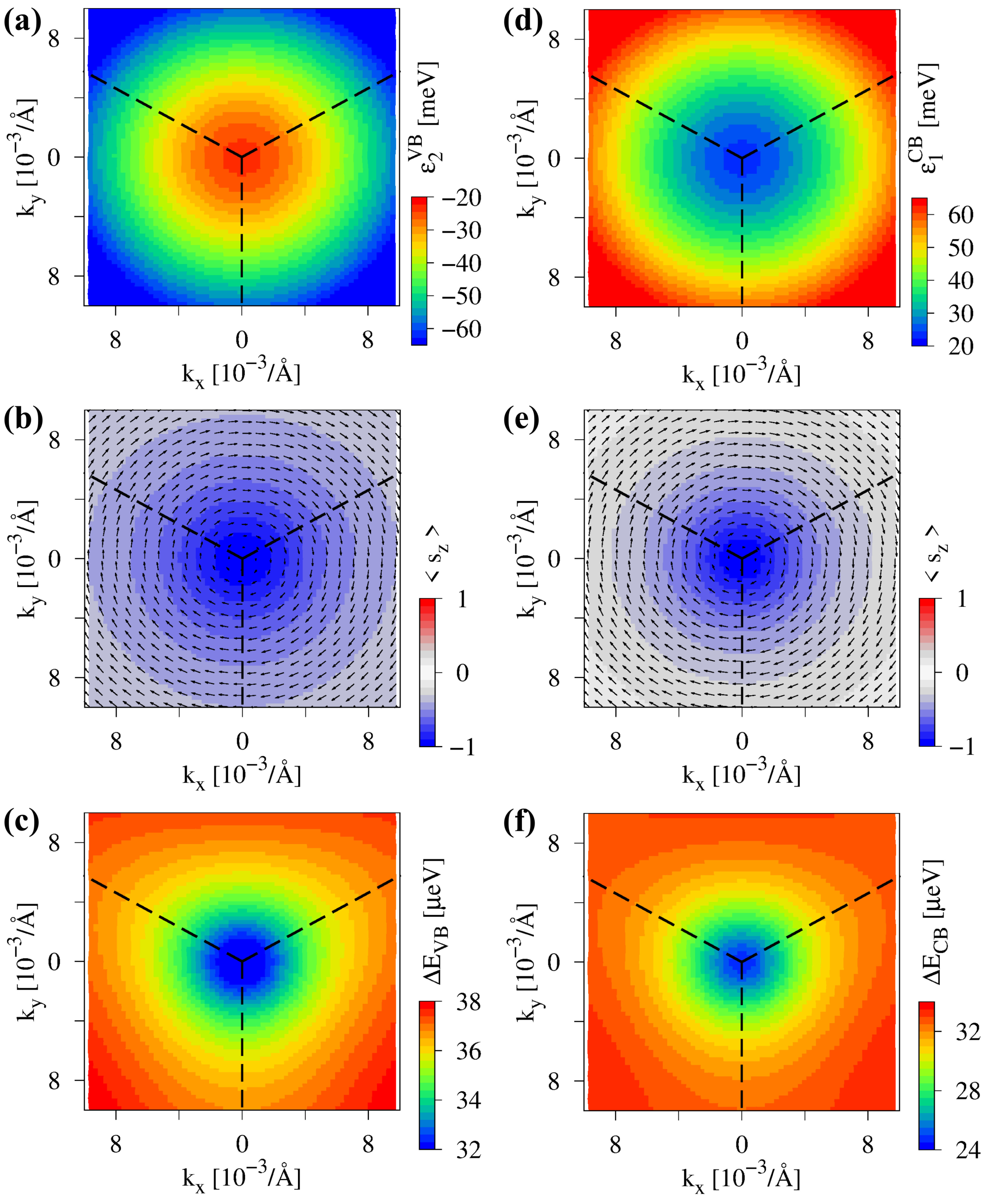 Figure 20
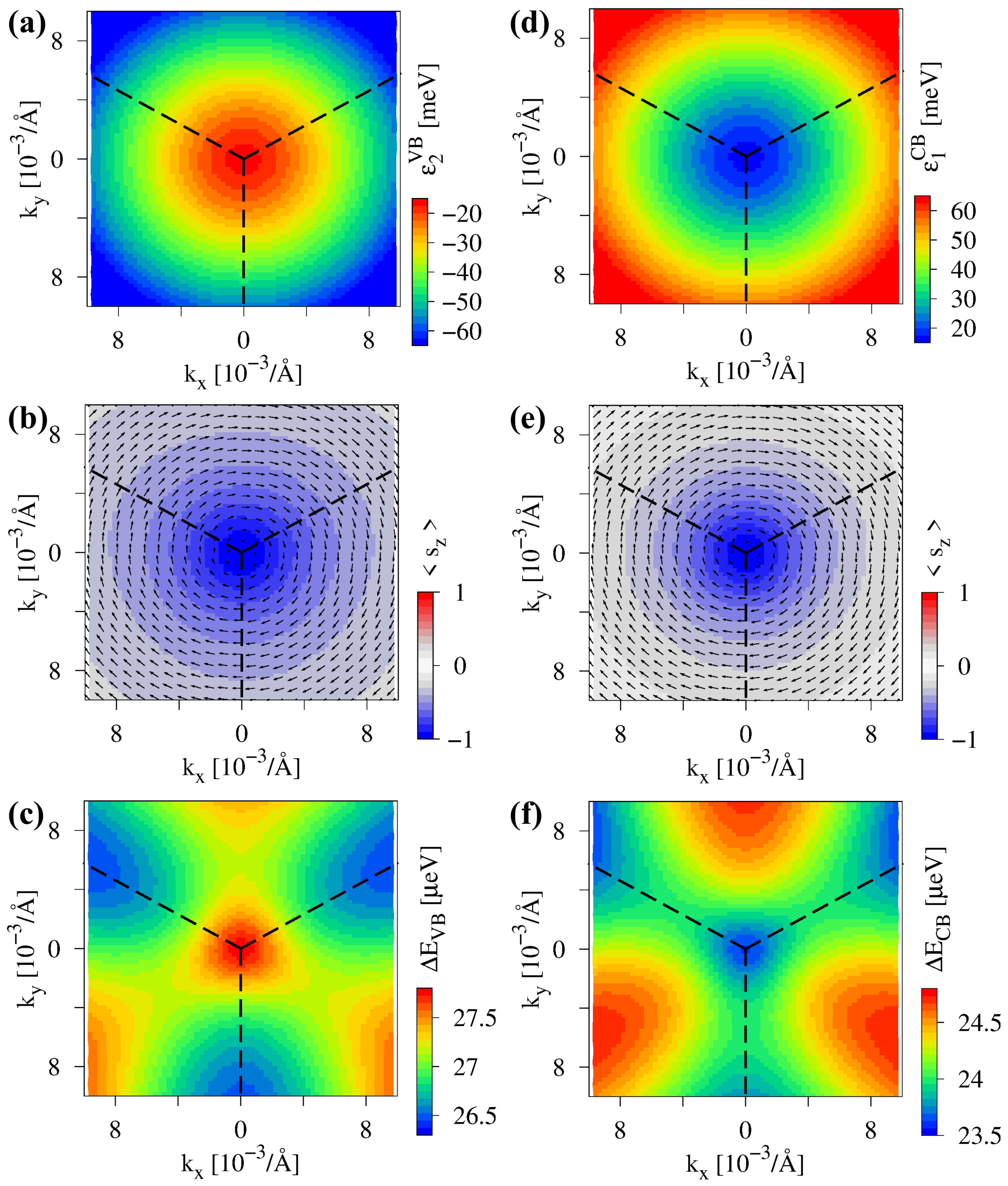 Figure 21
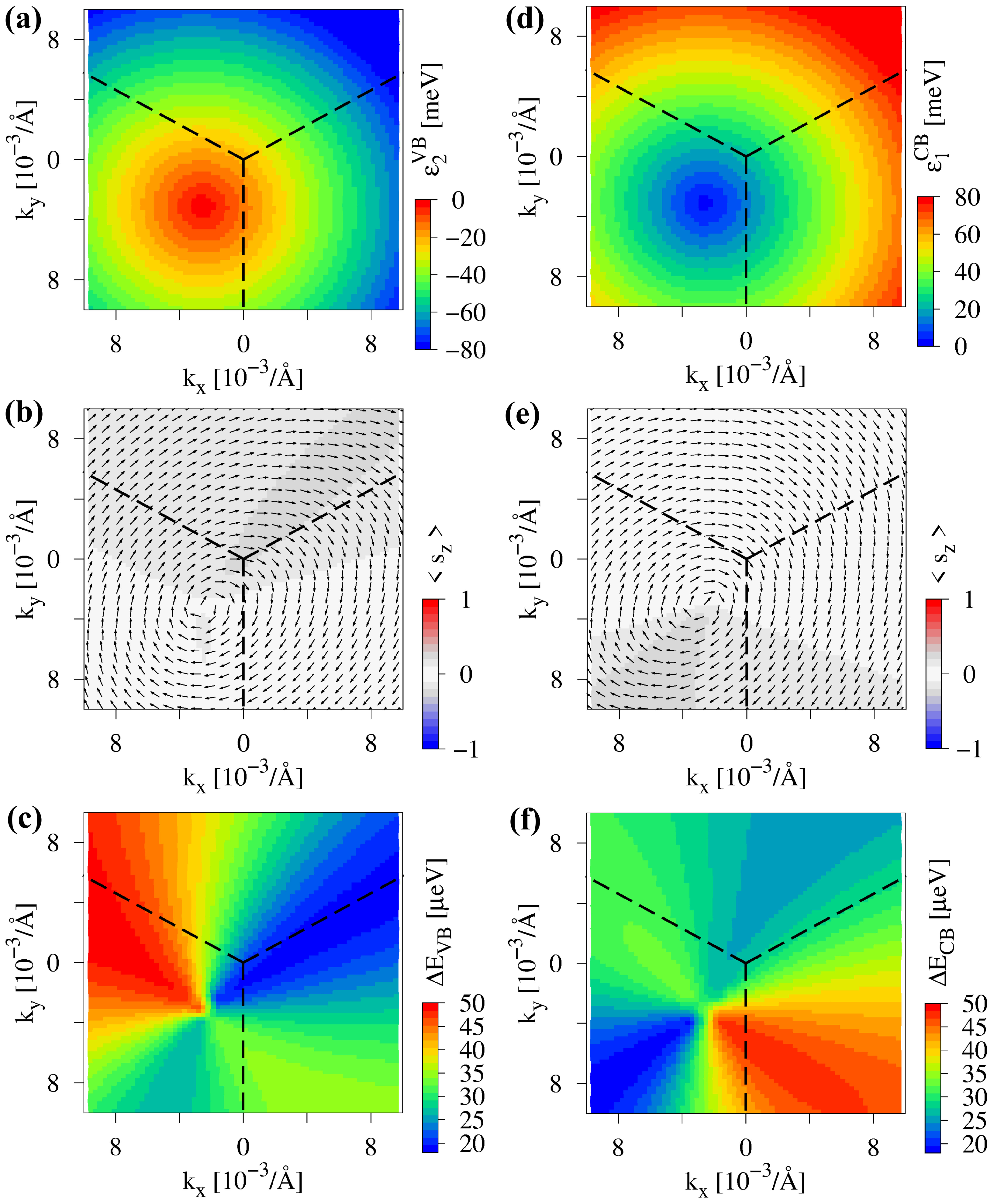 Figure 22
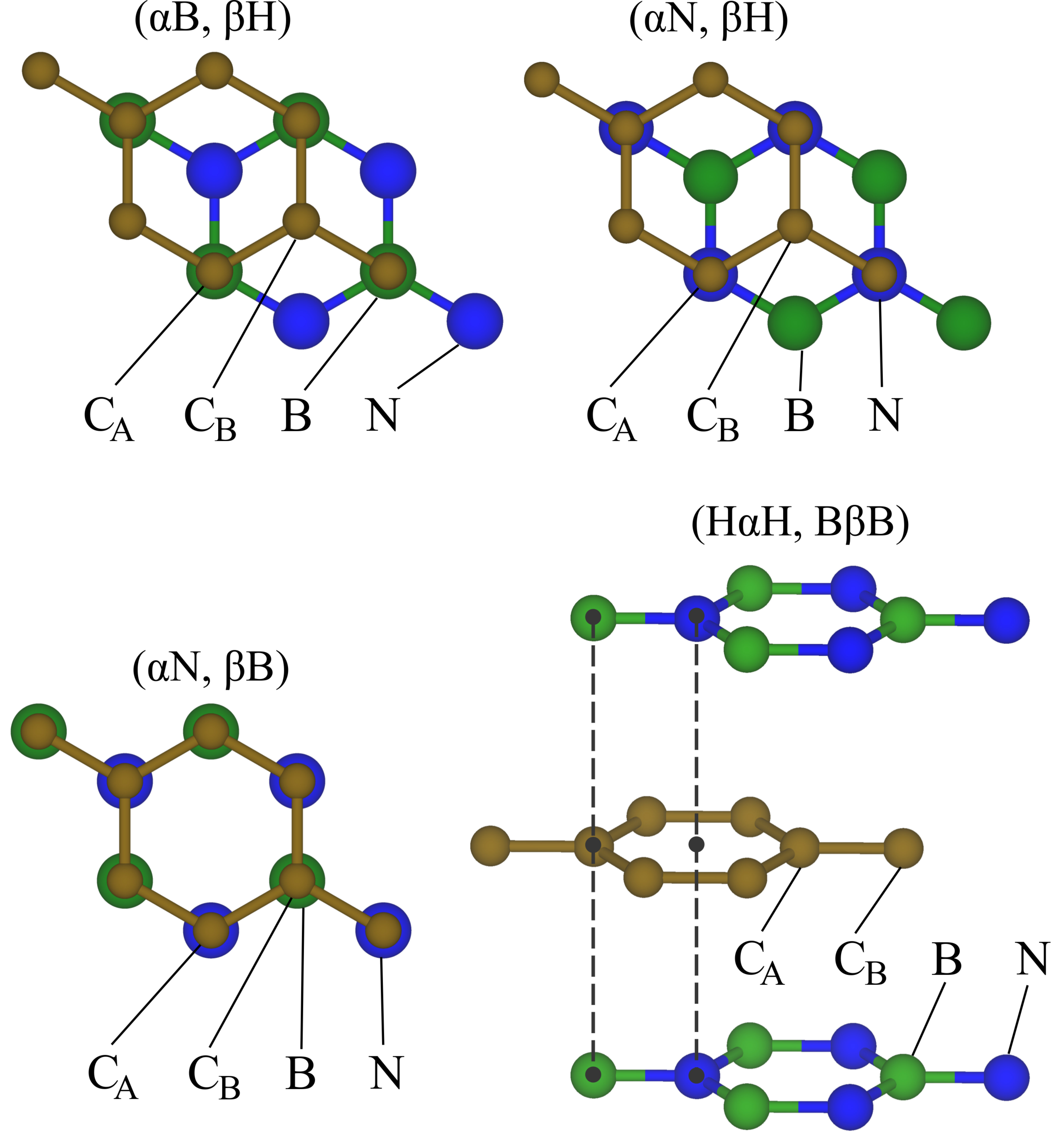 Figure 23
| Configuration | distance [Å] | [meV] | eV] | eV] | eV] | eV] | eV] | |
|---|---|---|---|---|---|---|---|---|
| (B, H) | 3.35 | 8.308 | -17.08 | 10.65 | 5.00 | 9.37 | 33.58 | 37.57 |
| (N, H) | 3.50 | 8.197 | 16.31 | 12.67 | 11.78 | 13.96 | 4.431 | 26.68 |
| (N, B) | 3.55 | 8.128 | 23.50 | 17.89 | 12.21 | 15.82 | 12.91 | 29.73 |
| average | 3.47 | 8.211 | 7.577 | 13.74 | 9.66 | 13.05 | 16.97 | 31.33 |
| SOC on | [meV] | eV] | eV] | eV] | eV] | eV] | discr. [a.u.] | |
|---|---|---|---|---|---|---|---|---|
| N, B, C | 8.308 | -17.08 | 10.65 | 5.00 | 9.37 | 33.58 | 37.57 | 1.265 |
| N, C | 8.308 | -17.08 | 12.22 | 5.01 | 8.95 | 34.65 | 34.82 | 1.269 |
| B, C | 8.308 | -17.08 | 10.23 | 12.08 | 12.66 | -0.06 | -34.82 | 0.260 |
| N, B | 8.308 | -17.07 | -1.82 | -7.09 | -2.79 | -9.53 | 66.55 | 1.349 |
| C | 8.308 | -17.07 | 11.85 | 12.07 | 12.25 | -4.60 | -32.67 | 0.268 |
| Configuration | [meV] | [meV] | eV] | eV] | eV] | eV] | eV] | |
|---|---|---|---|---|---|---|---|---|
| (HB, BH) | 0.01 | 8.296 | 0 | 0 | 2.19 | 2.19 | 0 | 0 |
| (HN, NH) | 26.60 | 8.068 | 0 | 0 | 13.31 | 13.31 | 0 | 0 |
| (NB, BN) | 32.05 | 7.931 | 0 | 0 | 15.76 | 15.76 | 0 | 0 |
| (HH, BB) = C1 | 0 | 8.294 | 34.24 | 0 | 6.65 | -2.05 | 0 | 0 |
| (NN, HH) | 26.09 | 8.070 | 34.10 | 0 | 11.38 | 15.47 | 0 | 0 |
| (BB, NN) | 31.76 | 7.932 | -48.00 | 0 | 18.95 | 12.34 | 0 | 0 |
| (HB, NH) | 13.12 | 8.175 | -34.85 | -1.97 | 6.51 | 9.05 | 3.15 | 31.35 |
| (NB, BH) | 15.89 | 8.110 | 6.29 | -7.75 | 5.09 | 12.84 | 1.26 | 22.72 |
| (BN, NH) | 29.20 | 7.998 | -6.50 | -4.97 | 15.23 | 13.92 | -61.34 | 49.22 |
| (NB, HH) | 13.16 | 8.176 | -0.069 | -2.58 | 4.76 | 11.01 | 16.02 | 15.98 |
| (BB, NH) | 15.85 | 8.108 | -41.50 | -7.37 | 8.31 | 9.55 | 6.71 | 16.36 |
| (NN, BH) | 28.82 | 8.000 | 41.14 | -3.29 | 11.89 | 17.26 | 94.83 | -106.79 |
| (HBN, BHH) | 0.07 | 8.296 | 0.093 | 0.40 | 2.06 | 2.22 | 0 | 0 |
| (BBN, HHH) | 0 | 8.298 | -34.06 | 0.31 | -2.23 | 6.66 | 0 | 0 |
Peer Reviews
No public reviews on file for this paper yet. If you reviewed it on a platform where reviews are public (OpenReview, ICLR, NeurIPS, ICML), you can paste yours below so the community can read it here.
Videos
No videos yet. Explain this paper in a talk, walkthrough, or lecture? Add one.
Heterostructures of graphene and hBN: electronic, spin-orbit, and spin relaxation properties from first principles
Klaus Zollner
Institute for Theoretical Physics, University of Regensburg, 93040 Regensburg, Germany
Martin Gmitra
Institute of Physics, P. J. Šafárik University in Košice, 04001 Košice, Slovakia
Jaroslav Fabian
Institute for Theoretical Physics, University of Regensburg, 93040 Regensburg, Germany
Abstract
We perform extensive first-principles calculations for heterostructures composed of monolayer graphene and hexagonal boron nitride (hBN). Employing a symmetry-derived minimal tight-binding model, we extract orbital and spin-orbit coupling (SOC) parameters for graphene on hBN, as well as for hBN encapsulated graphene. Our calculations show that the parameters depend on the specific stacking configuration of graphene on hBN. We also perform an interlayer distance study for the different graphene/hBN stacks to find the corresponding lowest energy distances. For very large interlayer distances, one can recover the pristine graphene properties, as we find from the dependence of the parameters on the interlayer distance. Furthermore, we find that orbital and SOC parameters, especially the Rashba one, depend strongly on an applied transverse electric field, giving a rich playground for spin physics. Armed with the model parameters, we employ the Dyakonov-Perel formalism to calculate the spin relaxation in graphene/hBN heterostructures. We find spin lifetimes in the nanosecond range, in agreement with recent measurements. The spin relaxation anisotropy, being the ratio of out-of-plane to in-plane spin lifetimes, is found to be giant close to the charge neutrality point, decreasing with increasing doping, and being highly tunable by an external transverse electric field. This is in contrast to bilayer graphene in which an external field saturates the spin relaxation anisotropy.
spintronics, graphene, heterostructures, proximity spin-orbit coupling
pacs:
72.80.Vp, 73.22.Pr, 71.70.Ej, 85.75.-d
I Introduction
Graphene encapsulated in hBN is emerging as the long-awaited platform for two-dimensional (2D) spintronics Han et al. (2014); Žutić et al. (2004). First generation graphene devices, based on SiO2/Si substrates Han et al. (2010); Popinciuc et al. (2009); Han and Kawakami (2011); Han et al. (2012); Fan et al. (2012); Gao et al. (2014); Kang et al. (2008); Wang et al. (2013); Maassen et al. (2011); Yang et al. (2011); Tombros et al. (2007), show very poor spin transport and ultrafast spin relaxation (SR) with spin lifetimes of a few hundred picoseconds. In contrast, theory predicts only a few eV SOC in pristine graphene Gmitra et al. (2009); Boettger and Trickey (2007); Konschuh et al. (2010) and outstanding spin lifetimes in the nanosecond range Ertler et al. (2009); Pesin and MacDonald (2012); Min et al. (2006); Dugaev et al. (2011); Huertas-Hernando et al. (2009). However, due to electron-hole puddles Van Tuan et al. (2016); Martin et al. (2008), surface roughness, defects and impurities Sabio et al. (2008); Chen et al. (2008) originating from the substrate, graphene’s SOC can be significantly increased, substantially influencing electronic and spin transport properties. Furthermore, the absence of a marked SR anisotropy in these devices Raes et al. (2016); Ringer et al. (2018); Zhu and Kawakami (2018) was explained by the presence of magnetic resonant scatterers Irmer et al. (2018); Kochan et al. (2014); Miranda et al. (2017). One attempt of counteracting the substrate’s influence is to suspend graphene Guimarães et al. (2012); Du et al. (2008); Bao et al. (2009), yielding high mobilities but also limited spin transport. Therefore the search for new substrates revealed that hBN is the material of interest.
The new generation of graphene devices is based on (hBN)/graphene/hBN stacks Roche et al. (2015); Kamalakar et al. (2014); Gurram et al. (2018a); Guimarães et al. (2014); Singh et al. (2016); Drögeler et al. (2016, 2017); Zomer et al. (2012); Ingla-Aynés et al. (2015); Drögeler et al. (2014); Dean et al. (2012, 2010); Wang et al. (2017a), which have outstanding transport properties with giant mobilities up to 106 cm2/Vs Banszerus et al. (2015); Petrone et al. (2012); Calado et al. (2014) and record spin lifetimes exceeding 10 ns Drögeler et al. (2016). Owing to the improved growth techniques, large scale, defect free, and smooth interfaces of graphene and hBN Xue et al. (2011); Van Tuan et al. (2016); Mishra et al. (2016); Tang et al. (2013); Arjmandi-Tash et al. (2018); Zomer et al. (2011) can be easily produced. Especially this second generation of graphene devices is very important for the realization of spintronics and spin-logic devices Gurram et al. (2016); Mayorov et al. (2011); Gurram et al. (2017, 2018b, 2018a); Han et al. (2014); Kamalakar et al. (2014); Britnell et al. (2012); Wang et al. (2017b); Fabian et al. (2007); Žutić et al. (2004); Lin et al. (2013, 2014); Luo et al. (2017); Wen et al. (2016); Zutic et al. (2006); Behin-Aein et al. (2010).
There is now experimental evidence that in hBN encapsulated bilayer graphene, SR is due to SOC Leutenantsmeyer et al. (2018); Xu et al. (2018). Finally there is a graphene-based structure in which spins live long (10 ns) and SOC is strong enough, relative to other spin-dependent interactions, to play a dominant role and be used for spin manipulation. The evidence comes from SR anisotropy. In 2D electron gases in semiconductor quantum wells the out-of-plane electron spins have lifetimes () smaller than in-plane spins (), due to the in-plane Rashba fields Žutić et al. (2004). Typically the SR anisotropy ratio is 0.5, reflecting the fact that two spin-orbit field components can flip an out-of-plane spin, but only one component can flip the in-plane spin. In contrast, as recently predicted Cummings et al. (2017) and soon experimentally realized Leutenantsmeyer et al. (2018); Xu et al. (2018); Zihlmann et al. (2018); Omar and van Wees (2018), 2D materials offer so far unrivaled control over . It was found that graphene on a transition metal dichalcogenide (TMDC) has , due to the strong valley Zeeman spin-orbit fields, being induced from the TMDC into graphene. In this system the spin-orbit fields are relatively large (1 meV Gmitra et al. (2016)) compared to graphene (10 eV Gmitra et al. (2009)), which is also reflected in the rather small spin lifetimes of about 10 ps.
On the other hand, the SR anisotropy in encapsulated bilayer graphene is also giant (), but the spin lifetime is three orders of magnitude larger, up to 10 ns Leutenantsmeyer et al. (2018); Xu et al. (2018). Remarkably, the SR anisotropy sharply increases as a transverse electric field is applied Xu et al. (2018) at a fixed doping. This is counterintuitive, since the applied field should increase the Rashba field and lower . The resolution lies in the idiosyncratic spin-orbit band structure of bilayer graphene. In the presence of even a moderate electric field, the lowest energy bands at K split due to SOC, but the splitting does not depend on the field, acquiring the intrinsic value of about 24 eV Konschuh et al. (2012), determined by density-functional theory (DFT).
Since SR anisotropy in mono- and bilayer graphene has been a hotly debated issue recently, we ask the following questions. What are the spin lifetime limits in (hBN)/graphene/hBN heterostructures? Does monolayer graphene also have a large SR anisotropy, as shown in hBN encapsulated bilayer graphene? Can the anisotropy be tuned electrically?
Here we focus on monolayer graphene encapsulated in hBN, or placed on a hBN substrate. We predict, by DFT calculations and phenomenological modeling, the values of induced spin-orbit fields, as well as what is the expected SR anisotropy in a variety of potentially realizable structures. It is shown (and this should be true for bilayer graphene at low electric fields as well) that the anisotropy depends on the actual atomic arrangement of the structures and is highly electrically tunable. Unlike in bilayer graphene, in our systems the anisotropy decreases with increasing electric field, being giant (about 10) at low fields and reaching the Rashba limit of 50% at large fields. The spin lifetimes are expected to be on the order of 10 ns, as already seen experimentally, and also theoretically elaborated for SOC in the tens of eV range Van Tuan et al. (2016).
II Geometry & Computational Details
In order to calculate the electronic band structure of (hBN)/graphene/hBN heterostructures, we use a common unit cell for graphene and hBN. Therefore, we fix the lattice constant of graphene Castro Neto et al. (2009) to Å and change the hBN lattice constant from its experimental value Catellani et al. (1987) of Å to the graphene one. The lattice constants of graphene and hBN differ by less than 2%, justifying our theoretical considerations of commensurate geometries. While the small lattice mismatch does lead to moiré patterns Jung et al. (2014); Moon and Koshino (2014); Argentero et al. (2017), the global band structure of local individual stacking configurations is qualitatively similar Quhe et al. (2012); Giovannetti et al. (2007). Nevertheless, here we consider all structural arrangements for commensurate unit cells, so as to get a quantitative feeling for spin-orbit phenomena in a generic experimental setting.
The stacking of graphene on hBN is a crucial point, however it was already shown that the configuration with the lowest energy is, when one C atom is over the B atom and the other C atom is over the hollow site of hBN Giovannetti et al. (2007). Before we proceed, we define a terminology to make sense of the structural arrangements, used in the following. We denote the three relevant sites in hBN as the B site (boron), the N site (nitrogen), and the H site (hollow position in the center of the hexagon). Similarly, we have two graphene sublattices (C) and (C). We call the energetically most favorable configuration (B, H), where C is over Boron, and C is over the hollow site. According to this definition we define the other configurations as (N, H) and (N, B). Due to symmetry, the configurations with interchanged C and C sublattices give the same results. The lowest energy interlayer distances between graphene and hBN are different for the different stackings Giovannetti et al. (2007). We include a distance study for all three configurations, in order to reveal what are the corresponding lowest energy distances.
In analogy, a stacking sequence of hBN encapsulated graphene is then abbreviated as (UV, XY), indicating that the () sublattice of graphene is sandwiched between the U and V (X and Y) sites of top and bottom hBN, each of which can take the values {B, N, H}. It has been shown Quhe et al. (2012), that the energetically most favorable sandwich structure is (HH, BB) in agreement with our findings here, meaning that () is sandwiched between the two H sites (B sites) of top and bottom hBN. Interlayer distances, used in the encapsulated geometries, are the ones determined by the distance study of the nonencapsulated structures. In Fig. 1 we show the three commensurate stacking configurations of graphene on hBN, as well as the (HH, BB) geometry, as an example of hBN encapsulated graphene.
First-principles calculations are performed with full potential linearized augmented plane wave (FLAPW) code based on DFT Hohenberg and Kohn (1964) and implemented in WIEN2k Blaha et al. (2001). Exchange-correlation effects are treated with the generalized-gradient approximation (GGA) Perdew et al. (1996), including dispersion correction Grimme et al. (2010) and using a -point grid of in the hexagonal Brillouin zone if not specified otherwise. The values of the muffin-tin radii we use are for C atom, for B atom, and for N atom. We use the plane wave cutoff parameter . In order to avoid interactions between periodic images of our slab geometry, we add a vacuum of at least Å in the direction.
III Model Hamiltonian & Full Band Structure
The band structure of proximitized graphene can be modeled by symmetry-derived Hamiltonians Kochan et al. (2017). For (hBN)/graphene/hBN heterostructures having symmetry, the effective low energy Hamiltonian is
[TABLE]
Here is the Fermi velocity and the in-plane wave vector components and are measured from K, corresponding to the valley index . The Pauli spin matrices are , acting on spin space (), and are pseudospin matrices, acting on sublattice space (C, C), with and . The lattice constant is Å of pristine graphene and the staggered potential gap is . The parameters and describe the sublattice resolved intrinsic SOC, stands for the Rashba SOC, and and are the sublattice resolved pseudospin-inversion asymmetry (PIA) SOC parameters. The basis states are , , , and , resulting in four eigenvalues .
The calculated band structure of encapsulated graphene in the (HH, BB) configuration is shown in Fig. 2, as a representative example for all considered geometries. Other stacking geometries, as well as graphene on hBN, exhibit similar band features. The Dirac bands of graphene are located within the hBN band gap. In general, the geometries we consider in the following, have broken pseudospin symmetry, and a band gap opens in graphene. Then, e.g., C orbitals form the conduction band (CB), while C ones form the valence band (VB). Further, the low energy bands split into four states due to SOC and the Rashba effect, see left inset in Fig. 2. The general strategy is now to calculate the low energy bands and extract the model Hamiltonian parameters best fitting the DFT results, for all (hBN)/graphene/hBN geometries.
IV Graphene on hBN
In this section we discuss the graphene/hBN heterostructures. We show our fit results to the low energy Hamiltonian for the different stacking configurations and analyze the influence of the interlayer distance, between graphene and hBN, on the extracted orbital and SOC model parameters. Furthermore, we show and discuss calculated spin-orbit fields. Before we turn to the calculation of the SR properties, we show the tunability of the parameters by applying a transverse electric field for one specific stacking configuration. Finally, we discuss the accuracy of the model, analyze atomic SOC contributions and consider an arbitrary but special graphene/hBN stack.
IV.1 Low energy bands
In Fig. 3 we show the calculated low energy band structure in the vicinity of the K point with a fit to our minimal tight-binding Hamiltonian for the (B, H) configuration of graphene on hBN. We can see that the orbital band structure is perfectly reproduced by our model, see Fig. 3(a), in a quite large energy window around the Fermi level. The splittings of the bands are shown in Fig. 3(b), which are in the eV range and are defined as and . Also the splittings are nicely reproduced by the model, with a maximum discrepancy of about 10% compared to the first-principles data. More specifically, the splittings are overestimated (underestimated) along the K-M (K-) path, by the model. The reason for the discrepancy of the fit will be explained at a later point. Finally, Figs. 3(c)-3(e) show the spin expectation values of the bands and , which are in perfect agreement with the model. The and spin expectation values show a pronounced signature of Rashba SOC, with a sign change around the K point. The expectation values are maximum at the K point, slowly decaying away from it.
In Figs. 4 and 5 we show the fits to the model Hamiltonian for the (N, H) and (N, B) configurations. The overall results look similar to the (B, H) configuration. The orbital band structure, splittings, and spin expectation values are again nicely reproduced by the model. Compared to the (B, H) case, band splittings are even better reproduced in these two cases, with a maximum discrepancy of 3% and 1%, respectively. The and spin expectation values again show the characteristic signature of Rashba SOC, originating from the broken inversion symmetry of graphene, due to the hBN substrate. However, the expectation values, also decaying away from K, are opposite compared to the (B, H) case. We find that our model is very robust and different stacking configurations are described by different parameter sets. The extracted parameters are given in Tab. 1 for the three commensurate high-symmetry graphene/hBN stacking configurations, with their corresponding lowest energy distance.
IV.2 Distance study
One has to mention that different stacking configurations lead to different interlayer distances between graphene and hBN, when minimizing the total energy of the individual geometries. In Fig. 6 we show the fit parameters, as a function of the distance between graphene and hBN, for the three stacking configurations. We find that the total energy is lowest for the (B, H) configuration with an interlayer distance of Å, see Fig. 6(a). The lowest energies for the (N, H) and (N, B) configurations are obtained at distances of Å and Å. The Fermi velocity , see Fig. 6(b), which reflects the nearest neighbor hopping strength via , grows as a function of distance, especially for the (N, H) and (N, B) configurations. In contrast to that, the gap parameter decreases with distance, in agreement with literature Giovannetti et al. (2007). When moving the graphene away from the substrate, the sublattice symmetry breaking reduces and the gap decreases.
One very important observation is that the gap parameter of the (B, H) configuration is opposite in sign compared to the other configurations, as seen in a moiré pattern Miller et al. (2010); Hunt et al. (2013); Kindermann et al. (2012). In the (B, H) configuration, the C sublattice is over the boron. Sublattice C forms, in this case, the VB which is why we need a negative value of in the model, to match the sublattice character of the DFT results. In contrast, the other configurations have the C sublattice over the nitrogen, which then forms the CB, leading to a positive value of . This also explains why the spin expectation values for different configurations are different, compare Figs. 3(e) and 4(e). In a moiré pattern geometry, with micrometer size flakes of graphene and hBN, all of these local stacking configurations appear simultaneously. Consequently, there can be a local stacking geometry where the orbital gap closes, appearing when the two sublattices feel the same surrounding potential. We will calculate and discuss such a situation at a later point, for a certain choice of stacking.
The Rashba SOC parameter, see Fig. 6(d), also decreases with distance. When the distance between graphene and hBN approaches infinity, the inversion symmetry of graphene is restored and the Rashba SOC parameter vanishes. The two intrinsic SOC parameters and approach the intrinsic SOC of eV of pristine graphene Gmitra et al. (2009), as we increase the distance, see Figs. 6(e) and 6(f). Finally, we find that the two PIA SOC parameters and , see Figs. 6(g) and 6(h), also decrease with distance. Overall, as expected, we restore the pristine graphene properties, as the interlayer distance gradually increases.
IV.3 Spin-Orbit fields
In Fig. 7 we show the calculated dispersion as a 2D map in - plane in the vicinity of the K point for the (B, H) configuration. The energies of the bands, and , do not show any trigonal warping, see Figs. 7(a) and 7(d). However, already the spin texture shows that trigonal warping is present with a very pronounced Rashba spin-orbit field, rotating in a clockwise direction, see Figs. 7(b) and 7(e), as expected from the inversion symmetry breaking by the hBN substrate. In contrast to the CB, the VB spin expectation value strongly decays away from the K point. A pronounced threefold symmetry is observed in the spin splittings and , see Figs. 7(c) and 7(f). Along the K- path, the Dirac bands are more split than along the K-M path. As we have seen, our model Hamiltonian agrees very well on a qualitative level for this case, see Fig. 3, however the band splittings cannot be fully recovered. The reason will be explained in the last subsection. In Figs. 8 and 9 we show the calculated dispersion as a 2D map in the - plane in the vicinity of the K point for the (N, H) and (N, B) configurations. The overall trigonal symmetry features remain and are very similar to the (B, H) configuration. Especially for the (N, B) configuration, only weak trigonal symmetry, around the K point, can be observed.
IV.4 Transverse electric field
In experiment gating is required to tune the Fermi level towards the charge neutrality point. By using top and back gate electrodes, one can tune the doping level and simultaneously apply an electric field across a heterostructure. Thereby the transverse electric field can influence electronic and spin-orbit properties of graphene, especially the Rashba SOC Gmitra et al. (2009). We consider the lowest energy configuration (B, H) for graphene on hBN and apply a transverse electric field, which is modeled by a zigzag potential, across the heterostructure.
For every magnitude of the field we calculate the low energy band structure and fit it to the model Hamiltonian. In Fig. 10 we show the fit parameters for (B, H) configuration as a function of external electric field. Indeed, we can tune most of the parameters. The Fermi velocity , as well as intrinsic SOC parameters and , are barely affected. However, the field can tune the orbital gap, Rashba and PIA SOC parameters. Especially the Rashba parameter can be tuned over a wide range, even from positive to negative values, with the transition at around 2 V/nm. Tuning the Rashba SOC parameter, from a positive to a negative value, also allows us to change the rotation direction of the spin-orbit fields, see Figs. 7(b) and 7(e). Most importantly we can tune the Rashba SOC from a finite value to zero. Consequently, we can control the strength of the in-plane spin-orbit field, dictated by Rashba SOC, which will significantly influence spin transport and SR properties. Another feature we notice is that around 2 V/nm, the PIA SOC parameters are not changing very smoothly with applied field, which is connected with the transition of the Rashba SOC through zero.
IV.5 Spin relaxation anisotropy
Since the low energy Hamiltonian can nicely reproduce the dispersion around the K point, we can use it together with our fit parameters to calculate SR times. We calculate, for a very dense grid in the vicinity of the K point, the energy spectrum and spin expectation values for the Dirac bands from our model. To calculate the SR time, we define the spin-orbit field components as Fabian et al. (2007)
[TABLE]
where is the momentum and are the spin expectation values along the direction . The energy splitting of the Dirac bands is and is the absolute value of the spin. By that we obtain at each point the spin-orbit vector field. Following the derivation of Refs. Cummings et al., 2017; Garcia et al., 2018, we then calculate the SR times as follows
[TABLE]
The average is taken over all points that have the same constant energy . The momentum relaxation time is and is the intervalley scattering time. For the calculation of the averages we use energy steps of eV with a smearing of eV, corresponding to a temperature of K. Measurements Drögeler et al. (2016); Gurram et al. (2018a); Guimarães et al. (2014); Singh et al. (2016) provide SR lengths of m, SR times of ns, and spin diffusion constants of . With the relation and using that the spin diffusion constant is roughly equal to the charge diffusion constant and , we get fs, which we use in the calculations. The value for is reasonable, assuming ultraclean samples.
Since intervalley scattering times are hard to estimate from experiments, we consider it variable, with , for our calculations. By that we obtain the SR time as a function of the energy, for spins along the , , and direction for each ratio . More interesting than the individual SR times is the SR anisotropy , a measurable fingerprint of the SOC of the system.
We show a colormap of the calculated anisotropy as a function of and the energy for the (B, H) configuration in Fig. 11(a). Within the band gap of meV, of course no states are available and SR times cannot be calculated, because the smearing we use is only K. For holes we find that the anisotropy is , the Rashba limit, as soon as we are below meV from the valence band edge, for each ratio . For electrons the situation is completely different and the anisotropy can get very large, even meV away from the conduction band edge. We also find that, independent of , the anisotropy is largest close to the band edges, which would correspond to the charge neutrality point in experiment. In Fig. 11(b) we show the individual SR times as a function of energy, corresponding to . We find SR times of around 10 ns, consistent with measurements Drögeler et al. (2016). However, we have to keep in mind that Fig. 11 is only valid for a certain stacking configuration, the (B, H) one, of graphene on hBN.
In experiment one expects, that electrons traveling through graphene on a hBN substrate would rather experience local spin-orbit fields that can be very different for certain regions due to the different stacking configurations. Therefore, in Fig. 12(a) we show a colormap of the calculated anisotropy as a function of and the energy when using the averaged parameters of graphene on hBN given in Tab. 1. This averaged situation should correspond to a more realistic situation in a real heterostructure, where all kinds of stacking configurations are present simultaneously. We find that electrons have an anisotropy ratio almost independent of and the energy, see Fig. 12(b), clearly different from the pure (B, H) configuration, compare to Fig. 11. Close to the band edges, i.e. the charge neutrality point, the anisotropy can reach very large values. For holes the anisotropy varies around for moderate doping densities.
So far, anisotropies of have been measured for graphene on hBN and SiO2 Guimarães et al. (2014); Raes et al. (2017, 2016); Ringer et al. (2018); Tombros et al. (2008), in agreement with our averaged parameter results. A first indication of large anisotropies was found in hBN encapsulated bilayer graphene heterostructures Leutenantsmeyer et al. (2018); Xu et al. (2018). There it was shown, that the anisotropy decreases with increasing carrier density, in line with our results for monolayer graphene. They also showed that the anisotropy, at fixed doping level, can be strongly enhanced by an applied electric field.
In dual gated structures, one can individually tune the doping level and the electric field across the heterostructure. In Fig. 13 we show the SR anisotropy , specifically for (B, H) configuration as a function of energy and applied transverse electric field, using the parameter sets for several finite electric field strengths, see Fig. 10. We find that the anisotropy is strongly tunable by means of external gating. At around 2 V/nm we find a very strong enhancement of the anisotropy, which is related to the zero transition of the Rashba SOC parameter. The anisotropy is giant for , as the states are then mainly polarized. In Fig. 13(b) we show that an electric field can tune the anisotropy by one order of magnitude at a fixed doping level.
IV.6 Additional considerations
We now want to clarify two remaining issues: (i) Where does the discrepancy between the model and the first-principles data, see Fig. 3(b), come from? (ii) Is there a low-symmetry stacking configuration, where the orbital gap closes?
IV.6.1 Model Discrepancy
In the case of the (B, H) configuration, we have found that the splittings are overestimated (underestimated) along the K-M (K-) path, by the model. The discrepancy in the splitting of the bands is due to the influence of the substrate. In general, the model Hamiltonian just considers effective orbitals of graphene, however there seems to be a subtle influence from a hybridization to the orbitals of hBN. If we look at the density of states (DOS) for the (B, H) case, see Fig. 14, we find that close to the Dirac point there is a small contribution from nitrogen and boron states. Especially boron orbitals and nitrogen orbitals are contributing close to the charge neutrality point. Moreover, from our distance study we find that the discrepancy between the model and the first-principles data is getting smaller as we increase the interlayer distance.
Finally, we calculate the low energy band structures, when SOC is artificially turned off on the nitrogen, boron, or carbon atoms, respectively. The fit parameters for these situations are given in Tab. 2, along with the maximum discrepancy for each situation. When SOC of the boron atom is turned off, the parameters and the fit accuracy are barely different. A severe improvement of the fit is accomplished, when SOC of the nitrogen atom is turned off, reflected in the strongly reduced discrepancy between model and DFT data. Furthermore, if we turn off SOC on the carbon atoms of graphene, we can identify the contribution solely coming from the substrate, where we find negative intrinsic SOC parameters and . Thus, nitrogen gives a non-negligible contribution to the SOC splitting of the Dirac bands.
From our analysis, we conclude that the discrepancy comes from nitrogen orbitals, that hybridize with orbitals of graphene. Already such a very small contribution of orbitals, see Fig. 14(a), can substantially influence the spin splitting and an effective model, based only on orbitals of graphene, can no longer perfectly describe the results. However, the overall fit is still very good and sufficient for our needs.
IV.6.2 Gap closing stacking
We have seen that different stackings can lead to a different sign of the gap parameter , see Tab. 1. Consequently, as already mentioned, a local stacking geometry can exist, in a real moiré pattern geometry, that has a closed orbital gap. In Fig. 15 we show the low energy band properties of an arbitrary stacking geometry, without having any symmetry 111The stacking is chosen such that each graphene sublattice has the same distance to an underlying boron and nitrogen atom. This seemed to be a good candidate for a gap closing, as the difference in the sublattice potential could vanish..
First of all, we notice that the Dirac point is no longer located at the K point. From the corresponding geometry in Fig. 15(a), we find that the hoppings, from say to the three nearest neighbors , are all different due to the substrate. This asymmetry in the nearest neighbor hopping amplitudes leads to the shift of the Dirac point in momentum space Pereira et al. (2009); Wunsch et al. (2008). Since our model Hamiltonian considers only high-symmetry stacking configurations, without shifted Dirac cone, we cannot fit the data with it. From the spin expectation values we find a very pronounced Rashba spin-orbit field, as the component is strongly suppressed.
In order to identify the location of the Dirac point in momentum space, we calculate the dispersion as a 2D map in - plane in the vicinity of the K point, see Fig. 16. Indeed, we find that the Dirac point is shifted away from the corner of the Brillouin zone. At the Dirac point, the orbital gap is meV large. Due to the limited number of points in the calculation grid for the 2D map, we cannot identify the exact position of the Dirac point, so the orbital gap is not fully closed, but much smaller than in the high-symmetry stacking cases, see Tab. 1. We also notice that the spin-orbit field is almost purely in-plane without any component, see Figs. 16(b) and 16(e), in a very large area around the Dirac point. Consequently, Rashba SOC plays an important role in this low-symmetry stacking configuration. If we look at the spin-orbit splitting of the bands, Figs. 16(c) and 16(f), we find that there is no trigonal symmetry remaining. Such a stacking configuration completely breaks the symmetry of the graphene, due to the different hopping amplitudes between nearest neighbors caused by the hBN substrate. Of course, in a moiré geometry, several other stackings are present, that lead to very different local orbital gaps, spin-orbit fields, and spin splittings.
V hBN encapsulated graphene
In this section we discuss the hBN/graphene/hBN heterostructures. We show our fit results to the low energy Hamiltonian for the different stacking configurations. Compared to the previous section, symmetry plays an important role when fitting the Hamiltonian. Again, we show the tunability of the parameters by applying a transverse electric field across the heterostructures. Finally we calculate SR times and anisotropies, and highlight differences to experimental findings in bilayer graphene.
V.1 Low energy bands
From our previous study of graphene on hBN, we already know what is the energetically most favorable distance for each stacking geometry, which we keep for the encapsulated cases, respectively. Depending on the stacking of the top and bottom hBN with respect to the graphene, different interlayer distances can be present. The stacking sequences are defined in analogy to the graphene on hBN cases. The energetically most favorable configuration is (HH, BB), which we name C1 configuration. According to this, we define several other configurations.
For such a configuration, like (HH, BB) = C1, we recover the mirror symmetry of graphene, see Fig.1, reflected in the symmetric version of the Hamiltonian with vanishing Rashba and PIA contributions Kochan et al. (2017). In Fig. 17, we show the low energy band properties of the C1 configuration, along with a fit to our model Hamiltonian. We can see perfect agreement with the first-principles data, just using the four parameters , , , and . Rashba and PIA SOC parameters are not necessary and strictly zero for the fit, especially for this mirror symmetric configuration, as explained. Therefore the bands are purely polarized.
In Figs. 18 and 19, we show the low energy band properties of the (BN, NH) and (NN, BH) configurations, along with a fit to our model Hamiltonian, as further examples of the robustness of the Hamiltonian. We can see again perfect agreement with the first-principles data. Even though the low energy band properties are somewhat similar, each configuration has a very individual parameter set.
The parameters, best fitting the DFT results, are given in Tab. 3. We find that there is another configuration, (HB, BH), having almost the same total energy as the (HH, BB) one, in agreement with literature Quhe et al. (2012). Overall, the magnitudes of SOCs are tens of eV, while the parameters can differ (also in sign) from structure to structure. For example, the (HB, BH) configuration is in the subgroup and the only allowed SOC parameters are . In this case the orbital gap , since the overall potential, from top and bottom hBN layer, is equal for the two graphene sublattices. When , the spectrum opens a gap due to SOC with degenerate CB and VB, just as for pristine graphene Gmitra et al. (2009). Also worth noticing is, that if one takes the average of and of the C1 configuration, you arrive at the parameter for the (HB, BH) configuration. In addition, some encapsulated configurations show a negative Rashba SOC parameter. This means that the spin-orbit field rotates in a counterclockwise direction, in contrast to the graphene/hBN cases, see for example Fig. 7.
In real systems, one expects that all of these configurations are present at the same time, due to the moiré pattern that is formed as a consequence of slightly different lattice constants of graphene and hBN. In addition stacking configurations can occur that, locally, have no symmetry at all, as shown in the previous section, making these heterostructures quite complicated to describe on the global scale. In experiments, also asymmetric hBN encapsulated graphene structures are used, say with two hBN layers below graphene and one hBN layer above it. We also calculate this scenario, especially for the configurations that are energetically most favorable. The stacking of hBN itself is (BN, NB) (boron over nitrogen, nitrogen over boron) and we take a distance of Å between the hBN layers. These configurations and their fit parameters are also summarized in Tab. 3, with the naming convention in analogy to the other cases. Comparing the results of this asymmetric encapsulations with the corresponding symmetric encapsulations — for example compare (HH, BB) and (BBN, HHH) — we find that they are almost the same. The only thing is that the C and C sublattice are interchanged in these two configurations, which is reflected in the intrinsic SOC parameters.
One of the main conclusions is, that in the case of hBN encapsulated graphene, the average Rashba SOC parameter is reduced in contrast to the graphene/hBN average Rashba parameter, while intrinsic SOC parameters have similar magnitudes. Therefore, in spin transport, hBN encapsulated graphene should have longer SR times for out-of-plane spins.
V.2 Transverse Electric Field
In the case of hBN encapsulated graphene we consider the C1 configuration. The tunability of the parameters for C1, by electric field, is shown in Fig. 20. The Rashba and PIA parameters — which are due to inversion asymmetry — are odd functions (almost linear) of electric field and strongly tunable. In contrast, the orbital parameters and , as well as intrinsic SOC parameters and , are even functions and only weakly affected by the field. Applying an external field, we find a linear tunability of roughly 5 eV per V/nm of , similar to freestanding graphene Gmitra et al. (2009), which is expected for the mirror-symmetric C1.
In Fig. 21 we show the low energy band properties of the C1 configuration, along with a fit to our model Hamiltonian with applied external electric field of 5 V/nm. Comparing the two results, Figs. 17 and 21, we can clearly see that the orbital low energy band structure looks the very same. However, the band splittings away from the K point are strongly enhanced and the spin expectation values show a clear signature of Rashba SOC. The application of a realistic electric field of 5 V/nm enhances the spin-orbit band splittings by a factor of 5 away from the K point. This has substantial influence on the spin lifetimes and SR anisotropies.
V.3 Spin Relaxation Anisotropy
While experimental spectral sensitivities approach the limits of tens of eV for encapsulated graphene, making the above calculations relevant for sensitive mesoscopic transport measurements, the most striking ramifications of the obtained spin-orbit tunability is expected to be in SR anisotropy, which has been a hotly debated issue recently. Indeed, we predict a wide electrical tunability of the SR time of this basic structure. Similar to the previous section, we calculate the SR times and anisotropies for the selected lowest energy C1 configuration.
For completeness, we first show the SR anisotropy of C1, in Fig. 22, as a function of and the energy for fixed electric field of 1 V/nm. The individual SR times are up to ns close to the band edges, see Fig. 22(b), due to weak Rashba SOC in hBN encapsulated graphene. The anisotropy is giant close to the band edges and decreases with increasing the doping. Depending on the exact value of and the doping, the anisotropy can change within one order of magnitude.
In Fig. 23 we show the SR anisotropy , specifically for C1, as a function of energy and transverse electric field. We find that the anisotropy is strongly tunable by both the field and the doping level. At 0 V/nm the anisotropy is giant due to , as shown in Fig. 20(d), so that spin-orbit fields are out of plane. As the applied field increases, the anisotropy decreases. Overall, the anisotropy can be tuned electrically from the usual 2D Rashba limit (0.5), to the opposite case of strong out-of-plane fields (), for a fixed doping, see Fig. 23(b). This is an unprecedented tunability for an electronic system.
Curiously, the SR anisotropy decreases with increasing electric field (for a fixed doping), while in encapsulated bilayer graphene the opposite was found Xu et al. (2018). The reason is that in bilayer graphene the spin splitting at K is not tunable beyond a certain threshold Konschuh et al. (2012), at marked contrast to monolayer graphene.
VI Summary & Conclusions
In summary, we were able, by combining extensive first-principles calculations and a minimal tight-binding model, to extract useful orbital and spin-orbit coupling parameters for (hBN)/graphene/hBN heterostructures. The extracted parameters depend on stacking configurations, interlayer distances, and a transverse electric field, giving a rich playground for spin physics. The consideration of different stacking configurations is important for realistic moiré pattern geometries of graphene and hBN. Spin-orbit fields in graphene, and consequently spin transport, can be controlled by the application of a transverse electric field. Finally, the calculated SR times exhibit giant and tunable anisotropies, which are experimentally testable fingerprints of the ultimate role of SOC in SR in graphene.
Acknowledgements.
This work was supported by DFG SPP 1666, SFB 1277 (A09), the European Unions Horizon 2020 research and innovation program under Grant No. 785219, and by the reintegration scheme MSVVaS SR 90/CVTISR/2018 and VVGS-2018-887.
The reference list from the paper itself. Each links out to its DOI / PubMed record.
- 1Han et al. (2014) W. Han, R. K. Kawakami, M. Gmitra, and J. Fabian, Nat. Nano. 9 , 794 (2014) . · doi ↗
- 2Žutić et al. (2004) I. Žutić, J. Fabian, and S. Das Sarma, Rev. Mod. Phys. 76 , 323 (2004) . · doi ↗
- 3Han et al. (2010) W. Han, K. Pi, K. M. Mc Creary, Y. Li, J. J. I. Wong, A. G. Swartz, and R. K. Kawakami, Phys. Rev. Lett. 105 , 167202 (2010) . · doi ↗
- 4Popinciuc et al. (2009) M. Popinciuc, C. Józsa, P. J. Zomer, N. Tombros, A. Veligura, H. T. Jonkman, and B. J. van Wees, Phys. Rev. B 80 , 214427 (2009) . · doi ↗
- 5Han and Kawakami (2011) W. Han and R. K. Kawakami, Phys. Rev. Lett. 107 , 047207 (2011) . · doi ↗
- 6Han et al. (2012) W. Han, J. R. Chen, D. Wang, K. M. Mc Creary, H. Wen, A. G. Swartz, J. Shi, and R. K. Kawakami, Nano Letters 12 , 3443 (2012) . · doi ↗
- 7Fan et al. (2012) X. F. Fan, W. T. Zheng, V. Chihaia, Z. X. Shen, and J.-L. Kuo, Journal of Physics: Condensed Matter 24 , 305004 (2012) . · doi ↗
- 8Gao et al. (2014) W. Gao, P. Xiao, G. Henkelman, K. M. Liechti, and R. Huang, Journal of Physics D: Applied Physics 47 , 255301 (2014) . · doi ↗