Radiative control of dark excitons at room temperature by nano-optical antenna-tip induced Purcell effect
Kyoung-Duck Park, Tao Jiang, Genevieve Clark, Xiaodong Xu, and Markus, B. Raschke

TL;DR
This paper demonstrates room-temperature control and enhancement of dark exciton emission in monolayer WSe2 using a nano-optical antenna-tip, achieving significant quantum yield increase via Purcell effect, enabling new quantum opto-electronic applications.
Contribution
The study introduces a tip-enhanced nano-optical method to modulate dark exciton emission at room temperature with unprecedented Purcell enhancement, overcoming previous limitations of optical control.
Findings
Achieved ~600,000-fold increase in dark exciton photoluminescence quantum yield.
Demonstrated coupling of nano-optical antenna to dark exciton out-of-plane dipole.
Realized Purcell factor of ≥2000 in a nano-cavity at room temperature.
Abstract
Excitons, Coulomb-bound electron and hole pairs, are elementary photo-excitations in semiconductors, that can couple directly to light through radiative relaxation. In contrast to these bright excitons, dark excitons X with anti-parallel electron spin polarization exist, with generally forbidden radiative emission. Because of their associated long lifetimes, these dark excitons are appealing candidates for quantum computing and opto-electronic devices. However, optical read-out and control of X states have remained a major challenge due to their decoupling from light. Here, we present a novel tip-enhanced nano-optical approach to precisely switch and programmably modulate the X emission even at room temperature. Using monolayer two-dimensional transition metal dichalcogenide (TMD) WSe on a gold film as model system, we demonstrate ${\sim} 6 \times…
Click any figure to enlarge with its caption.
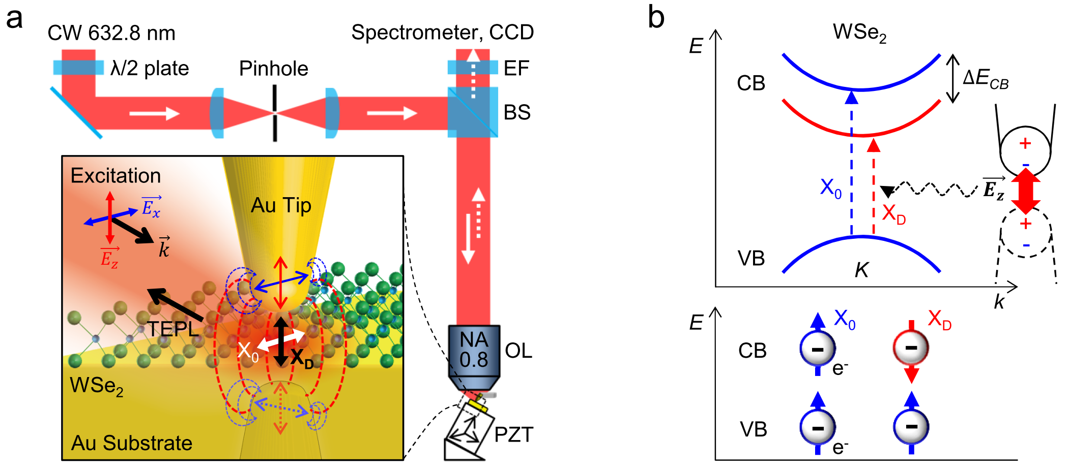 Figure 1
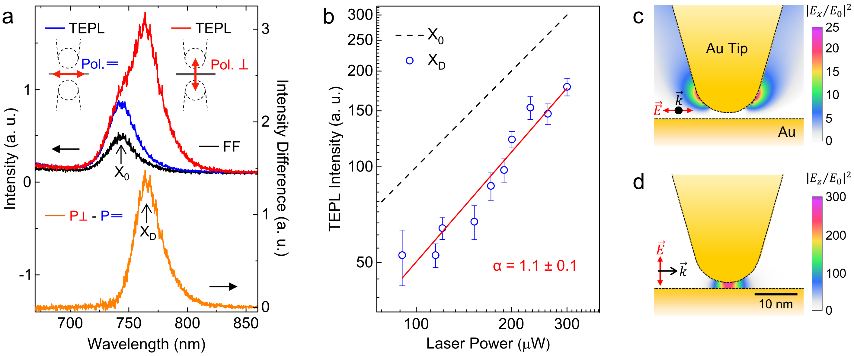 Figure 2
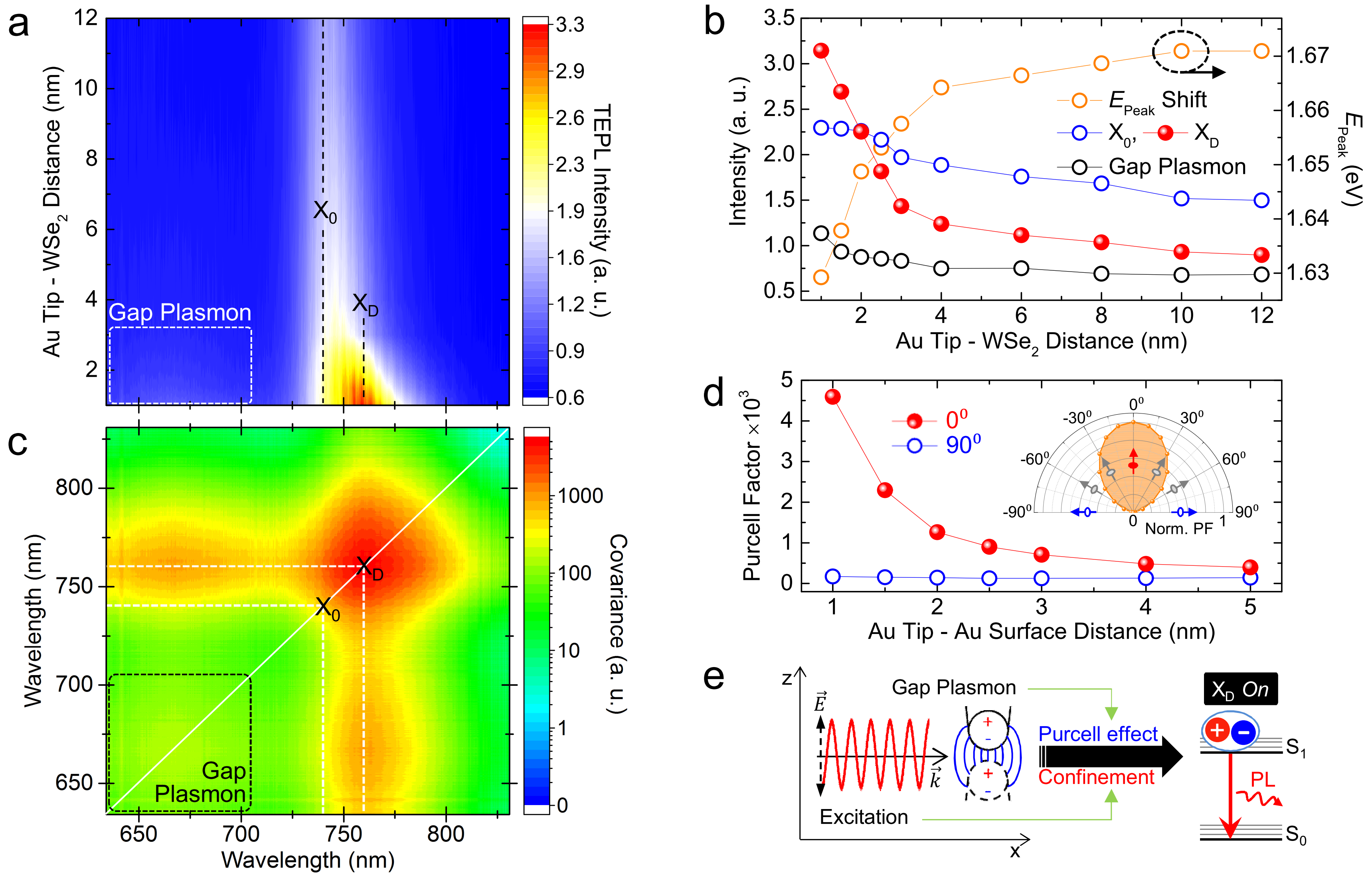 Figure 3
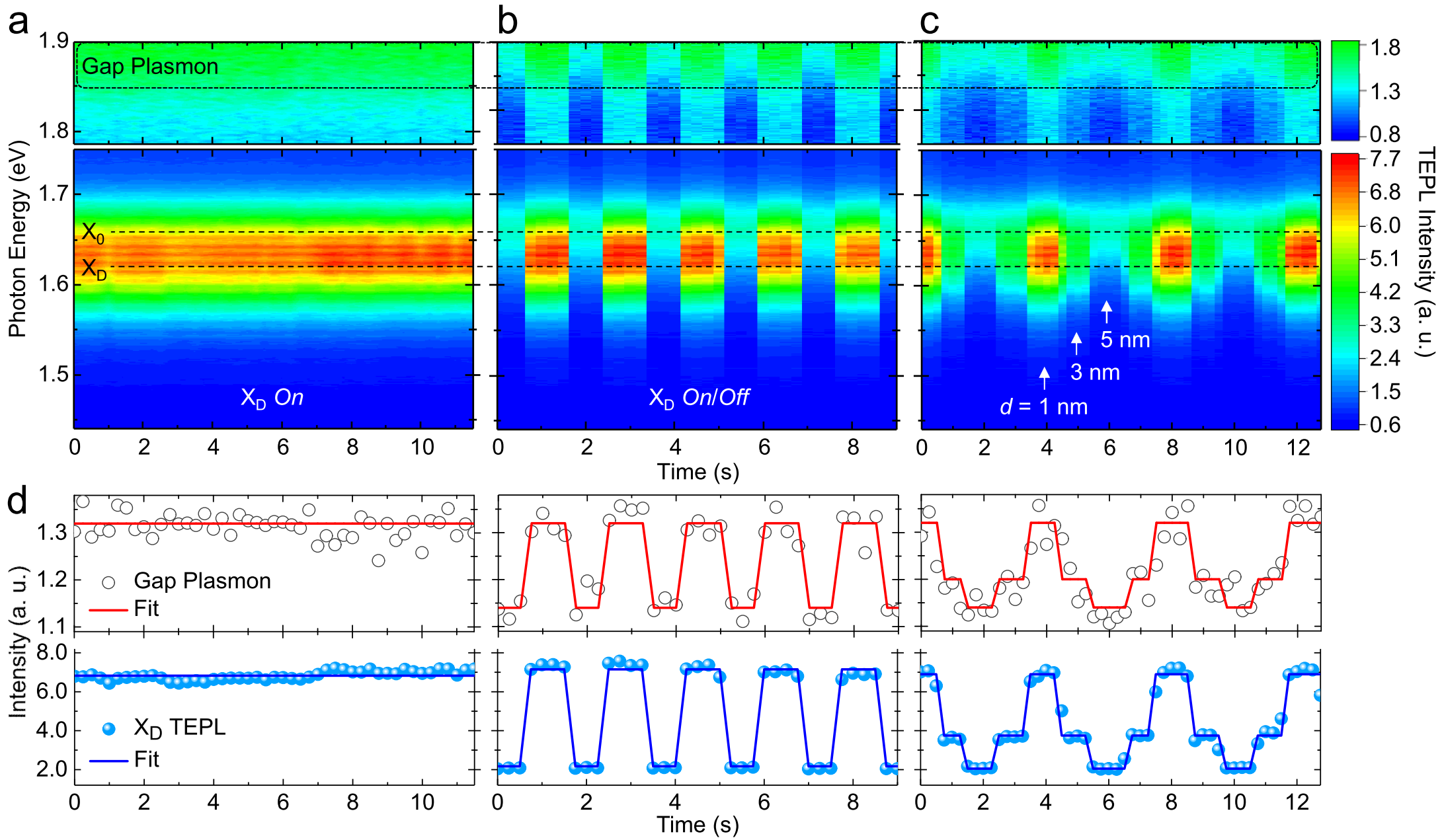 Figure 4
Peer Reviews
No public reviews on file for this paper yet. If you reviewed it on a platform where reviews are public (OpenReview, ICLR, NeurIPS, ICML), you can paste yours below so the community can read it here.
Videos
No videos yet. Explain this paper in a talk, walkthrough, or lecture? Add one.
Radiative control of dark excitons at room temperature by nano-optical antenna-tip induced Purcell effect
Kyoung-Duck Park
Department of Physics, Department of Chemistry, and JILA,
University of Colorado, Boulder, CO, 80309, USA
Tao Jiang
Department of Physics, Department of Chemistry, and JILA,
University of Colorado, Boulder, CO, 80309, USA
Genevieve Clark
Department of Physics, Department of Materials Science and Engineering, University of Washington, Seattle, Washington 98195, USA
Xiaodong Xu
Department of Physics, Department of Materials Science and Engineering, University of Washington, Seattle, Washington 98195, USA
Markus B. Raschke
Department of Physics, Department of Chemistry, and JILA,
University of Colorado, Boulder, CO, 80309, USA
Center for Experiments on Quantum Materials,
University of Colorado, Boulder, CO, 80309, USA
Abstract
Excitons, Coulomb-bound electron and hole pairs, are elementary photo-excitations in semiconductors, that can couple directly to light through radiative relaxation. In contrast to these bright excitons, dark excitons XD with anti-parallel electron spin polarization exist, with generally forbidden radiative emission. Because of their associated long lifetimes, these dark excitons are appealing candidates for quantum computing and opto-electronic devices. However, optical read-out and control of XD states have remained a major challenge due to their decoupling from light. Here, we present a novel tip-enhanced nano-optical approach to precisely switch and programmably modulate the XD emission even at room temperature. Using monolayer two-dimensional transition metal dichalcogenide (TMD) WSe2 on a gold film as model system, we demonstrate -fold enhancement in dark exciton photoluminescence quantum yield. This is achieved by the unique coupling of the nano-optical antenna-tip to the dark exciton out-of-plane optical dipole moment, with an extraordinary Purcell factor of of the tip-sample nano-cavity. Compared to the necessity of cryogenic temperatures and high magnetic fields in conventional approaches, our work provides a new way to harness excitonic properties in low-dimensional semiconductors and new strategies for quantum opto-electronic devices.
The two-dimensional (2D) nature of monolayer (ML) transition metal dichalcogenides (TMDs) creates tightly bound excitons with strong Coulomb interaction and an extraordinarily large binding energy splendiani2010 ; mak2010atomically ; he2014 . Associated anomalous excitonic properties and strong light-matter interaction suggest a new paradigm for a range of applications in optoelectronics mak2016 ; basov2016 ; tong2017 ; hao2016 .
The broken inversion symmetry and strong spin-orbit coupling (SOC) in ML TMDs lead to spin- and energy-splitting in the conduction band kosmider2013 ; echeverry2016 . Associated anti-parallel electron spin configuration gives rise to two distinct states of bright and dark excitons with orthogonal transition dipole orientation, combined with the holes in the higher lying valence band as demonstrated recently both theoretically echeverry2016 ; slobodeniuk2016 and experimentally at low temperature molas2017 ; zhang2016 ; zhou2017 .
As known from zero-dimensional quantum dot (QD) studies, dark excitons XD have a long lifetime due to solely non-radiative decay channels and spin flip processes smolenski2015 . This distinct nature of dark excitons in low-dimensional semiconductors has attracted much attention for potential applications as coherent two-level systems for quantum information processing poem2010 , or Bose-Einstein condensation (BEC) combescot2007 , yet a full-scale study is hampered by the out-of-plane transition dipole moments making them difficult to access optically molas2017 ; zhang2016 ; zhou2017 .
In order to induce dark exciton emission in atomically thin TMDs, different approaches were demonstrated in recent low temperature photoluminescence (PL) studies. Following a procedure as established for dark exciton emission in QDs nirmal1995 ; smolenski2012 , tilting the spin direction by applying a strong external in-plane magnetic field ( 14 T) induces a weakly allowed in-plane optical transition by the Zeeman effect molas2017 ; zhang2016 . Alternatively, by extracting the intrinsically weak out-of-plane optical transition by exciting out-of-plane polarized surface plasmon polaritons (SPP) in a TMD-plasmonic device, weak radiative XD emission through dark exciton-SPP coupling can be induced zhou2017 . However, even then the SPP-induced XD emission is still restricted to cryogenic temperature conditions, due to the small energy difference between dark and bright exciton ensuring low thermal excitation into the otherwise overwhelming bright exciton emission channel.
In this work, we demonstrate a new approach for dark exciton spectroscopy based on state selective dark exciton coupling with tip-enhanced PL (TEPL) spectroscopy, as illustrated in Fig. 1a-b. Here, the scanning probe nano-optical antenna-tip selectively couples to the out-of-plane transition dipole moment which facilitates Purcell-enhanced dark exciton emission with the few-fs radiative dynamics kravtsov2014 . With this simple and generalizable approach we demonstrate excitation, modulation, and radiative control of dark exciton emission, at room temperature, and with high quantum yield. The combination of the nanoscale localized ( 15 nm) effective excitation through strongly confined out-of-plane optical fields at the tip-Au substrate nano-gap, with antenna-tip mediated near- to far-field mode transformation gives rise to a -fold XD-PL enhancement as we demonstrate in WSe2 with a Purcell factor enhanced spontaneous emission rate. From precise atomic force microscopy (AFM) nano-gap distance control of the dark exciton to antenna-tip coupling strength, we achieve from simple switching to active modulation of the dark exciton On/Off states in time and space.
Radiative emission of dark excitons at room temperature
The experiment is based on TEPL spectroscopy park2016tmd , with side illumination of Au nano-tip manipulated in a shear-force AFM as shown schematically in Fig. 1a (see Methods for details). The Au tip is oriented normal with respect to a planar Au substrate. TEPL spectroscopy is then performed by tip-sample distance control between the Au tip and a ML WSe2 transferred onto the Au substrate. All experiments are performed at room temperature.
Fig. 2a shows TEPL spectra at 1 nm tip-sample distance with excitation polarization oriented parallel or perpendicular with respect to the sample surface. A strong XD emission peak is observed (red). In contrast, the XD response is suppressed for tip-perpendicular polarization (blue) even though enhanced PL response of X0 is observed, attributed to an in-plane localized optical field effect in agreement with the spectral X0 characteristics in far-field emission (black). The difference spectrum (orange) then corresponds to the pure XD mode emission. From Lorentzian fitting of the spectra for XD and X0, we obtain meV of intravalley energy splitting between the dark and bright excitons (see Supplementary Fig. S1). This energy difference of XD peak position is in good agreement with recent XD observations facilitated by in-plane magnetic field (47 meV) zhang2016 and SPP coupling (42 meV) zhou2017 . Further the TEPL linewidth of the XD emission is more narrow than the bright exciton linewidth, in agreement with previous observation (see Supplementary Information for details) zhou2017 .
To test for a possible contribution from bi-exciton emission, which has comparable photon energy to dark states, we measure the TEPL intensity as a function of the excitation power for XD and X0 emissions. Fig. 2b shows the resulting TEPL power dependence based on linear fits to the TEPL spectra and plotting the integrated spectral intensities of XD and X0 emissions. On the basis of the linear power dependence behavior, we exclude bi-exciton emission you2015 .
To understand the polarization dependence of the XD emission, and to model the intensity difference of in-plane and out-of-plane local fields at the Au tip - Au substrate junction, we calculate the confined optical field intensity using finite-difference time-domain (FDTD) simulation for our experimental conditions (Fig. 2a). As shown in Fig. 2c-d, in the nano-gap, the optical field intensity of the out-of-plane mode is stronger by a factor of than that of the in-plane mode as expected.
For further investigation of the antenna-tip induced dark exciton emission, we perform TEPL measurements under precise nanometer tip-sample distance control. Fig. 3a shows contour plots of TEPL spectra of ML WSe2 with respect to the distance between the Au tip and Au substrate. Bright exciton emission (X0) at 743.5 nm (1.667 eV) is observed in the distance region of 4 - 12 nm attributed to the enhanced localized (in-plane) near-field excitation at the tip apex. In contrast, for shorter distances in the 1 - 3 nm range, dark exciton XD emission emerges and dominates the spectra at 765 nm (1.621 eV). In addition, a weak tip-plasmon PL response from the Au - Au nano-gap is seen as described previously kravtsov2014 . Fig. 3b shows corresponding distance dependence in TEPL intensity for XD, X0, and gap plasmon emission. While the X0 peak intensity saturates below 2 nm distances due to polarization and energy transfer and non-radiative relaxation in the metal tip and substrate, the XD peak intensity continues to rise sharply correlated with an increasing gap plasmon PL intensity. Because the in-plane dipole of the X0 does not couple to the antenna mode, the PL quenching dominates over enhancement at short distances. In contrast, the XD emission with its out-of-plane dipole, when coupled to the antenna mode with its fs-radiative decay, continues to dominate at short distances kravtsov2014 ; kuhn2006 ; anger2006 .
This behavior is most clearly evident in the 2D covariance plot (Fig. 3c). From the full data set of Fig. 3a, we calculate the covariance between wavelengths and from the distance dependent TEPL intensities using
[TABLE]
The resulting 2D covariance map clearly shows strong (weak) correlation between the out-of-plane gap plasmon and the dark (bright) exciton emission. The plasmon PL emission serves as an indicator and metric of the XD-tip polarization transfer and rapid Purcell enhancement of PL emission as established previously (see Ref. kravtsov2014 and Discussion for details).
Radiative control of dark excitons
As we demonstrated previously park2016tmd , the shear-force AFM tip can also act as an active control element to modify excitonic properties of TMDs both spectrally and spatially. In the optical antenna tip-WSe2-Au surface configuration, the nano-gap is regulated by a shear-force feedback mechanism park2010 . This gives rise to sub-nm precise control of the gap plasmon response, and associated strongly correlated dark exciton emission. Fig. 4a-c show time-series contour plots of the TEPL response (XD, X0, and gap plasmon) during constant (a), discrete (b), and modulated (c) tip-sample distance. The precision of nano-gap control relies on the mechanical quality (Q) factor of the AFM tuning forks. We generally achieve Q-factors of by attaching two Au tips to both prongs of the tuning fork. Using this high-Q sensor, we regulate a tip-sample distance with nm precision, and stably maintain the XD On state under ambient conditions with minimal fluctuations (a). Varying the distance between 1 nm and 5 nm the XD can be switched discretely between its On and Off states (b). Correspondingly, by continuously time-varying the tip-sample distance, we can programmably modulate the XD emission (c). Fig. 4d shows the derived time-series of peak intensity of TEPL response from Fig. 4a-c, with correlation of XD PL and gap plasmon, verifying the precise control of the XD emission.
Radiative decay mechanisms of dark excitons
In 2D TMDs, as dictated by the C3h point group and resulting selection rules, only an out-of-plane optical transition is allowed with times smaller radiative decay rate compared to an in-plane optical transition dipole of the bright excitons echeverry2016 ; slobodeniuk2016 .
In principle, a spin flip is required to induce radiative decay of the dark excitons slobodeniuk2016 . The electron spins can be extrinsically flipped by applying an in-plane magnetic field zhang2016 . Using a large field of 14 T, a radiative decay rate can be obtained with in-plane optical transition by the Zeeman effect molas2017 ; zhang2016 , where is the radiative decay rate of the bright excitons. On the contrary, when the reflection symmetry in the surface normal direction is broken (typical condition for TMD crystals on a flat substrate), an intrinsic spin flip is facilitated by a virtual transition in the conduction band attributed to the SOC mixing. This then induces an out-of-plane dipole transition by the perturbation of a local field bychkov1984 ; slobodeniuk2016 . Since this transition is between quantum states with identical magnetic quantum number and opposite parity, the transition dipole moments give rise to Bychkov-Rashba coupling to an out-of-plane optical field ochoa2013 . The associated radiative decay rate is estimated theoretically echeverry2016 ; slobodeniuk2016 , and is independent of an external field.
In our experimental design, a combination of two physical mechanisms of increase in excitation rate by field enhancement as well as Purcell factor induced optical antenna emission (Fig. 3e) is responsible for the ability to detect the dark exciton modes via tip-coupling to an out-of-plane field. First, a strongly confined out-of-plane optical field effectively excites the transition dipole moment of dark excitons with in the nano-gap enhanced by a factor of compared to the incident field intensity (Fig. 2d). In addition, and most significantly, the spontaneous emission rate is enhanced in the nano-gap due to the plasmonic Purcell effect akselrod2014 ; wang2016 . Here, as demonstrated previously kravtsov2014 , near-field dipole-dipole coupling and exciton polarization transfer into the tip with its few-fs radiative lifetime of its plasmonic optical antenna mode, gives rise to an increased emission of the dark exciton with decreasing tip-sample distance. To model this effect we computationally design out-of-plane and in-plane fluorescent model dipole emitters positioned within the nano-gap to calculate the effective Purcell factor ( = /, See Supplementary Information for details). As shown in Fig. 3d, the Purcell factor of an out-of-plane spontaneous emitter in the tip-surface gap () exceeds for nm distances as a result of the polarization transfer and rapid radiative tip emission.
Enhancement factor of tip-induced dark exciton emission
For our experimental condition, the resulting overall TEPL intensity enhancement factor (EF) of the dark exciton emission as a combination of both effects given by
[TABLE]
is estimated to be as high as at 1.5 nm plasmonic nano-gap. This enhancement factor of the dark excitons is, to the best of our knowledge, the largest enhancement factor for fluorescent emitters investigated to date. In comparison, even refined plasmonic Ag nanocubes coupled to a Ag film achieved -fold fluorescence enhancement from cyanine molecules as the closest analogue rose2014 ; akselrod2014 . This extraordinary PL enhancement is due to the strictly out-of-plane oriented transition dipole moment in the atomically thin semiconductor sandwiched in the 1.5 nm plasmonic nano-gap.
This out-of-plane mode selective enhancement facilitates the room temperature observation of XD not readily possible with other techniques. We can quantify the ratio of near-field TEPL intensity of the dark excitons () compared to the far-field PL intensity of the bright excitons () given by
[TABLE]
Here, and represent respective decay rates, modified by the Purcell factor , and and are relative occupation numbers of thermally populated dark and bright excitons, respectively, with their ratio / given by with the energy splitting between the dark and bright excitons crooker2003 . With the parameters from above, at 300 K, thus facilitating direct probing and active control of the tip-enhanced radiative emission of the dark excitons with strong contrast even at room temperature. However, in the absence of the antenna tip polarization and Purcell effect enhancement, the recently demonstrated dark exciton emission at low temperature by an in-plane magnetic field molas2017 ; zhang2016 and SPP coupling zhou2017 does not readily extend to room temperature due to the dominant spectral weight of the bright excitons.
Conclusions
Our new approach thus gives access to potential applications of dark excitons in quantum nano-optoelectronics over a wide temperature range. We envision the demonstrated tip-antenna platform for room temperature dark exciton emission with or without nano-opto-mechnical control as ideal building block for functional quantum devices. Further, the nanoscale optical switching of the spin states paves way for new design and fabrication of nano-spintronic devices. Specifically, the control of long-lived dark excitons confined in only nm3 mode volume can be exploited to create nanoscale devices for integrated quantum-photonic circuits and active quantum information processor such as nano-light emitting diodes, nano-optical switch/multiplexer, high-density memory, and qubit. The nano-confinement further allows for imaging with 15 nm spatial resolution of heterogeneity of dark excitonic properties in 2D TMDs park2016tmd , with the possibility for an additional modulation in electronic energy with local strain engineering via nano-mechanical tip force control as we demonstrated recently park2016tmd . The range of dynamic controls including coherent ultrafast excitation and tip/antenna manipulation thus gives access to a range of new phenomena at the sub-10 nm scale regime including room temperature strong coupling chikkaraddy2016 ; kleemann2017 , interlayer electron-phonon coupling jin2016 , or out-of-plane exciton behaviors in single molecules and QDs beyond van der Waals materials rivera2016 .
Methods
Sample preparation WSe2 monolayers are grown by physical vapor transport using powdered WSe2 as precursor material. Source material (30 mg) in an alumina crucible is placed in the hot zone of a 25.4 mm horizontal tube furnace, and an SiO2 substrate is placed downstream in a cooler zone at the edge of the furnace ( *∘*C). Before growth, the tube is evacuated to a base pressure of 0.13 mbar and purged several times with argon. The furnace is then heated to 970 *∘*C at a rate of 35 *∘*C/min and remains there for a duration of 5-10 min before cooling to room temperature naturally. A flow of 80 sccm argon and 20 sccm hydrogen is introduced as carrier gas during the 5-10 min growth period. The as-grown WSe2 crystals are then transferred onto flat template stripped Au substrates using a wet transfer technique. For that purpose, PMMA (6% in anisole) is spin-coated onto the SiO2 wafer, covering the region with WSe2 monolayer crystals. The wafer is then placed in a solution of dilute hydrofluoric acid (20% in distilled water), until the SiO2 layer is etched away and the PMMA membrane with WSe2 crystals floats free. The membrane is then rinsed in distilled water to remove residual etchant, and scooped up onto a wire loop. The PMMA membrane can then be placed onto the Au sbstrates under an optical microscope, similar to the commonly used dry transfer technique. Once the membrane has been lowered into contact with the substrate, heating the substrate 160 *∘*C melts the PMMA layer releasing it from the wire loop.
TEPL spectroscopy setup In the TEPL spectroscopy setup, the sample is mounted to a piezoelectric transducer (PZT, P-611.3, Physik Instrumente) with sub-nm precision positioning. Electrochemically etched Au tips ( nm apex radius) are attached to a quartz tuning fork (resonance frequency = kHz) park2016tmd . To regulate the tip-sample distance, the AFM shear-force amplitude is monitored and controlled from the electrically driven tuning fork karrai1995 . Coarse tip positioning is performed using a stepper motor (MX25, Mechonics AG), and shear-force feedback and sample position are controlled by a digital AFM controller (R9, RHK Technology). The sample surface is tilted by ∘ with respect to the incident k-vector for effective excitation. A Helium-Neon laser beam (632.8 nm, 0.3 mW), after passing through a half wave plate for polarization control, is focused into the junction between the Au substrate and the tip apex by an objective lens (NA=0.8, LMPLFLN100, Olympus). TEPL signal is collected in backscattered direction, passed through an edge filter (633 nm cut-off) and detected using a spectrometer (f = 500 mm, SpectraPro 500i, Princeton Instruments) with a thermoelectrically cooled electron-multiplied charge-coupled device (CCD, ProEM+: 1600 eXcelon3, Princeton Instruments). The spectrometer is calibrated using hydrogen and mercury lines, and a 150 grooves/mm grating is used to obtain a high bandwidth spectrum for simultaneous measurement of gap plasmon and TEPL spectra.
The reference list from the paper itself. Each links out to its DOI / PubMed record.
- 1(1) Splendiani, A. et al. Emerging photoluminescence in monolayer Mo S 2 . Nano Letters 10 , 1271–1275 (2010).
- 2(2) Mak, K. F., Lee, C., Hone, J., Shan, J. & Heinz, T. F. Atomically thin Mo S 2 : a new direct-gap semiconductor. Physical Review Letters 105 , 136805 (2010).
- 3(3) He, K. et al. Tightly bound excitons in monolayer W Se 2 . Physical Review Letters 113 , 026803 (2014).
- 4(4) Mak, K. F. & Shan, J. Photonics and optoelectronics of 2D semiconductor transition metal dichalcogenides. Nature Photonics 10 , 216–226 (2016).
- 5(5) Basov, D., Fogler, M. & de Abajo, F. G. Polaritons in van der Waals materials. Science 354 , aag 1992 (2016).
- 6(6) Tong, Q. et al. Topological mosaics in moire superlattices of van der Waals heterobilayers. Nature Physics 13 , 356–362 (2017).
- 7(7) Hao, K. et al. Direct measurement of exciton valley coherence in monolayer W Se 2 . Nature Physics Online Publication (2016).
- 8(8) Kośmider, K., González, J. W. & Fernández-Rossier, J. Large spin splitting in the conduction band of transition metal dichalcogenide monolayers. Physical Review B 88 , 245436 (2013).