Power- and Spectral Efficient Communication System Design Using 1-Bit Quantization
Hela Jedda, Muhammad Mudussir Ayub, Jawad Munir, Amine Mezghani and, Josef A. Nossek
TL;DR
This paper proposes a joint optimization approach for power amplifier and pulse shaping filter parameters in a 1-bit quantized SISO communication system to maximize combined power and spectral efficiency.
Contribution
It introduces a novel joint optimization framework for power and spectral efficiency in 1-bit quantized systems, balancing tradeoffs between power consumption and spectral use.
Findings
Optimal system parameters identified through simulations
Enhanced power and spectral efficiency achieved
Guidelines for pulse shaping and amplifier design provided
Abstract
Improving the power efficiency and spectral efficiency of communication systems has been one of the major research goals over the recent years. However, there is a tradeoff in achieving both goals at the same time. In this work, we consider the joint optimization of the power amplifier and a pulse shaping filter over a single-input single-output (SISO) additive white Gaussian noise (AWGN) channel using 1-bit analog-todigital (ADC) and digital-to-analog (DAC) converters. The goal of the optimization is the selection of the optimal system parameters in order to maximize the desired figure-of-merit (FOM) which is the product of power efficiency and spectral efficiency. Simulation results give an insight in choosing the optimal parameters of the pulse shaping filter and power amplifier to maximize the desired FOM.
Peer Reviews
No public reviews on file for this paper yet. If you reviewed it on a platform where reviews are public (OpenReview, ICLR, NeurIPS, ICML), you can paste yours below so the community can read it here.
Videos
No videos yet. Explain this paper in a talk, walkthrough, or lecture? Add one.
Power- and Spectral Efficient Communication System Design Using 1-Bit Quantization
Hela Jedda, Muhammad Mudussir Ayub, Jawad Munir, Amine Mezghani and Josef A. Nossek
Institute for Circuit Theory and Signal Processing
Munich University of Technology, 80290 Munich, Germany
E-Mail: {hela.jedda, josef.a.nossek}@tum.de
Abstract
Improving the power efficiency and spectral efficiency of communication systems has been one of the major research goals over the recent years. However, there is a trade-off in achieving both goals at the same time. In this work, we consider the joint optimization of the power amplifier and a pulse shaping filter over a single-input single-output (SISO) additive white Gaussian noise (AWGN) channel using -bit analog-to-digital (ADC) and digital-to-analog (DAC) converters. The goal of the optimization is the selection of the optimal system parameters in order to maximize the desired figure-of-merit (FOM) which is the product of power efficiency and spectral efficiency. Simulation results give an insight in choosing the optimal parameters of the pulse shaping filter and power amplifier to maximize the desired FOM.
Index Terms:
Green Communication, Power Efficiency, Spectral Efficiency, 1-Bit Quantization.
††publicationid: pubid: 978-1-4673-6540-6/15/$31.00 © 2015 IEEE
I Introduction
The demand for higher throughput and capacity is increasing at a staggering rate per year for cellular networks. Higher cell density, greater amount of usable spectrum and higher spectral efficiency are considered as key possibilites to realize such an increase in capacity [1]. The deployment of very large number of antennas, also known as massive MIMO, at the base station is considered as key enabler to meet very high data requirements.
One of the major limiting factors for the implementation of massive MIMO are the complexity issues and the power consumption of the RF components due to the large number of antennas. Several approaches are considered in the literature to decrease the power consumption such as spatial modulation [2], the use of parasitic antennas [3] and the use of low-cost transceivers [4]. One attractive solution is the use of very low resolution ADCs and DACs, because the power consumption increases exponentially with resolution [5]. The extreme case of -bit ADCs and DACs is particularly very interesting because it can greatly simplify and decrease the power requirements of the other RF front-end components such as power amplifiers (PA), low-noise amplifiers (LNA) etc.
The price to pay for the -bit is the severe signal distortion due to the strong non-linear operation. It also causes both in-band and out-of-band radiation (OBR) resulting in the degradation of the bandwidth efficiency. Therefore, the potential advantages of -bit systems have to be supported by new signal processing algorithms and RF front-end architectures to achieve bandwidth efficiency and spectral efficiency. In this paper, we investigate the effect of pulse shaping and optimum operating region of the power amplifier for a -bit DAC and ADC at the transmitter and receiver side, respectively. As a basic investigation of possible receiver and transmitter structures, we consider the SISO case and we leave the MIMO case for future investigation.
The paper is organized as follows: First, the SISO system model is introduced in Section II. Section III describes the general power model of different components in a wireless transceiver front-end. Performance metrics and the optimization problem are given in Section IV and Section V, respectively. Section VI analyzes the optimal system parameters that solve the optimization problem.
II System Model
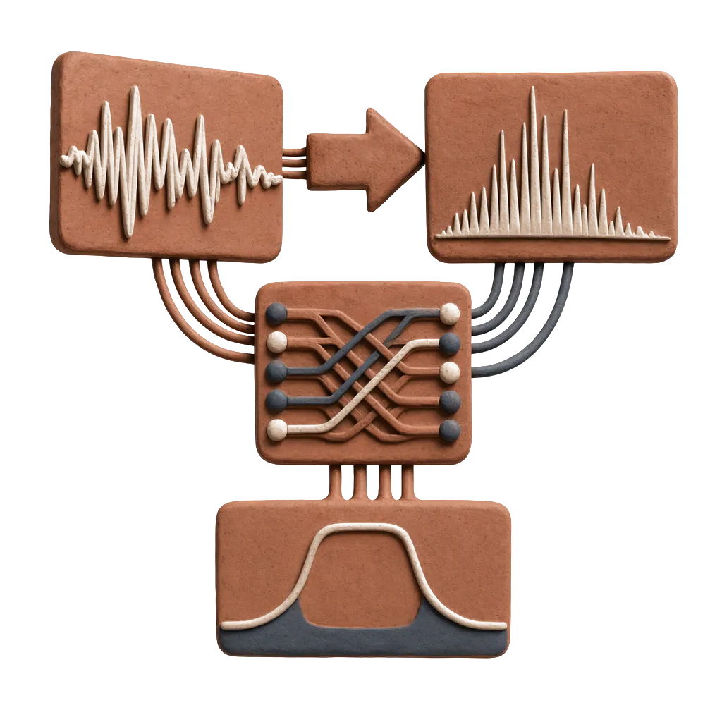
Consider the block diagram of a communication system transmitting QPSK symbols generated at a baud rate of depicted in Fig. 1. In the transmitter, the QPSK symbols are shaped by a discrete-time root-raised cosine (RRC) filter. The resulting baseband signal is converted to the analog domain, utilizing two DACs for the inphase and quadrature components. The low-pass filter (LPF) removes the DACs’ alias spectra. The baseband signal is then translated to the RF carrier frequency by the upconversion mixer. The PA generates the required output power of the signal and delivers it to the antenna. The transmitted signal of power propagates through an AWGN channel between the transmitter and receiver in the form of an electromagnetic wave and gets disturbed by some Gaussian distributed noise of power spectral density . The signal-to-noise ratio (SNR) is then defined as , where represents the constant channel power gain and . The signal captured by the receiver antenna is amplified by an LNA and converted into a baseband signal and then filtered by a LPF to limit the noise bandwidth. In this work, an ideal LNA will be considered since its power consumption is in general quite negligible [6]. The baseband signal is converted into discrete-time using two ADCs for the inphase and quadrature components. After the ADCs, the RRC filter of the receiver completes the pulse shape to fulfill the Nyquist inter-symbol-interference (ISI) criterion and the sampling rate is reduced to the baud rate . In this work, three system models are considered. Sys1 designates the above described system with infinite resolution DAC/ADC. Sys2 is the same system model but with restriction of 1-bit DAC/ADC. Sys3 differs from sys2 through the removal of RRC and the upsampling at the transmitter side. In this case, the pulse shaping is realized by the LPF and the band pass filter (BPF) of the PA.
The total power consumed by the communication system can be divided into two major parts: power consumed by the analog front-end components and power of digital signal processing :
[TABLE]
The aim of this contribution consists in reducing . The power consumed by the analog front-end components can be given as:
[TABLE]
where , and are the powers consumed by the PA, DAC and ADC, respectively.
To this end, these three components will be investigated in more detail.
III Power Model
III-A Power Amplifier (PA)
The PA is a non-linear device which clips the output signal if the input signal is greater than a certain value. Non-linearities of the PA cause interferences and distortions, which create in-band and out-of-band spectral spread [7]. To quantify , a model of PA has to be first introduced and then a closed form for calculation can be given.
III-A1 Modeling and Implementation
The PA is a critical component in wireless communication systems and correct modeling of its non-linearities are of utmost importance. The dominant PA distortion source is the amplitude distortion or AM-AM conversion. It describes the relation between the amplitudes of the PA’s input and output signals [8]. The AM-AM distortion can incorporate most of the PA non-linear effects [9]. The PA is modeled as a transformer based push-pull stage as depicted in Fig. 2, where is the supply voltage, is the bias voltage for the transistor, is the load current and is the load resistance of the antenna. This model is called push-pull because only one transistor is on at a time. It behaves as a voltage controlled current source if the input voltage is small and for higher input values it starts behaving as a switch. For a given PA input signal , under single carrier and narrow band assumption, the output signal , which is affected by the AM-AM distortion, can be given by:
[TABLE]
where , and represent the amplitude, the carrier frequency and the phase of the PA input signal . If the input signal exceeds , the output signal is set to . The signal goes then through the BPF built by two capacitances and two inductances. This BPF has the impulse response and the bandwidth , which can be adjusted by the choice of the reactances. The PA output signal is the band-pass filtered version of , , and can be given in the following way:
[TABLE]
The resulting AM-AM transfer characteristic is a soft limiter type non-linearity and plotted in Fig. 3.
III-A2 Power consumption
The power consumed from the battery by the push-pull model can be calculated as [6]:
[TABLE]
The output current is directly controlling . The output current is a function of the input signal as it is behaving as a voltage controlled current source before running into saturation region at high input values. Before concluding the PA section, one important parameter in which we are interested is the input back-off (IBO) of the push-pull model. The IBO in push-pull model can be considered as the amount of clipping introduced in the signal [6]. It can be given as:
[TABLE]
where is the variance of the input signal . is measured in terms of voltage. The PA runs in the non-linear region if the IBO value is small as the saturation value gets smaller than .
The average output power of the push-pull model , that is the power consumed by the antenna load , is expressed as:
[TABLE]
III-B Power consumption of DAC/ADC
The power consumptions of the ADC and DAC scale exponentially with the resolution as shown in [10] and [11]. The extreme case of -bit ADC and DAC architecture consumes the least amount of power. Motivated by this fact, the optimal system parameters using -bit ADC and DAC are investigated for reduced overall power consumption.
IV Performance measures
Before formulating the problem, some performance measures have to be first introduced.
IV-A Information rate
The information rate is given in bits per second and is defined as:
[TABLE]
where is the mutual information between the sent and received signals and defined as:
[TABLE]
where denotes the probability mass function (pmf). Memory effects of the filters are neglected. In the simulations, the mutual information is estimated based on the numerical method introduced in [12], in order to take the different effects of communication chain into account, especially the nonlinear effects of the PA and the DAC/ADC.
IV-B Signal bandwidth
The signal bandwidth designates the bandwidth of the transmitted signal at the output of the PA . Since the 3dB bandwidth definition does not inform us about the amount of OBR, another definition of the bandwidth is required. To this end, the signal-to-interference-noise ratio (SINR) is taken into account, wich is defined as SINR, where denotes the interference power of both adjacent channels spaced by with the assumption that . For an SINR value of 10dB we get the 93,75% bandwidth :
[TABLE]
where is the power sprectral density of the PA output signal . The remaining § of the signal power lying outside the defined bandwidth (OBR) is then considered as .
IV-C Transmit power efficiency
The transmit power efficiency measures the required PA power consumption for achieving the maximal information rate:
[TABLE]
The higher , the better the PA power is utilized.
IV-D Transmit spectral efficiency
The transmit spectral efficiency measures the rate, at which information in bits per second can be transmitted in each Hz of bandwidth :
[TABLE]
The larger , the better the bandwidth is utilized.
V Problem Formulation
In this contribution, the aim is to minimize the total power consumption of the wireless communication system through reducing the power consumed by the analog components . To this end, the power consumptions of the DAC, ADC and PA have to be reduced. The minimal power consumption of DAC and ADC can be reached by using 1-bit resolution. Thus, it remains to reduce the PA power consumption . Therefore, the goal of this work consists in finding the optimal PA parameters: IBO and , that maximize the transmit spectral effciency as well as the transmit power efficiency of a SISO wireless communication system with QPSK modulation and using 1-bit ADC/DAC. On one hand, increasing means reducing which implies reducing IBO. However, low IBO, i.e. low clipping ratio, results in a large amount of OBR. The latter increases the signal bandwidth and thus decreases . On the other hand, low can reduce the OBR which decreases and thus increases . Therefore, maximizing as well as maximizing are conflicting goals [13]. An optimal compromise is achieved by maximizing the product of both:
[TABLE]
The FOM is defined as: . Since the problem only involves two variables, it can be solved based on numerical simulations using the Grid-Search method.
VI Simulation Results
For the simulations, we choose a carrier frequency of . The RRC filters have roll-off factor of . The LPF is a 4th order Butterworth filter of 3-dB bandwidth equal to . The PA includes a 4th order band-pass filter of 3-dB bandwidth around . The simulations are run with of QPSK symbols. The SINR is set to dB. First simulations are done with sys2 and then all three systems are compared.
The aim is to find IBO and , that maximize the FOM, i.e. that jointly maximize the information rate and minimize the PA power consumption and the signal bandwidth . Therefore, , and are studied for different values of IBO and .
In Fig. 4, the inverse of the PA efficiency is plotted as function of IBO. This increases exponentially with IBO. For low IBO, the clipping ratio is very small. The PA operates in the non-linear region. Therefore, the PA power consumption decreases. So, it is interesting to run the PA at low IBO to reduce . However, the effect of low IBO at and for different values has to be investigated. In the simulation set depicted in Fig. 5 and Fig. 6, the information rate and the signal bandwidth normalized by , and are plotted as functions of IBO for different PA BPF bandwidths . The lower IBO, the more the PA works in the non-linear region. That means the PA input signal gets more clipped which increases the OBR at the PA output. The amount of OBR can be restricted by the choice of . As can be seen in the simulation results, for low IBO the decreases slightly while increases. However, the decrease in and the increase in depends on the used BPF. The larger , the less the removed OBR and thus the larger . The decrease in leads to a decrease in . However, the further decrease in leads to a decrease in . Therefore, has to be optimized to increase the FOM.
In Fig.7, the FOM is plotted as function of IBO for different . The FOM is maximized and saturated for low IBO and starts decreasing from IBO=1. The maximal value of FOM depends on . It can be concluded that there is an optimal that maximizes the FOM at low IBO. The optimal value of can be extracted from Fig. 8. Thus, IBO and are the optimal operating points that solve the optimization problem for sys2.
In the last simulation set, all three systems sys1, sys2 and sys3 introduced in section II are considered. In Fig. 9, the FOM is plotted as function of for the three introduced system models at IBO. Sys1 is used as the benchmark. As can be seen from the figure, the FOM is maximized at for sys1, sys2 and sys3, respectively. The simulation results show that there is a loss in FOM of sys2 compared to sys1. This loss is due to the reduction of the DAC/ADC resolution to 1-bit. However, almost half of this loss can be recovered in sys3 by removing the RRC filter before the 1-bit DAC at the transmitter. In sys2, the QPSK symbols are pulse shaped by an RRC filter and then quantized by the 1-bit DAC. The output of the 1-bit DAC is again QPSK. So what is the need for the pulse shaper? The idea with sys3 is to keep the QPSK symbols without digital signal processing so that the output of the 1-bit DAC consists of the same QPSK symbols but in the analog domain. There is no quantization loss in this case. Note that the total power consumption of sys3 is largely decreased compared to of sys1, since 1-bit DAC/ADC are used and the RRC filter at the transmitter is removed.
VII Conclusion
In this work, it is shown that the PA can be run in the non-linear region with an appropriate BPF while maximizing the power and spectral efficency in the SISO system with the QPSK modulation scheme and using 1-bit quantization. Additionally, the removal of the RRC filter at the transmitter side is beneficial in terms of the introduced FOM. The FOM gets improved and the circuit complexity at the transmitter is decreased. For future work, one can look for the optimal analog pulse shaper at the transmitter side in the presence of 1-bit DAC. Furthermore, the same performance analysis can be investigated while considering the AM-PM distortion of the PA. Moreover, the loss due to the 1-bit quantization can be recovered by oversampling in time and in space. Then, the analysis can be generalized to the MIMO case.
The reference list from the paper itself. Each links out to its DOI / PubMed record.
- 1[1] S. Rangan, T. Rappaport, and E. Erkip, “Millimeter-wave cellular wireless networks: Potentials and challenges,” Proceedings of the IEEE , vol. 102, no. 3, pp. 366–385, March 2014.
- 2[2] M. Di Renzo, H. Haas, A. Ghrayeb, S. Sugiura, and L. Hanzo, “Spatial modulation for generalized mimo: Challenges, opportunities, and implementation,” Proceedings of the IEEE , vol. 102, no. 1, pp. 56–103, Jan 2014.
- 3[3] A. Kalis, A. Kanatas, and C. Papadias, Parasitic Antenna Arrays for Wireless MIMO Systems . Springer, 2014.
- 4[4] E. Bjornson, M. Matthaiou, and M. Debbah, “Massive MIMO with Non-Ideal Arbitrary Arrays: Hardware scaling laws and circuit-aware design,” Wireless Communications, IEEE Transactions on , vol. PP, no. 99, pp. 1–1, 2015.
- 5[5] C. Svensson, S. Andersson, and P. Bogner, “On the power consumption of analog to digital converters,” in Norchip Conference, 2006. 24th , Nov 2006, pp. 49–52.
- 6[6] A. Mezghani and J. Nossek, “Modeling and minimization of transceiver power consumption in wireless networks,” in Smart Antennas (WSA), 2011 International ITG Workshop on , Feb 2011, pp. 1–8.
- 7[7] D. R. Morgan, Z. Ma, J. Kim, M. G. Zierdt, and J. Pastalan, “A generalized memory polynomial model for digital predistortion of rf power amplifiers,” Signal Processing, IEEE Transactions on , vol. 54, no. 10, pp. 3852–3860, 2006.
- 8[8] S. Ali and E. Arabi, “Behavioral modeling of rf front end devices in simulink,” Master’s thesis, Signal processing group, Department of Signals and Systems, Chalmers University of Technology, 2008.