Optical charge state control of spin defects in 4H-SiC
Gary Wolfowicz, Christopher P. Anderson, Andrew L. Yeats, Samuel J., Whiteley, Jens Niklas, Oleg G. Poluektov, F. Joseph Heremans, and David D., Awschalom

TL;DR
This paper demonstrates bidirectional optical control of charge states in silicon carbide defects, significantly enhancing photoluminescence and enabling stable, long-term charge state manipulation for quantum technology applications.
Contribution
It introduces a method for optical charge state control of divacancy and silicon vacancy defects in 4H-SiC, with stable, hours-long charge state persistence and a comprehensive defect model.
Findings
Up to three orders of magnitude increase in photoluminescence with near-UV excitation
Stable charge state control for hours at cryogenic temperatures
Bidirectional optical charge conversion between bright and dark states
Abstract
Defects in silicon carbide (SiC) have emerged as a favorable platform for optically-active spin-based quantum technologies. Spin qubits exist in specific charge states of these defects, where the ability to control these states can provide enhanced spin-dependent readout and long-term charge stability of the qubits. We investigate this charge state control for two major spin qubits in 4H-SiC, the divacancy (VV) and silicon vacancy (Vsi), obtaining bidirectional optical charge conversion between the bright and dark states of these defects. We measure increased photoluminescence from VV ensembles by up to three orders of magnitude using near-ultraviolet excitation, depending on the substrate, and without degrading the electron spin coherence time. This charge conversion remains stable for hours at cryogenic temperatures, allowing spatial and persistent patterning of the relative charge…
Click any figure to enlarge with its caption.
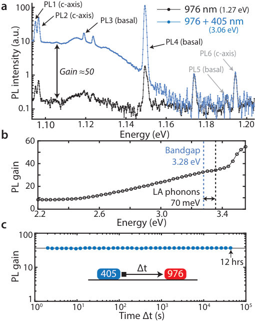 Figure 1
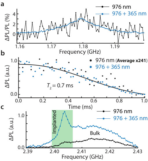 Figure 2
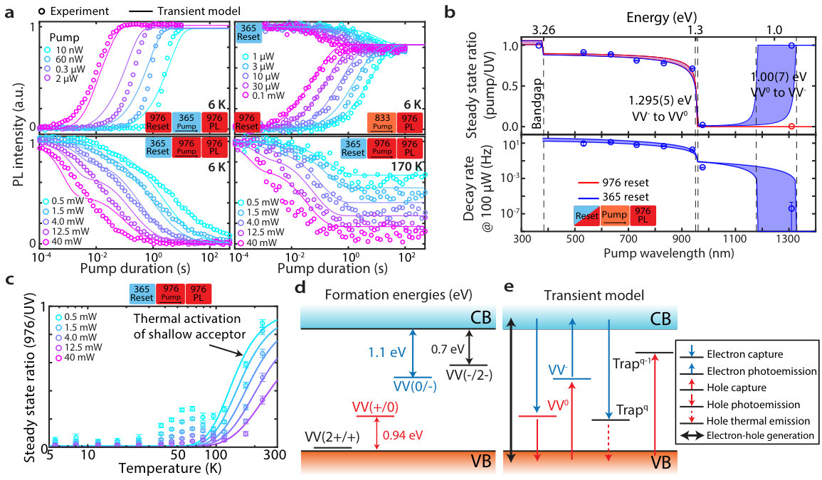 Figure 3
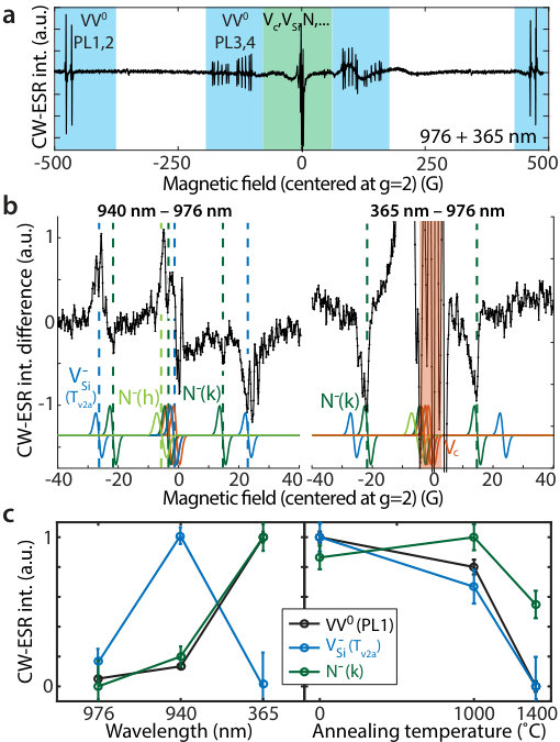 Figure 4
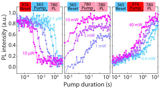 Figure 5
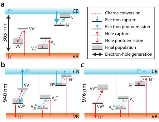 Figure 6
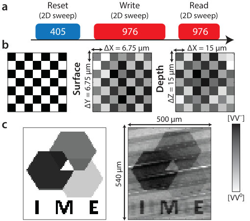 Figure 7
Peer Reviews
No public reviews on file for this paper yet. If you reviewed it on a platform where reviews are public (OpenReview, ICLR, NeurIPS, ICML), you can paste yours below so the community can read it here.
Videos
No videos yet. Explain this paper in a talk, walkthrough, or lecture? Add one.
Optical charge state control of spin defects in 4H-SiC
Gary Wolfowicz
Institute for Molecular Engineering, University of Chicago, Chicago, Illinois 60637, USA
WPI-Advanced Institute for Materials Research (WPI-AIMR), Tohoku University, Japan
Christopher P. Anderson
Institute for Molecular Engineering, University of Chicago, Chicago, Illinois 60637, USA
Department of Physics, University of Chicago, Chicago, Illinois 60637, USA
Andrew L. Yeats
Institute for Molecular Engineering, University of Chicago, Chicago, Illinois 60637, USA
Materials Science Division, Argonne National Laboratory, Lemont, Illinois 60439, USA
Samuel J. Whiteley
Institute for Molecular Engineering, University of Chicago, Chicago, Illinois 60637, USA
Department of Physics, University of Chicago, Chicago, Illinois 60637, USA
Jens Niklas
Chemical Sciences and Engineering Division, Argonne National Laboratory, Lemont, Illinois 60439, USA
Oleg G. Poluektov
Chemical Sciences and Engineering Division, Argonne National Laboratory, Lemont, Illinois 60439, USA
F. Joseph Heremans
Materials Science Division, Argonne National Laboratory, Lemont, Illinois 60439, USA
Institute for Molecular Engineering, University of Chicago, Chicago, Illinois 60637, USA
David D. Awschalom
Institute for Molecular Engineering, University of Chicago, Chicago, Illinois 60637, USA
Materials Science Division, Argonne National Laboratory, Lemont, Illinois 60439, USA
Abstract
Defects in silicon carbide (SiC) have emerged as a favorable platform for optically-active spin-based quantum technologies. Spin qubits exist in specific charge states of these defects, where the ability to control these states can provide enhanced spin-dependent readout and long-term charge stability of the qubits. We investigate this charge state control for two major spin qubits in 4H-SiC, the divacancy (VV) and silicon vacancy (VSi), obtaining bidirectional optical charge conversion between the bright and dark states of these defects. We measure increased photoluminescence from VV ensembles by up to three orders of magnitude using near-ultraviolet excitation, depending on the substrate, and without degrading the electron spin coherence time. This charge conversion remains stable for hours at cryogenic temperatures, allowing spatial and persistent patterning of the relative charge state populations. We develop a comprehensive model of the defects and optical processes involved, offering a strong basis to improve material design and to develop quantum applications in SiC.
Optically active color centers in wide bandgap semiconductors have shown considerable potential for a variety of spin-based quantum technologies, from quantum computing and quantum memories Waldherr et al. (2014) to nano-scale sensing Maze et al. (2008); Toyli et al. (2013); Kucsko et al. (2013). Spin defects in silicon carbide (SiC) in particular combine the optical properties required for single-spin measurements (Baranov et al. (2011); Koehl et al. (2011); Kraus et al. (2013); Christle et al. (2014); Widmann et al. (2014); Christle et al. (2017)) with wafer-scale growth and silicon-like fabrication capabilities developed for high-power electronics. However, optimizing these systems for spin qubit applications requires an understanding of not only their spin and optical properties, as demonstrated in the negatively charged silicon vacancy (V) Janzén et al. (2009); Baranov et al. (2011) and the neutral divacancy (VV0) Torpo et al. (2002); Son et al. (2006); Falk et al. (2013a); Christle et al. (2017), but also an understanding of their charge properties.
Impurities in SiC and their charge states have been investigated for conventional electronics applications, as they play an important role in transport properties and in carrier compensation. Most studies involve deep level transient spectroscopy (DLTS) Booker et al. (2014, 2016), electron spin resonance (ESR) Matsumoto et al. (1997); Isoya et al. (2008) and density functional theory (DFT) Gali (2012); Gordon et al. (2015); Weber et al. (2011) with a strong focus on the carbon vacancy (VC) Umeda et al. (2005); Son et al. (2012); Booker et al. (2016); fewer works have addressed VSi and VV defects Umeda et al. (2009). For the purpose of quantum information, it is desirable to understand the complete physics of the defects themselves, not just their influence on transport or other electrical characteristics of the substrate.
Here, we investigate the effect of optical illumination on the stability of the relevant (optically bright) charge states of VV and VSi, the ability to control and convert these states between different charge levels, and the implications for quantum applications. We investigate these questions using a combination of techniques including photoluminescence (PL), optically-detected magnetic resonance (ODMR) and electron spin resonance (ESR). The VV and VSi charge states are both stabilized to the VV0 and V states required to observe PL, whose intensity can be enhanced by up to three orders of magnitude depending on the material (local defect concentrations and Fermi level). For VV in particular, we observe bidirectional charge conversion between the neutral (bright qubit state) and negative charge states using mainly near-ultraviolet (365-405 nm) and near-infrared (976 nm) light. This charge conversion is stable at cryogenic temperature and does not affect the ODMR contrast nor the electron spin coherence time, and can therefore be readily applied to increase PL emission from ensembles.
Charge state conversion can have multiple origins, including direct photoionization, free carrier recombination, and charge transfer between defects. In order to fully understand the involved processes, we measure the charge dynamics of VV, VSi and nitrogen (N) under illumination, where N is the main dopant in our semi-insulating 4H-SiC samples. Excitation dependence with wavelengths ranging from 365 nm to 1310 nm were measured and simulated, offering a comprehensive picture of charge transfer between these defects. In particular, this allows us to identify that VV0 converts to the dark VV- charge state under 976 nm illumination, while V will convert to the dark V charge state with above-bandgap light.
Control and understanding of these charge dynamics is crucial for maximizing spin qubit readout, choosing adequate background impurity concentrations in samples and optimizing designs of SiC nano-devices for quantum applications. Such methods have also been applied in the nitrogen-vacancy (NV) center in diamond for quantum optics applications Aslam et al. (2013), enabling for example reduced spectral diffusion Siyushev et al. (2013) or Stark tuning of the optical transitions through photoexcitation of trapped charges Bassett et al. (2011). More exotic applications of charge dynamics include high density data storage Dhomkar et al. (2016), STED super-resolution imaging Han et al. (2010); Chen et al. (2015) and charge quantum buses Doherty et al. (2016).
I Results
I.1 PL enhancement using UV illumination
We initially observe a drastic increase in PL intensity of VV0, by about 50 times, when continuously illuminating a semi-insulating 4H-SiC sample with a 405 nm (”UV”) laser diode, in addition to the 976 nm laser required for PL excitation. This is shown in Figure 1(a) where the full PL spectrum for all the divacancies (PL1 to PL6 Koehl et al. (2011)) is taken with (blue) and without (black) 405 nm excitation. Both c-axis (PL1, PL2) and basal defects (PL3, PL4) show an increase in their PL intensity, with slight variation between defects, which we ascribe to charge conversion of the divacancy toward its observable neutral state. On the other hand, PL5 and PL6 remain completely unaffected, adding another unique feature to these currently unidentified defects on top of their strong room temperature PL emission. The VV0 PL enhancement with UV was observed in all semi-insulating wafers we measured, with gains ranging by a factor of 2 to 1000 (see Supplementary Figure 2), including samples obtained from separate commercial suppliers (Cree or Norstel), different growth batches, or even simply from separate positions within the same wafer. This strongly indicates an influence from the local environment, e.g. from the remaining concentration of N dopants or other impurities which is known to locally differ in as-grown wafers Jenny et al. (2004). The PL intensity with UV remains fairly constant however from sample to sample.
In order to understand the effect of 405 nm illumination, and optimize the enhancement, the excitation wavelength is swept across the 4H-SiC bandgap energy (3.28 eV, 380 nm) as shown in Figure 1(b). The PL gain slowly increases with excitation energy, and around 3.33-3.35 eV, slightly above the 4H-SiC bandgap (3.28 eV), it drastically turns up. This suggests two separate processes are altering the VV charge state from either VV- or VV+ to VV0: at low energies, we will see this is due to direct photoionization, while at high energies, the gain results from recombination of generated electron-hole pairs.
We now consider charge dynamics under illumination, starting from the stability of the conversion observed after UV excitation. As illustrated in Figure 1(c), the system is initially pumped with 405 nm toward a high VV0 population (strong PL intensity), followed by a long delay to allow for relaxation and finally measurement using 976 nm. No change is observed over the course of 12 hours, a result largely expected for a deep defect at cryogenic temperature (6 K). More interestingly, the PL intensity always drops to a low level after turning off the UV excitation while 976 nm was continuously on. Combined with this long stability, this implies that the use of 976 nm to excite VV PL is simultaneously converting the VV out of its neutral charge state, toward a dark state (more details are given later on). This has significant consequences as wavelengths near 976 nm have been extensively used in recent PL- and ODMR-related works Christle et al. (2014); Zargaleh et al. (2016); Seo et al. (2016), owing to being close to the absorption maximum of the ground to excited state transition of VV0, as well as being easily available commercially. These previous studies may therefore have been partially perturbed by charge conversion.
I.2 Illumination effects on spin properties
Above-bandgap excitation can be used to efficiently convert VV toward its neutral charge state, and more importantly drastically increases the PL intensity. For practical applications however, we verify this has no effect on the spin properties of VV0. In Figure 2(a), we first measure the ODMR contrast of PL2, i.e. the ratio of ODMR over PL intensity, which provides a direct measure of how the spin states may be affected during illumination. For these experiments, the 405 nm laser is replaced by a 365 nm (also called ”UV”) light-emitting diode which is more efficient at charge conversion since it is above bandgap in energy. No difference in contrast is observed with or without 365 nm, and the charge conversion therefore does not significantly affect the spin state nor the readout mechanism. However, the signal-to-noise ratio improves by 70 times with illumination due to increased VV0 charge population. More details are given in the Supplementary Figure 6 and Supplementary Note 2 regarding the ODMR experiments presented here.
A second crucial property is the electron spin coherence of the defect. From Figure 1(c), the charge stability at cryogenic temperature (6 K) is shown to be much longer than any coherence timescale Seo et al. (2016), however we check that even with constant 365 nm illumination (0.2 mW) and corresponding electron-hole pair generation, the coherence time remains unaffected. At 400 G, the ensemble electron spin coherence is measured to be 0.7 ms and remains completely unaffected by either light or free carriers (Figure 2(b)), while much longer averaging () was required to obtain similar signal-to-noise ratios without 365 nm illumination. This is not an obvious result as scattering or exchange interaction with free carriers can easily reduce or of defect spins Tyryshkin et al. (2011).
Until now, all measurements were realized on as-grown commercial wafers with naturally occurring impurity concentrations. However, carbon ion implantation or electron irradiation Falk et al. (2013b) is often used to increase the PL intensity and to improve spatial resolution. The type of defects created by lattice damage during these processes cannot be well controlled however, though partially manageable using annealing, and the local Fermi level may shift away from obtaining a desired charge state. We test this with a 500 nm thick layer of implanted divacancies (see Methods section). When measuring the PL2 ODMR spectrum of this sample, as shown in Figure 2(c), we obtain a broad “bulk” signal observable across the entire sample depth using simply 976 nm excitation. When 365 nm is turned on (with constant absorption over the sample depth), the bulk intensity increases as expected, but more importantly a narrower and more intense peak appears. The latter is assigned to the implanted layer which, being confined in depth, is less sensitive to inhomogeneity in the static magnetic field. Rabi experiments at the peak layer frequency yielded as expected an increased contrast (Supplementary Figure 7), demonstrating that the UV charge stabilization can be critical in such samples.
I.3 Charge state conversion
We now consider in more depth the charge mechanisms within 4H-SiC, in particular the effect of 976 nm illumination which appears to convert VV toward a dark charge state (VV- or VV+). Since 976 nm is used both for PL excitation and causes charge conversion, it is necessary to separate the two contributions from the PL intensity, which can be achieved by looking at the conversion dynamics under pulsed light. This is realized using a three-pulse scheme: reset with either 976 nm or 365 nm, pump with a wavelength ranging from 365 nm to 1310 nm using various laser diodes, and measurement with 976 nm. Typical decay curves as a function of pumping duration are shown in Figure 3(a) with different initial reset lasers, pump wavelength, pump power and temperatures.
In Figure 3(b), fitted steady states and decay rates (see Methods section regarding the fitting) are plotted as a function of pump excitation wavelength. Steady-state intensities are all normalized by the steady-state PL intensity after UV pumping. A clear transition is observed between 940 nm and 976 nm, at about 1.3 eV, for both steady-state values and decay rates, with shorter wavelengths being increasingly more efficient at charge conversion toward VV0. In addition, we measure a single wavelength at 1310 nm that tentatively suggests a second transition (between 976 nm and 1310 nm), where the VV0 charge state becomes insensitive to excitation (no observed decay). The wavelength transitions can be related to photoionization energies and, though the Franck-Condon shift is unknown here, to formation energies obtained from DFT calculations Gordon et al. (2015) and reproduced in Figure 3(d). The divacancy defect in 4H-SiC has four stable charge states: , [math], and . The and transition levels are calculated to be, respectively, + 0.94 eV and - 1.1 eV, with and the valence and conduction band energies. Considering typical uncertainty in DFT calculations of 0.1 eV as well as Franck-Condon shift in the order of 0-0.3 eV (for VC for example Son et al. (2012)), this matches fairly well with our measured values and the fact that the (0/-)/940 nm transition is at higher energy than (0/+)/976 nm. We can therefore accredit our results to charge conversion between the VV0 and VV- states.
We attempt to model the observed dynamics using the rate-equation model shown in Figure 3(e), based on charge transfer between the divacancy and a trap of unknown origin. More details are given in both the Methods section and Supplementary Note 1. Simulated decays and their corresponding rates and steady states are shown in Figure 3(a,b). Three experimental characteristics are nicely reproduced by the model here: i) the jump in charge conversion efficiency for above bandgap illumination, ii) the VV- to VV0 transition fitted to be eV and iii) the VV0 to VV- transition roughly estimated at eV (1150 to 1350 nm). For VV0 charge stability, an important parameter is the ratio of cross-sections between the electron (VV- VV0) and hole (VV0 VV-) photoionization processes, which roughly follows the relation with (valid at or above ). VV0 is therefore the stable charge state for any illumination above eV at cryogenic temperatures.
Finally, a temperature dependence of 976 nm pumping (365 nm reset) is taken between 5.5 K and 210 K, with corresponding steady states value shown in Figure 3(c). Above 100 K, the effect of 976 nm pumping compared to 365 nm pumping is drastically reduced. The simulation is able to reproduce this feature owing to hole thermal emission from the trap, with a tentative activation energy between 0.05 and 0.15 eV depending on the fitting conditions, such as which temperatures to include in the data set.
In summary, we identify a sharp transition of the VV charge dynamics at around 1.3 eV (960 nm), corresponding to the ionization of VV-to VV0. Below 1.3 eV in energy, hole photoemission drives the charge state toward VV-, while above, VV is preferentially in VV0and remains stable for many hours after illumination. In addition, UV light above bandgap strongly drives the system toward VV0.
I.4 Charge transfer between major defects
The experiments described previously made use of PL as a direct measurement of the divacancy neutral charge state, combined with photo-excitation to probe relevant energy levels as well as trapping or recombination dynamics. However, understanding all the major defects in 4H-SiC, not just the divacancy, is required to obtain a comprehensive picture of the sample behavior under illumination. While PL of VSi can be measured, other important spin impurities such as VC or N are not photo-active, with no optical excited states in the bandgap. We thus turn toward electron spin resonance (ESR) to provide information on all the spin species.
A CW-ESR spectrum at X-band is shown in Figure 4(a) with resonance peaks from PL1 to PL4 VV defect types, as well as a cluster of signals near the g-factor , known to be from VSi,VC and/or N Son et al. (2006); Isoya et al. (2008). In order to properly resolve some of these peaks, we subtract the ESR spectrum measured with 976 nm illumination from the spectrum obtained with either 940 nm or 365 nm illumination. The differential spectra, shown in Figure 4(b), then correspond to possible charge transfer with VV which is extremely sensitive to these wavelengths (further considerations are discussed in the Methods section). The ESR peak intensities are given for the main identified defects in Figure 4(c) (left). With 940 nm, two sets of resonances can be clearly assigned, the strongest due to V ( or center) and the weaker from N- (k site). At this wavelength, VV- undergoes photoionization to become VV0, emitting an electron to the conduction band which is likely captured by V, and resulting in an increase in V. With 365 nm, large changes can be seen around , possibly from free electrons and VC, though the peaks are too clustered to be resolved. On the side of , N- appears much stronger while the V peaks completely disappeared. While this may be due to carrier-induced spin relaxation, such behavior is also well explained by charge dynamics: N, initially in its neutral charge state due to either photoionization or thermal emission (shallow donor) before cooling down the sample, captures most of the generated electrons to give a high N- signal. The holes now in majority, are captured by the various deep defects, with VV- being converted toward VV0 (high signal), V toward V (low signal), and possibly V toward V (high signal).
ESR measurements are often used to characterize the optimal annealing temperature for sample preparation. Changes in ESR intensity after sample annealing normally indicates variations in defect concentration, but can also be confused with a shift in the local Fermi level. After charge conversion, this second explanation is much less plausible. In Figure 4(c), the ESR intensity under best illumination condition (highest signal for each defect) was tracked for N, VSi, and VV for different annealing temperatures. Between 1000 *∘*C and 1400 *∘*C, the ESR signal of VSi and VV significantly drops, which can be related to the defects becoming mobile followed by creation of multi-vacancies such as VC-VSi-VC Gerstmann et al. (2003); Zolnai et al. (2004); Schmid et al. (2006); Carlos et al. (2006).
The ESR experiments indicate a strong relationship between VV and VSi, as they are both affected by the 940-976 nm transition and by similar annealing temperatures. With V being also a photo-active qubit of interest, we directly measure its PL by exciting the sample with 780 nm (see Supplementary Figure 1) Baranov et al. (2011); Embley et al. (2017). Three-pulse experiments for V are shown in Figure 5 with pumping using 365 nm, 976 nm, as well as 780 nm as a replacement for 940 nm which was impractical here. 365 nm pumping drastically decreases the V intensity while both 976 nm and 780 nm convert back the charge state to V, with 976 nm illumination being less effective. These observations are consistent with the ESR experiments. The charge conversion toward V is ascribed to V hole photo-emission, with the difference in conversion efficiency resulting from VV photo-emission. Indeed, VV emits holes under 976 nm and dominantly electrons under 780 nm, which has opposite charge effects for VSi. For example, having more electrons with 780 nm excitation pushes VSi faster toward its higher charge state V.
Looking at formation energies for VSi (Hornos et al. (2011); Gordon et al. (2015), reproduced in Supplementary Figure 5), the VSi transition is very shallow ( + 0-50 meV) and can be photo-excited at any wavelength while VSi is near mid-gap ( + 1.3-1.5 eV). The temperature dependence and transient modeling in Figure 3 matches with the presence of V as a shallow acceptor that can trap and re-emit holes. The activation energies from theory and simulation are similar (0.05-0.15 eV), though with very large uncertainties in both cases. For completeness, the VSi transition with a formation energy of - 0.6-0.8 eV is likely also excited at any wavelength below 976 nm, and therefore VSi is more likely to be trapped in V than in the charge state. 780 nm illumination is therefore suitable for both V PL excitation and V charge stabilization.
The full VV/VSi/N charge conversion picture under illumination is finally summarized in Figure 6 for the three critical wavelengths explored in this work: 976 nm, 940 nm and 365 nm. VC was not taken into account due to lack of measurements, but it is likely trapped to V or V where it is too deep to be photo-excited (Hornos et al. (2011); Gordon et al. (2015), reproduced in Supplementary Figure 5).
I.5 Summary of charge dynamics
Our overall summary of the charge conversion is as follows: i) Under 365 nm excitation and electron-hole generation, N dominantly traps electrons toward N-, while VV and VSi capture the remaining holes to become VV0 and V. ii) Below but close to 940 nm in wavelength, VV chiefly emits electrons and ends up in VV0, while VSi both captures those electrons and emits holes to become V. N will be in an intermediate charge state as it absorbs both electron and holes, as well as being slighly photoionized. iii) At wavelengths higher than 976 nm, VV is converted to VV- by hole emission; N and VSi then both capture those holes and are photoionized, resulting in N0 and a slow conversion toward V.
The charge conversion and transfer mechanisms presented throughout this work should remain valid in most semi-insulating materials, where defects are in comparable concentrations. For n- or p-doped materials, impurities can of course still be photoionized, however electron-hole generation with above-bandgap light will likely set the local Fermi level to a different equilibrium than what is seen here.
I.6 Toward applications: charge patterning
To complete this study, we turn toward applications using our ability to control the VV charge state. In recent experiments in diamond Dhomkar et al. (2016), optical conversion between the NV*-* and NV0 states was used to demonstrate the possibility of information storage by 3D patterning of the charge state. Because data can be both encoded in 3D as well as a gradient of charge conversion, high storage densities can theoretically be achieved. We present a similar demonstration of charge patterning in 4H-SiC, and though our experiments are realized at 6 K, offer the potential for storage across entire wafers compared to diamond. The VV charge conversion works relatively well up to 150-200 K, and may possibly be extended to room temperature with the adequate choice of material (dominant dopant or impurity concentration).
The patterning scheme is presented in Figure 7(a) with: a UV (405 nm) pulse to initialize the sample toward VV0, a write pulse with 976 nm to selectively obtain VV-, and finally a short read pulse using 976 nm. The measurement pulse here weakly destroys the information due to undesired charge conversion, which is the main limitation to this technique. In Figure 7(b), we test the spatial resolution of our setup by patterning a pixelized checkerboard design (left), first parallel to the sample plane (middle) and then in depth, orthogonal to the sample plane (right). Finally, for each pixel, we allow control over the amount of charge conversion, increasing the density of information that can be locally stored. This is demonstrated in Figure 7(c) by patterning a 500 m 540 m grey scale image parallel to the sample surface.
II Discussions
In this work we have systematically investigated the charge properties of divacancies in semi-insulating 4H-SiC, as well as other relevant defects such as VSi and N. Through optical excitation with wavelengths spanning from 365 to 1310 nm, VV was found to be stable in either its neutral or negative charge configuration. The photoionization energies of both VV0 and VV- are fitted to be around 1.3 eV and 1 eV; in particular, the commonly used 976 nm excitation for PL measurements is found to be detrimental as it converts VV toward VV-. Above-bandgap excitation efficiently reshuffles the charge states of all defects, with VV becoming bright (VV0) and VSi becoming dark (V). Overall, taking into account all impurities was necessary to obtain a complete picture of charge effects in these samples; such considerations are crucial for tuning wafer growth techniques, samples with implanted layers, surface impurities or for devices with complex electric potentials. Finally, we confirmed that these optical charge conversions drastically improve the PL intensity and do not impact in any way the spin properties (ODMR, coherence). Combined with recent studies Christle et al. (2017); Fuchs et al. (2015) characterizing the spin and optical properties of VV or VSi in 4H and 3C-SiC, this work on charge conversion/stabilization helps to complete the suite of techniques and technologies realized in NV centers in diamond for use in SiC, while allowing for novel applications such as optically controlling the charge of spins in electronic devices realized in SiC.
III Methods
III.1 Samples
All measurements were performed on commercially available high-purity semi-insulating 4H-SiC diced wafers purchased from Cree Jenny et al. (2004), and using a scanning ODMR microscopy setup. Similar wafers have been used in other studies, with measured defect concentrations of N, VV, VSi all in the order of cm*-3* Jenny et al. (2004); Son et al. (2007); Chandrashekhar et al. (2012). For the implanted sample, a high energy carbon implant ( keV, 900*∘*C anneal for 40 mn) was used, resulting in a calculated (SRIM software) 500 nm thick layer of divacancies. For ODMR, the samples are fixed to a printed circuit board patterned with a coplanar waveguide for magnetic resonance, and mounted in a closed-cycle cryostat cooled down to 5-6 K (unless otherwise mentioned). PL, ODMR and ESR experiments were all realized on ensembles of defects.
III.2 PL and ODMR setups
For VV0, the sample is excited with a 976 nm diode laser (40 mW at sample, focused with a 50X IR objective) and PL is measured with an InGaAs detector (1000-1300 nm after filtering). For V, the sample is excited with a 780 nm diode laser (10 mW at sample) and PL is measured with a Si detector (850-950 nm after filtering, allowing simultaneous VV0 PL recording). Simplified schematics for the PL/ODMR setups are given in Supplemental Figure 1. All given optical powers were measured at the sample. Excitation spectra are recorded by inserting a monochromator immediately after a 100 W Xe white light source in the optical setup. Emission spectra or measurements at selective zero-phonon lines (ZPL) are recorded by inserting a monochromator before the detector. For the wavelength dependence, a set of laser diodes were successively collimated into a 300 m multi-mode fiber and re-emitted into free space so as to ensure a constant spot position on the sample. It should also be noted there is no significant PL contribution from 405 nm or 365 nm illumination alone.
III.3 Transients and modeling
The three-pulse scheme used for the photo-dynamics requires careful choice of the 976 nm measurement pulse duration (0.1 ms) as it is necessary for exciting PL but can also change the charge state of VV. A long pulse would effectively smooth the decays and prevent good fitting at short times. The experimental decay rates and steady states are obtained from fitting with a stretched exponential function, with separate fitting parameters for each power, wavelength and temperature dependence. The actual decay curves are shown in Supplementary Figure 3, and all simulated lines in Figure 3 are from the rate-equation model. All details on this model are given in Supplementary Figure 4 and Supplementary Note 1, regarding e.g. simulation of the wavelength dependence (Grimmeiss model for deep trap Grimmeiss and Ledebo (1975)) and the exact rate equations.
In total, 11 parameters are used for a simultaneous fit over a set of 70 decays curves, with the simulation results shown by the lines in Figure 3(a), (b) and (c). Looking at the decays in Figure 3(a), the fits are in excellent agreement in certain ranges (833 nm pumping) but do not account for all the charge dynamics as seen in the left figures. For 365 nm pumping, electron-hole pair generation dominates over all photoionization processes, and the free carrier concentration is determined by the recombination with all involved traps, not just VV. Hence for such a simple model, large discrepancies are expected. In addition, the simulation strictly considers a single defect while measuring an ensemble can easily smooth features in the decays, e.g. due to local variations in strain, charge, light intensity, etc.
III.4 Electron spin resonance
ESR experiments were realized on a X-band (dielectric resonator, 5 mm internal diameter) ELEXSYS E580 Bruker spectrometer at 15 K. In the differential experiments presented in Figure 4, one important issue is the simultaneous effect of illumination on both spin (polarization, relaxation) and charge properties, and hence on the ESR intensity. The results presented may convolute both aspects, unlike the PL experiments which are clearly related to the charge state. Turning the lasers on and off would avoid this concern, however the signal was then simply too weak to obtain any information on N, VC or VSi. The 940 and 976 nm excitation lasers are sufficiently close in energy to limit most effects but those related to the sharp photoionization transition in VV. In addition, these wavelengths are both in the VV absorption sideband, but close enough to see no appreciable differences in spin polarization due to inter-system crossing mechanisms. Similarly, they are also above the longest ZPL wavelength of V (917 nm Baranov et al. (2011)), preventing any spin-polarization.
IV Acknowledgments
We thank Adam Gali, Hosung Seo, Alexandre Bourassa and David Christle for discussions. G.W. acknowledges support from the University of Chicago/Advanced Institute for Materials Research (AIMR) Joint Research Center. A.L.Y, F.J H., and D.D.A. were supported by the US Department of Energy, Office of Science, Basic Energy Sciences, Materials Science and Engineering Division at Argonne National Laboratory. J.N. and O.G.P. were supported by the U.S. Department of Energy, Office of Science, Office of Basic Energy Sciences, Division of Chemical Sciences, Biosciences and Geosciences under Contract DE-AC02-06CH11357 at Argonne National Laboratory. C.P.A. was supported by the Department of Defense (DoD) through the National Defense Science and Engineering Graduate Fellowship (NDSEG) Program.
V Author contributions
G.W., C.P.A. and A.L.Y. performed the optical experiments. G.W., J.N., O.G.P. and F.J.H. performed the electron spin resonance experiments. S.J.W. and C.P.A. processed the annealed samples and A.L.Y. designed the implanted sample. All the authors contributed to analysis of the data, discussions and the production of the manuscript.
The reference list from the paper itself. Each links out to its DOI / PubMed record.
- 1Waldherr et al. (2014) G. Waldherr, Y. Wang, S. Zaiser, M. Jamali, T. Schulte-Herbrüggen, H. Abe, T. Ohshima, J. Isoya, J. F. Du, P. Neumann, and J. Wrachtrup, Nature 506 , 204 (2014) . · doi ↗
- 2Maze et al. (2008) J. R. Maze, P. L. Stanwix, J. S. Hodges, S. Hong, J. M. Taylor, P. Cappellaro, L. Jiang, M. V. G. Dutt, E. Togan, a. S. Zibrov, A. Yacoby, R. L. Walsworth, and M. D. Lukin, Nature 455 , 644 (2008) . · doi ↗
- 3Toyli et al. (2013) D. M. Toyli, C. F. de las Casas, D. J. Christle, V. V. Dobrovitski, and D. D. Awschalom, Proceedings of the National Academy of Sciences 110 , 8417 (2013) . · doi ↗
- 4Kucsko et al. (2013) G. Kucsko, P. C. Maurer, N. Y. Yao, M. Kubo, H. J. Noh, P. K. Lo, H. Park, and M. D. Lukin, Nature 500 , 54 (2013) . · doi ↗
- 5Baranov et al. (2011) P. G. Baranov, A. P. Bundakova, A. A. Soltamova, S. B. Orlinskii, I. V. Borovykh, R. Zondervan, R. Verberk, and J. Schmidt, Physical Review B 83 , 125203 (2011) . · doi ↗
- 6Koehl et al. (2011) W. F. Koehl, B. B. Buckley, F. J. Heremans, G. Calusine, and D. D. Awschalom, Nature 479 , 84 (2011) . · doi ↗
- 7Kraus et al. (2013) H. Kraus, V. a. Soltamov, D. Riedel, S. Väth, F. Fuchs, A. Sperlich, P. G. Baranov, V. Dyakonov, and G. V. Astakhov, Nature Physics 10 , 157 (2013) . · doi ↗
- 8Christle et al. (2014) D. J. Christle, A. L. Falk, P. Andrich, P. V. Klimov, J. U. Hassan, N. T. Son, E. Janzén, T. Ohshima, and D. D. Awschalom, Nature Materials 14 , 160 (2014) . · doi ↗