Integration of antiferromagnetic Heusler compound Ru$_2$MnGe into spintronic devices
Jan Balluff, Teodor Huminiuc, Markus Meinert, Atsufumi Hirohata and, G\"unter Reiss

TL;DR
This paper demonstrates the first integration of an antiferromagnetic Heusler compound, Ru$_2$MnGe, as a pinning layer in magnetic tunneling junctions, achieving high magnetoresistance and high-quality interfaces.
Contribution
It introduces the use of Ru$_2$MnGe as an antiferromagnetic pinning layer in MTJs, showing successful integration and comparable performance to existing systems.
Findings
Achieved high-quality crystal growth with low interface roughness
Demonstrated a maximum magnetoresistance of 135% in the MTJs
Validated the potential of Ru$_2$MnGe for spintronic applications
Abstract
We report on the first integration of an antiferromagnetic Heusler compound acting as a pinning layer into magnetic tunneling junctions. The antiferromagnet RuMnGe is used to pin the magnetization direction of a ferromagnetic Fe layer in MgO based thin film tunnelling magnetoresistance stacks. The samples were prepared using magnetron co-sputtering. We investigate the structural properties by X-ray diffraction and reflection, as well as atomic force and high-resolution transmission electron microscopy. We find an excellent crystal growth quality with low interface roughnesses of 1-3 \r{A}, which is crucial for the preparation of working tunnelling barriers. Using Fe as a ferromagnetic electrode material we prepared magnetic tunneling junctions and measured the magnetoresistance. We find a sizeable maximum magnetoresistance value of 135%, which is comparable to other common Fe based…
Click any figure to enlarge with its caption.
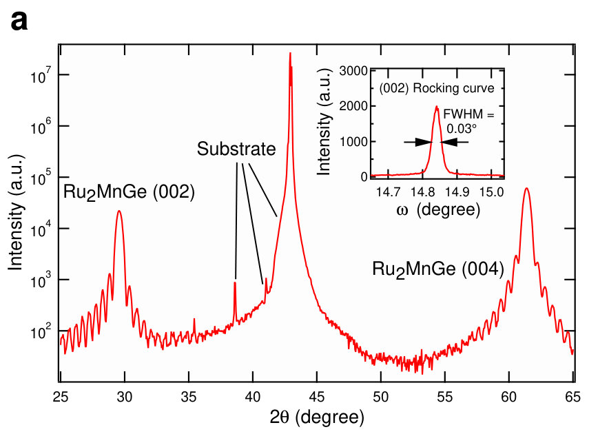 Figure 1
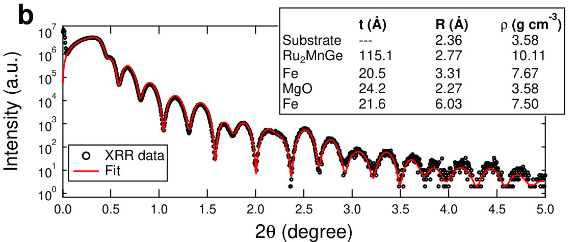 Figure 1
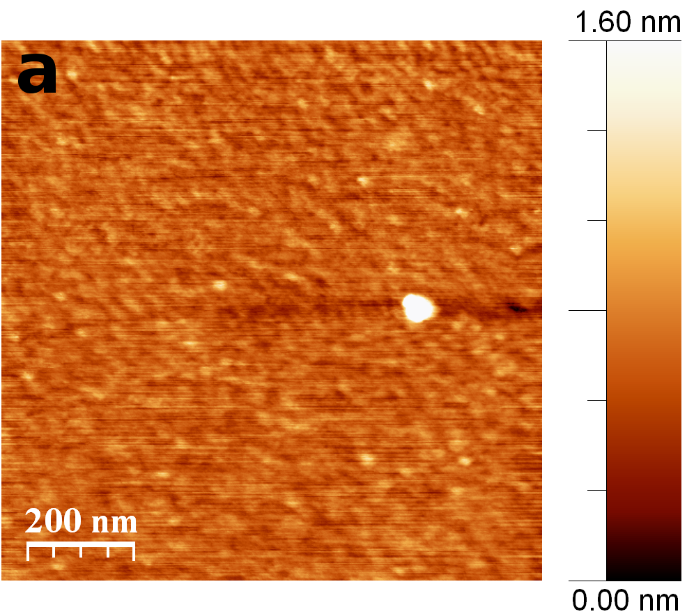 Figure 2
 Figure 2
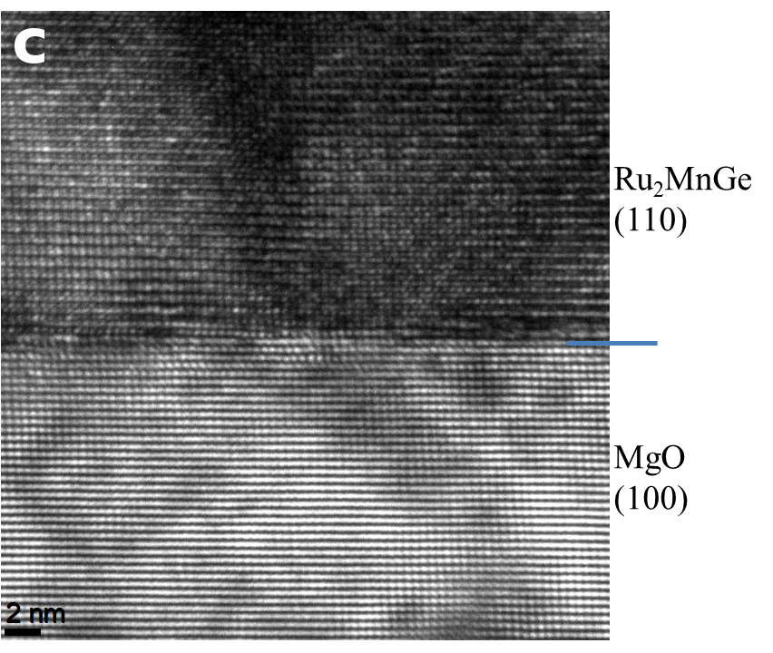 Figure 2
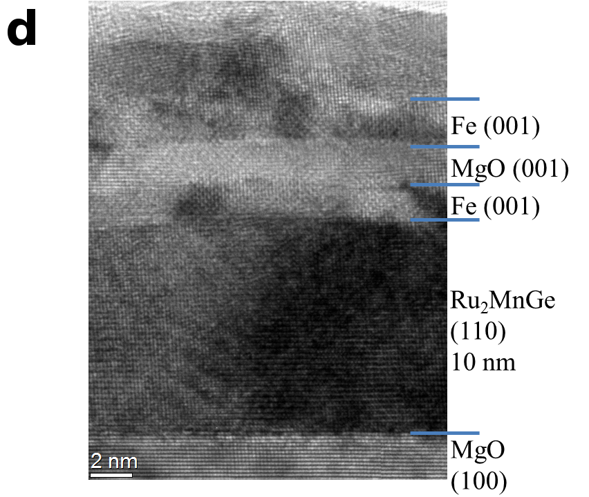 Figure 2
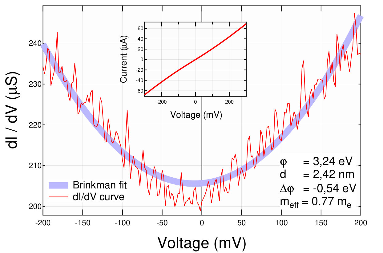 Figure 3
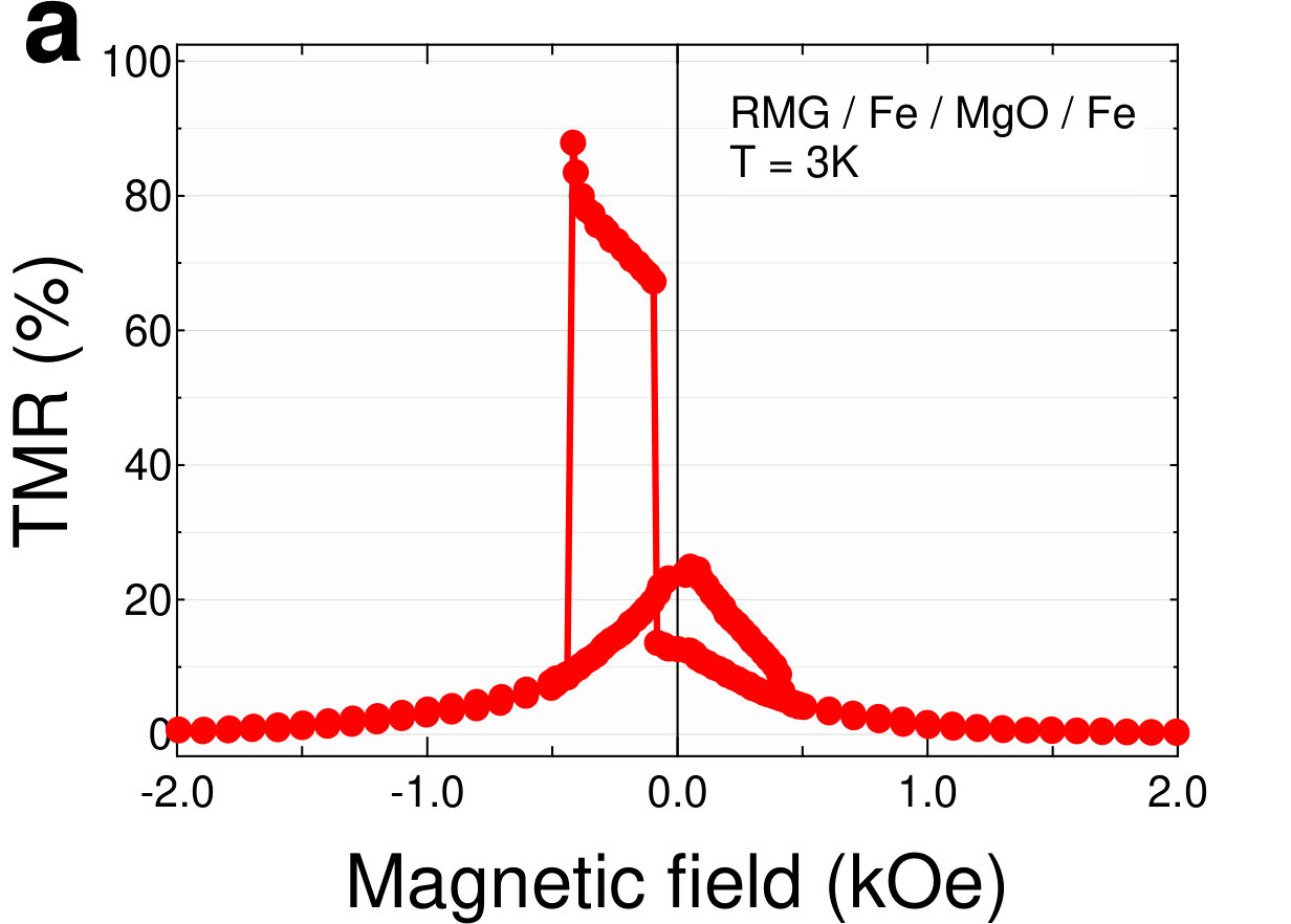 Figure 4
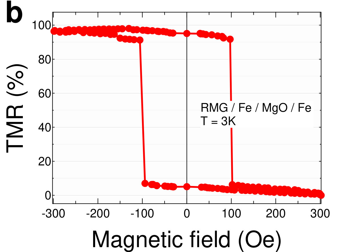 Figure 4
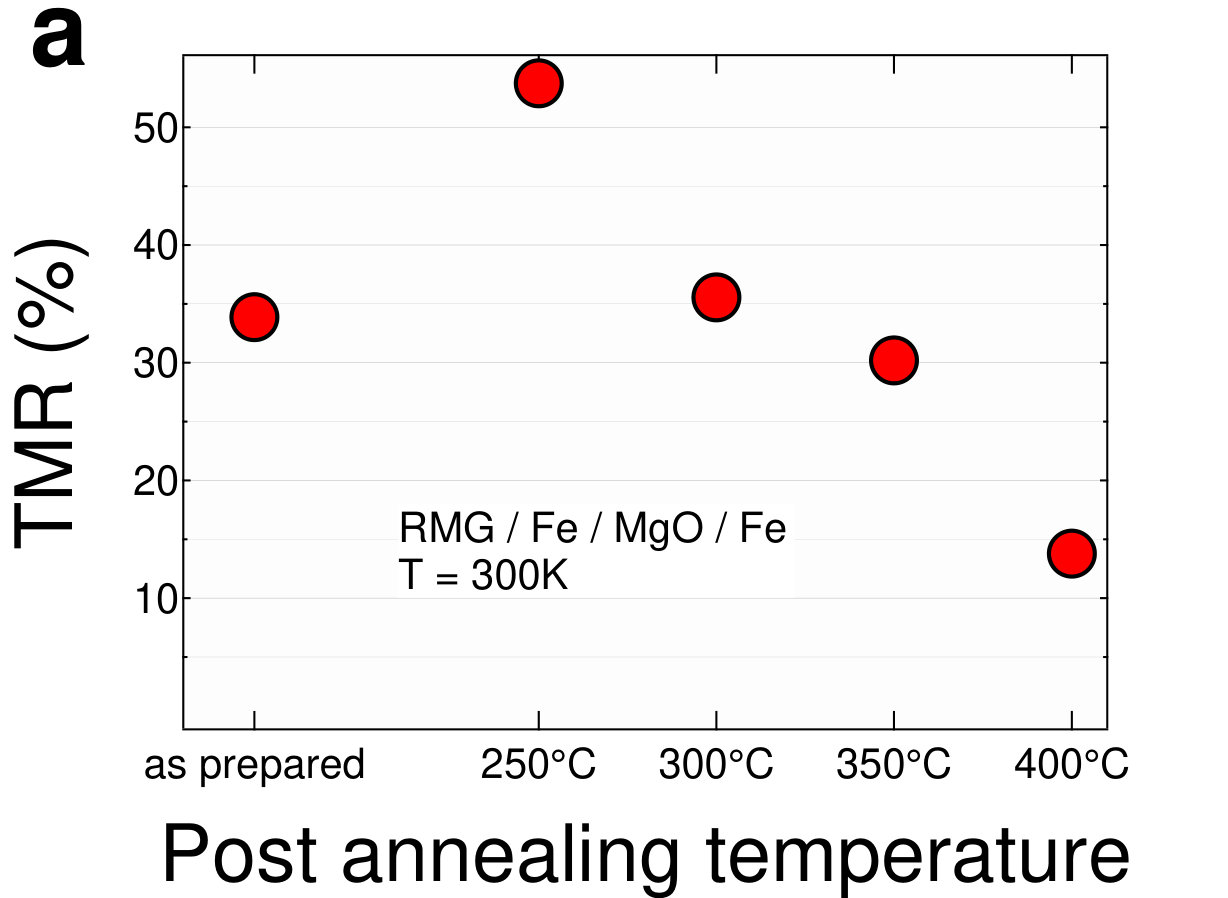 Figure 5
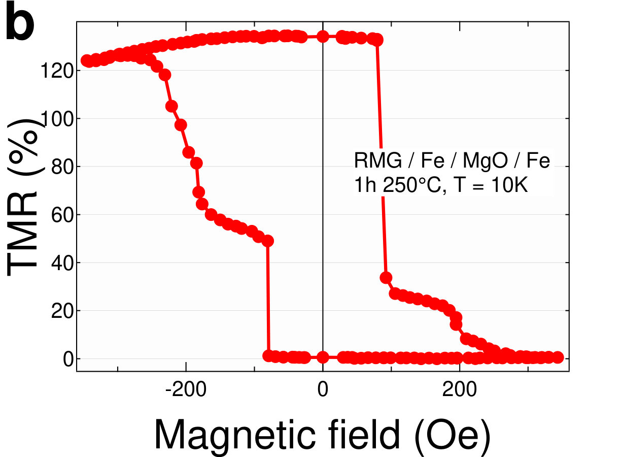 Figure 5
Peer Reviews
No public reviews on file for this paper yet. If you reviewed it on a platform where reviews are public (OpenReview, ICLR, NeurIPS, ICML), you can paste yours below so the community can read it here.
Videos
No videos yet. Explain this paper in a talk, walkthrough, or lecture? Add one.
Integration of antiferromagnetic Heusler compound Ru2MnGe into spintronic devices
Jan Balluff
Center for Spinelectronic Materials and Devices, Bielefeld University, D-33501 Bielefeld, Germany
Teodor Huminiuc
Department of Physics, University of York, York YO10 5DD, England
Markus Meinert
Center for Spinelectronic Materials and Devices, Bielefeld University, D-33501 Bielefeld, Germany
Atsufumi Hirohata
Department of Electronics, University of York, York YO10 5DD, England
Günter Reiss
Center for Spinelectronic Materials and Devices, Bielefeld University, D-33501 Bielefeld, Germany
Abstract
We report on the first integration of an antiferromagnetic Heusler compound acting as a pinning layer into magnetic tunneling junctions. The antiferromagnet Ru2MnGe is used to pin the magnetization direction of a ferromagnetic Fe layer in MgO based thin film tunnelling magnetoresistance stacks. The samples were prepared using magnetron co-sputtering. We investigate the structural properties by X-ray diffraction and reflection, as well as atomic force and high-resolution transmission electron microscopy. We find an excellent crystal growth quality with low interface roughnesses of 1-3 Å, which is crucial for the preparation of working tunnelling barriers. Using Fe as a ferromagnetic electrode material we prepared magnetic tunneling junctions and measured the magnetoresistance. We find a sizeable maximum magnetoresistance value of 135%, which is comparable to other common Fe based MTJ systems.
I Introduction
Antiferromagnets are widely used in spintronics to create a magnetically fixed ferromagnetic reference layer using the exchange bias effect Meiklejohn1956 ; Nogues1999 . The exchange bias effect causes a broadening and a shift of the ferromagnetic layer’s hysteresis loop in the field direction. In combination with an unpinned ferromagnetic layer, magnetoresistive devices like the magnetic tunneling junction (MTJ) are designed. In addition, recently pioneering work on antiferromagnetic spintronics Jungwirth2016 was published, where antiferromagnets are used as an active component in spintronic devices. By exploiting specific symmetry properties of a material a current induced switching of its magnetic state is possible Wadley2016 . Exclusively using an antiferromagnetic material as an active component brings in the advantage of insensitivity to external magnetic fields e.g. for data storage. Thus, antiferromagnets play an important role in the field of spintronics. Especially the widely used antiferromagnetic IrMn or PtMn are, however, costly and rare. In conjunction with the rising field of antiferromagnetic spintronics suitable, novel antiferromagnetic materials are of increasing interest.
Heusler compounds are a ternary material class of the type X2YZ, where the basic crystal structure is a four-atom basis in an fcc lattice (space group Fmm, prototype Cu2MnAl). They are very versatile rendering them interesting for a wide range of applications Graf2011 . Ferro- and ferrimagnetic Heusler compounds are extensively studied Bai2012 as they provide large magnetoresistance ratios Liu2012 in giant or tunnelling magnetoresistance (GMRBaibich1988 ; Binasch1989 and TMRGregg2002 ; Chappert2007 , respectively) devices. However, to the best of our knowledge no work on spintronic devices using an antiferromagnetic Heusler compound as a pinning layer has been reported so far. Due to the matching crystal structure a combination of antiferromagnetic and ferromagnetic Heusler compounds can lead to high quality TMR stacks.
We study the integration of the recently investigated Balluff2015 ; Fukatani2013 antiferromagnetic Heusler compound Ru2MnGe (RMG) into MTJ spin valves. Within our previous work we have already shown that a sizeable exchange bias effect of up to 600 Oe is found in RMG / Fe bilayers Balluff2015 . Furthermore, we measured the blocking temperature, at which the exchange bias vanishes, to be K. Within this work, we prepared RMG based thin film devices using dc and rf magnetron co-sputtering as well as electron beam evaporation. We compare measurements of the thin film roughness and crystal growth quality by using methods of X-ray diffraction (XRD), atomic force microscopy (AFM) and high resolution transmission electron microscopy (HR-TEM). Furthermore, the resulting TMR amplitudes of our devices as a function of different annealing temperatures are investigated to improve effect sizes and especially examine the applicability by an investigation of the tunnelling barrier quality.
II Experimental details
Our RMG layers were prepared using magnetron co-sputtering from elemental targets, where the Ar working pressure is typically mbar during the process. The base pressure of the sputter deposition system is better than mbar. Adjusting the magnetron power allows precise control of the stoichiometry, which was checked using X-ray fluorescence and is typically accurate within 1%at. The RMG layer was sputter-deposited on MgO single crystalline substrates with the epitaxial relation RMG[100] MgO[110]. The lattice mismatch is 0.5%, so no buffer layer was used. The layer was deposited at a substrate temperature of 500∘C. After deposition, the sample was further annealed in-situ at the same temperature for one hour and then cooled down to ambient temperature. A TMR stack in the form of Fe 2 nm / MgO 2 nm / Fe 2 nm was deposited at room temperature. All layers were deposited by magnetron sputtering except the MgO tunneling barrier, which was deposited using an electron beam evaporator with a deposition rate of approximately Å/s. As an electrical contact, a layer of Ta 3 nm / Ru 5 nm was deposited on top of the TMR stack.
In a first step, the samples were analyzed by X-ray reflectivity and diffraction in a Philips X’Pert Pro MPD diffractometer with Bragg-Brentano optics operated with Cu Kα radiation. Further characterization of the samples regarding interface roughness was done using X-ray reflectivity (XRR) and AFM. XRR measurements were done up to and fitted according to the Parratt formalism Parratt1954 . AFM images were recorded using a Bruker Multimode 5 microscope operated in tapping mode. Magnetic analysis of the exchange bias provided by RMG is found elsewhere Balluff2015 .
The tunneling barrier was investigated by cross-sectional HR-TEM using a JEOL JEM-2200FS electron microscope operating at 200kV and equipped with a CEOS image aberration corrector. The samples were prepared by cutting and manually grinding the samples before further processing. The thinned samples were Ar ion milled to electron transparency with a Gatan Precision Ion Polishing System using a temperature controlled stage in order to prevent intermixing at the interfaces.
For the final investigation of MTJ devices the samples were patterned in a standard UV lithography process in combination with secondary ion mass spectroscopy controlled Ar ion beam etching. Square nano pillars of m2 were prepared. The RMG layer is used as a bottom contact for all MTJ cells. Samples were mounted on a chip carrier for electrical measurements and contacted by Au bonding wire using ball and wedge bonding. The magnetoresistance of the TMR devices was measured in a closed-cycle He cryostat.
III Results
The RMG layer shows excellent crystalline growth. The diffraction pattern for a 20 nm thick layer without a TMR stack is shown in in Fig. 1a. Here, the expected (002) and (004) peaks for the Heusler structure are found. Both show pronounced Laue oscillations, which are an indication for homogeneous crystal growth. This is further supported by a narrow rocking curve with a full width at half maximum (FWHM) of (shown in the inset). This value is limited by the divergence of the diffractometer optics. The results obtained by XRR for a RMG / Fe / MgO / Fe TMR stack are plotted in Fig. 1b. Here, the measured data as black dots is shown in conjunction with a fit in red. The fit precisely matches the measured data even up to large angles. The resulting layer thickness as well as roughness and density of the RMG, Fe and MgO layers are given in the graph as well.
As indicated by the XRR and XRD analysis, high quality crystal growth is obtained without the necessity of external sample treatment such as further post annealing. The final fit parameter values as given in Fig. 1b indicate a very low roughness of 2-3 Å for the interfaces. For the upper Fe layer, a slightly increased thickness and lower density is found, which is attributed to the increased roughness of 6 Å.
An AFM image of a full TMR stack’s surface is shown in Fig. 2a. The image shows a smooth sample surface without cluster or island nucleation. The white dot is due to contamination and not attributed to the sample. In Fig. 2b the height distribution across the AFM image is given. The low roughness obtained from the XRR measurements is confirmed by this measurement. Here, we find a RMS roughness of 1.3 Å (the contamination is excluded from this calculation).
Fig. 2c and d show HR-TEM cross section images of the sample. The epitaxial growth of the antiferromagnetic RMG is confirmed via the sharp substrate/Heusler alloy interface as seen in Fig. 2c with no defects observed in the bulk of the material. This agrees with the crystallographic studies done by XRD. In the RMG layer the ordered Heusler structure is visible by the alternating planes of Ru and Mn-Ge. The relation of the unit cell dimensions are as expected for the RMG [110] interface. Fig. 2d shows all layers with atomic smooth growth throughout the whole TMR stack. The MgO tunnel barrier and the two ferromagnetic layers show very good crystalline quality throughout and lattice matched deposition at the bcc Fe (001)/MgO (001)/Fe (001) tunnelling interface. The visible 11-12 atomic layers of MgO correspond to a barrier thickness of Å ( Å) confirming the results obtained by XRR. The slight increase in roughness at the interface between the top Fe layer and capping layer is confirmed as observed in the XRR measurements. This does, however, not affect the quality of the MgO barrier.
We investigated the tunneling magnetoresistance of square nano pillar MTJs. Measuring the I-V characteristic as a function of V at room temperature reveals a working tunneling barrier. Applying a Brinkman fit Brinkman1970 to the numerical derivative allows to determine tunneling barrier height , asymmetry and thickness . The inset in Fig. 3 shows the experimental I-V data. The numerically evaluated curve (thin line) is shown in the main plot of Fig. 3 as well as the Brinkman-fit (thick, shaded line). The effective electron mass is a free parameter in this model. As we know the barrier thickness exactly from XRR and HR-TEM, we adjust to obtain the correct value. The final fit parameters given in Fig. 3 are reasonable considering the MgO band gap of 7.8 eV Taurian1985 .
Due to the low blocking temperature of the RMG / Fe bilayer system, the samples are cooled down in a closed-cycle He cryostat for magnetoresistive characterization. During the cooldown, a magnetic field of 4 T was applied. After cooling down, the magnetoresistance is measured by applying a constant voltage of mV across the MTJ and sweeping the magnetic field parallel to the sample. The corresponding loops are shown in Fig. 4 where the magnetoresistance is plotted against the external magnetic field. and are the resistance values in antiparallel (ap) and parallel (p) states, respectively. In the asymmetric major loop (Fig. 4a), the shifted hysteresis of the exchange biased Fe layer is clearly seen, leading to a distinct switching of the two Fe electrodes. The exchange bias observed in the full structured TMR stacks is reduced by a factor of 2-3 to about 250 Oe compared to the previously investigated RMG / Fe bilayers Balluff2015 . The quality of the switching is limited due to the UV lithography process and the corresponding large size of the nano pillars. The minor loop shown in Fig. 4b, however, shows a nearly perfect square switching. The TMR has a sizeable value of about 100%.
We further investigated the TMR after ex-situ post annealing samples in a vacuum furnace at mbar prior to lithography. The samples were annealed at 250∘C to 400∘C in steps of 50∘C, which are typical post annealing temperatures for TMR spin valves. Samples for post annealing are prepared with a slightly increased thickness (3 nm) of the top Fe electrode. Due to the asymmetry of the two ferromagnetic layers, a comparable measurement of the TMR in the unpinned state at room temperature is possible. Low temperature measurements confirmed that this does not affect the TMR effect size. The TMR values measured at room temperature are compared to the as-prepared sample. The results are shown in Fig. 5a. The highest TMR value is observed for post annealing at 250∘C, whereas for 300∘C we found a TMR value comparable to the as-prepared sample. Any further increase of the annealing temperature led to smaller effect sizes. Thus, we investigated a sample annealed at 250∘C at low temperatures. The exchange bias compared to the as-prepared sample is increased to 380 Oe. A minor loop recorded for this sample is shown in Fig. 5b. We observe a clear enhancement in the TMR amplitude to 135% compared to the unannealed sample. However, multidomain switching is clearly visible in the graph, which is unfavourable for a clean switching of the spin valve. This is induced by the post annealing of the whole layered stack. We explain this by further crystallization effects affecting the grain sizes of the upper Fe electrode, also supported by its increased roughness, as well as Mn diffusion from the RMG layer into the TMR stack.
IV Conclusion
We have successfully demonstrated the first integration of an antiferromagnetic Heusler compound as a pinning layer into magnetic tunneling junctions. Investigation of the sputtered thin film multilayers RMG / Fe MgO / Fe by X-ray techniques revealed an excellent crystalline growth combined with a low roughness. Especially, smooth surfaces can be obtained directly in the sputtering process without the necessity of ex-situ treatment, which is confirmed by AFM measurements. A more detailed insight of the MTJ quality is given by HR-TEM investigations. Here, we find the epitaxial growth of the RMG layer on the MgO substrate without any defects. Also, a good quality tunneling barrier throughout the crystal is found, not affected by interface roughness. Our investigations of the magnetoresistance at low temperatures revealed working MTJ nano pillars with a sharp, square-shaped switching in the minor loop of 100 % signal amplitude. The quality of the switching in the major loop is still subject to improvements and mainly limited to the UV lithography process, which limits the device size. We found a decent increase in signal amplitude to 135 % as well as in exchange bias when annealing samples at 250∘C. The effect amplitudes we obtained in the RMG-based TMR system are comparable to similar Fe / MgO / Fe systems Faure2003 . An ex-situ treatment can improve the TMR effect size. Further investigations will include different electrode materials, which may behave differently under post annealing conditions. Especially, our investigation can establish a basis for ”all-Heusler” MTJs with MgO tunneling barriers. Due to the matching crystal structure and giant effect sizes already found in MTJs using Heusler compounds as an electrode material Liu2012 , this is an appealing future task. All in all, the antiferromagnetic RMG Heusler compound is a promising material due to the ease of fabrication. The compound itself or similar related Heusler compounds may be useful in future applications, or even in the new field of antiferromagnetic spintronics.
V Acknowledgement
The research leading to these results has received funding from the European Union Seventh Framework Programme (FP7/2007-2013) under grant agreement no. NMP3-SL-2013-604398.
The reference list from the paper itself. Each links out to its DOI / PubMed record.
- 1(1) W. H. Meiklejohn, and C. P. Bean, Phys. Rev. 105 , 904 (1957).
- 2(2) J. Nogués, and I. Schuller, J. Magn. Magn. Mater. 192 , 203 (1999).
- 3(3) T. Jungwirth, X. Marti, P. Wadley, and J. Wunderlich, Nat. Nanotechnol. 11 , 231–241 (2016).
- 4(4) P. Wadley et al., Science 351 , 587–590 (2016).
- 5(5) T. Graf, S. S. P. Parkin, and C. Felser, IEEE Trans. Magn. 47 , 367 (2011).
- 6(6) Z. Bai, L. Shen, G. Han, and Y. P. Fen, Spin 02 , 1230006 (2012).
- 7(7) H. X. Liu, Y. Honda, T. Taira, K. I. Matsuda, M. Arita, T. Uemura, M. Yamamoto, Appl. Phys. Lett. 101(13), (2012). H. Liu, H. X. et al., Appl. Phys. Lett. 101 , (2012).
- 8(8) M. N. Baibich, J. M. Broto, A. Fert, F. N. Van Dau, F. Petroff, P. Eitenne, G. Creuzet, A. Friederich and J. Chazelas, Phys. Rev. Lett. 61 , 2472 (1988).