Realization of an atomically thin mirror using monolayer MoSe2
Patrick Back, Aroosa Ijaz, Sina Zeytinoglu, Martin Kroner, Atac, Imamoglu

TL;DR
This paper demonstrates an electrically tunable, atomically-thin mirror using monolayer MoSe2 that achieves high extinction and reflection, with potential applications in optical modulation and optomechanics.
Contribution
The study experimentally realizes a monolayer MoSe2-based mirror with electrical tunability and high reflectivity, advancing 2D material applications in photonics.
Findings
Achieves 90% extinction of resonant incident light.
Maximum reflection coefficient of 45%.
Reflectivity is tunable via gate voltage.
Abstract
Advent of new materials such as van der Waals heterostructures, propels new research directions in condensed matter physics and enables development of novel devices with unique functionalities. Here, we show experimentally that a monolayer of MoSe2 embedded in a charge controlled heterostructure can be used to realize an electrically tunable atomically-thin mirror, that effects 90% extinction of an incident field that is resonant with its exciton transition. The corresponding maximum reflection coefficient of 45% is only limited by the ratio of the radiative decay rate to the linewidth of exciton transition and is independent of incident light intensity up to 400 Watts/cm2. We demonstrate that the reflectivity of the mirror can be drastically modified by applying a gate voltage that modifies the monolayer charge density. Our findings could find applications ranging from fast…
Click any figure to enlarge with its caption.
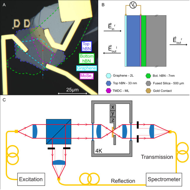 Figure 1
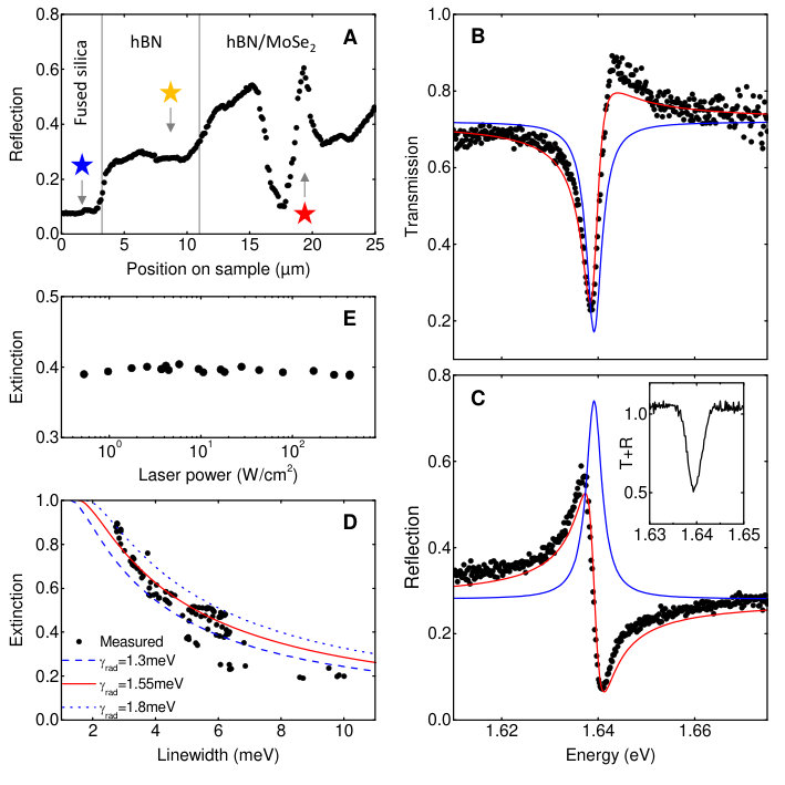 Figure 2
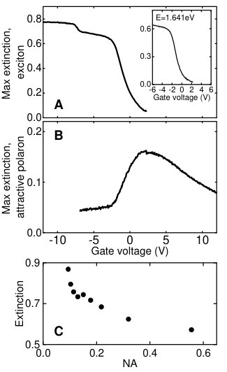 Figure 3
 Figure 4
Peer Reviews
No public reviews on file for this paper yet. If you reviewed it on a platform where reviews are public (OpenReview, ICLR, NeurIPS, ICML), you can paste yours below so the community can read it here.
Videos
No videos yet. Explain this paper in a talk, walkthrough, or lecture? Add one.
Realization of an atomically thin mirror using monolayer MoSe2
Patrick Back,1 Aroosa Ijaz,1 Sina Zeytinoglu,1 Martin Kroner,1∗ Atac Imamoğlu1∗
1Institute for Quantum Electronics, ETH Zürich,
CH-8093 Zurich, Switzerland
∗E-mail: [email protected] or [email protected]
Advent of new materials such as van der Waals heterostructures, propels new research directions in condensed matter physics and enables development of novel devices with unique functionalities. Here, we show experimentally that a monolayer of MoSe2 embedded in a charge controlled heterostructure can be used to realize an electrically tunable atomically-thin mirror, that effects extinction of an incident field that is resonant with its exciton transition. The corresponding maximum reflection coefficient of is only limited by the ratio of the radiative decay rate to the linewidth of exciton transition and is independent of incident light intensity up to Watts/cm2. We demonstrate that the reflectivity of the mirror can be drastically modified by applying a gate voltage that modifies the monolayer charge density. Our findings could find applications ranging from fast programmable spatial light modulators to suspended ultra-light mirrors for optomechanical devices.
A plethora of ground-breaking experiments have established monolayers of transition metal dichalcogenides (TMD) such as MoSe2 or WSe2 as a new class of two dimensional (2D) direct band-gap semiconductors [1, 2, 3, 4, 5]. In the absence of free carriers, the lowest energy elementary optical excitations in TMDs are excitons with an ultra-large binding energy of eV [6]. While encapsulation of TMD monolayers with hexagonal boron nitride (hBN) leads to a reduction of the exciton binding energy [7, 8], it dramatically improves the optical quality, leading to an exciton line-broadening of meV in photoluminescence (PL) or in absorption measurements [9, 10]. Remarkably, these narrow linewidths have a dominant contribution from radiative decay rate; the latter has been determined from exciton-polariton splitting in open cavity structures to be meV for MoSe2 [11, 12]. Motivated by these developments, we previously analyzed the optical response of a monolayer TMD theoretically and showed that it realizes an atomically-thin mirror [13].
Here, we present experiments demonstrating that an hBN encapsulated MoSe2 monolayer has a reflection coefficient exceeding and an extinction of resonant transmitted light of . The combined reflection and transmission measurements allow us to conclude that the fraction of scattered light, stemming from inhomogeneous broadening of the exciton resonance, is less than . Figure 1A shows a micrograph of the charge tunable heterostructure we have studied: a m by m MoSe2 monolayer is sandwiched between two hBN layers. The heterostructure is placed on top of a transparent fused-silica substrate and capped with bilayer graphene. A gate voltage applied between bilayer graphene and the MoSe2 layer allows for tuning the electron density [14, 15] and thereby modifying the resonance frequency as well as the nature of the elementary optical excitations [12].
Figure 1B depicts the outline of our experiments. We use near-resonant light to probe the excitonic excitations. To the extent that the MoSe2 monolayer and its environment is homogeneous, in-plane momentum is a good quantum number for both exciton and radiation field modes. In this limit, we use the input-output formalism of quantum optics to express the outgoing right-propagating electric field mode E (Fig. 1B) in terms of the incident field modes E and E [13]
[TABLE]
where and denote the transition frequency and the radiative decay rate of the excitons. gives the ratio of radiative decay rate to the total (Lorentzian) exciton line broadening . In our experiments whereas ; in this limit the reflected and transmitted fields are given by and , respectively. The minimum and maximum (resonant) intensity transmission and reflection coefficients are given by and . Our formulation does not take into account small asymmetry in radiative decay rates into left and right propagating field modes stemming from the fused-silica substrate.
We measure the transmission and reflection spectrum of the heterostructure in a cryogenic transmission microscope with free space optical access as shown in Fig. 1C. The incident light is focussed to a diffraction limited spot with diameter . For the excitation we use either a broad band light emitting diode (LED) centered at 780nm or a tunable single-mode Ti:S laser. Due to losses on the windows of the cryostat and the finite coupling/detection efficiency we can not directly measure the absolute reflected and transmitted power. Instead, we use a reference reflection and transmission spectrum of the incident light by moving our excitation spot off the MoSe2 layer or off the heterostructure to the fused-silica layer.
Figure 2A shows the intensity reflection coefficient of light with a photon energy of eV as we move the excitation/detection spot along the white line indicated in Fig. 1A. In the region around the blue spot, we measure the reflectivity of fused-silica layer; the extracted reflection coefficient of (see Supplementary Materials) is in good agreement with reflection we would expect from a thick fused-silica layer. Moving to the orange spot where we have the graphene/hBN heterostructure without the MoSe2 monolayer, we observe a sizeable increase in reflection coefficient to about . Finally, reflection of the full heterostructure around the red spot exhibits very large variations in reflection coefficient ranging from to more than , demonstrating the ultra-strong optical response of monolayer MoSe2. Spatial variations in exciton resonance frequency, most likely stemming from inhomogeneous strain profile, result in the observed position dependent reflection coefficient of incident photons at a fixed frequency.
Figure 2B shows the normalized transmission spectrum obtained at the red spot, using a detection path numerical aperture (NA) of . Even though the strong extinction of resonant light is evident, the dispersive nature of the transmission spectrum stemming from optical interference effects, does not allow us to read from the data directly. To extract the maximal extinction, we fit the data with a dispersive Lorentzian model (red curve). We find that a good fit is obtained for meV yielding an extinction coefficient of . We emphasize that extinction factors of this magnitude were previously only reported for transmon qubits coupled to superconducting microwave waveguides [16].
The reflection spectrum corresponding to the transmission data obtained at the red spot is depicted in Fig. 2C. The stronger asymmetry in reflection originates from an optical interference between two contributions with comparable magnitude – the excitonic emission and the incident light reflected from the heterostructure. The parameters used in the dispersive Lorentzian fit (red curve) to the reflection data using the same resonance energy and as for the transmission spectrum, allows us to determine the maximal reflection coefficient of the MoSe2 layer to be . Remarkably, the sum of reflection and transmission, normalized to the corresponding value in the region around the orange spot, yields a symmetric but non-Lorentzian dip at the exciton resonance energy (Fig. 2C inset): the reduction of the total light intensity on resonance is a consequence of non-radiative line broadening and confirms that losses due to scattering into high field modes or due to non-radiative recombination is less than .
The aforementioned spatial inhomogeneity of the exciton resonance results in a variation of not only the exciton resonance energy but also its linewidth across the sample. Figure 2D shows the dependence of the extracted resonant extinction coefficient on the linewidth of the exciton resonance, obtained by measuring transmission at different spots. We find that the broadened lineshapes are reasonably well fit by dispersive Lorentzians allowing us to compare the dependence of maximal extinction on total exciton linewidth ( to the theoretical value . This comparison in turn allows us to determine the radiative decay rate to be in the range meV meV, which is in good agreement with the values previously determined from normal-mode splitting of exciton-polaritons [11, 12]. We remark that at the locations yielding the highest observed extinction factor of , we extract consistently higher values of . However, at these points even the transmission spectrum exhibits strong asymmetry, rendering the extracted values less reliable.
Since the exciton-exciton interactions are proportional to the Bohr radius [17], we would expect strongly bound TMD excitons with nm to have a linear response to the incident field, provided that the induced exciton density cm*-2*. This argument in turn suggests that the response of this atomically-thin mirror should be independent of the incident light intensity provided that Wcm*-2*. To verify this prediction, we used a single-mode Ti:S laser tuned into resonance with the MoSe2 exciton transition and monitored the dependence of extinction on the laser intensity. Figure 2E shows that the extinction indeed remains unchanged as we vary the incident intensity by 4 orders of magnitude from W/cm2 to W/cm2. Verification of the theoretically predicted unusual saturation characteristics of TMD mirrors is likely to require pulsed laser excitation [13].
Due to strong exciton-electron interactions, the nature of elementary optical excitations can be drastically modified by applying that modifies the free electron (or hole) density () in the TMD monolayer [12]. A typical dependent transmission spectrum is shown in Fig. S4 (Supplementary Materials): as is increased a new attractive exciton-polaron resonance that is red detuned by meV with respect to the bare exciton transition emerges. The abrupt blue-shift and broadening of the exciton resonance for V on the other hand can be understood as the transition from a bare exciton into a repulsive-exciton-polaron resonance. In the context of our work, the dependence of the optical response of the MoSe2 monolayer indicates that the atomically-thin mirror can be electrically tuned.
Figure 3A shows the dependence of maximal extinction coefficient obtained at exciton or repulsive-polaron resonance. The increase of minimum transmission from down to is due to a combination of electron-exciton interaction induced line broadening and oscillator strength transfer to attractive-polaron. If we instead focus on the response to incident photons at a specific energy, we find an even sharper drop in extinction from down to upon increasing from V to [math] V, demonstrating electrical control of an atomically-thin mirror (Fig. 3A inset). With low resistance Ohmic contacts to the MoSe2 monolayer, it should be possible to exploit the strong dependence of excitonic response to realize fast switching of mirror transmission/reflection potentially on sub-ns timescales [18].
Due to the aforementioned oscillator strength transfer, maximal extinction at the attractive-polaron resonance first increases to about before decreasing due to line broadening (Fig. 3B). Even though the optical response of the attractive polaron is relatively modest, its strong dependence on the valley polarization of electrons and its large g-factor exceeding 15 [19] render it an excellent candidate for realization of chiral optical devices.
The experiments shown in Fig. 2A-D as well as in Fig. 3A-B have been obtained by focusing the incident light onto a diffraction limited spot using a lens with NA and then collecting the transmitted or reflected light with an NA . This allowed us to monitor the optical response of excitons with . Figure 3C shows the dependence of maximal extinction for several values of the transmission path NA, close to the same spot we used to obtain the data depicted in Fig. 2B. We observe that as we increase transmission NA from to , the extinction drops from down to while the exciton linewidth increases from meV to meV. We attribute this strong NA dependence to electron-hole-exchange interaction induced modification of the exciton spectrum: it has been theoretically predicted that due to this interaction, the p-polarized excitons would have a Dirac-cone-like dispersion, leading to an energy splitting of s- and p-polarized excitons of order meV for [20, 21]. To the best of our knowledge, the NA-dependent increase in linewidth that we report here provides the first direct evidence for this striking theoretical prediction.
The strong optical response of a TMD monolayer as demonstrated in our experiments opens up new avenues for photonics. On the one hand, the combination of ultra-light mass and high reflectivity suggests that these atomically-thin mirrors could revolutionize the performance of optomechanical mass and force sensors. On the other hand, the possibility to drastically modify reflection on ultra-short time scales on sub-wavelength length scales using applied electric fields could open up new perspectives for digital mirror devices or spatial light modulators. Last but not least, the valley degree of freedom of excitons and exciton-polarons can be used to realize chiral mirror devices by introducing a ferromagnetic monolayer next to the optically active TMD layer [22].
Acknowledgments
This work is supported by an ERC Advanced investigator grant (POLTDES), Spin-NANO Marie Sklodowska-Curie Grant Agreement No. 676108 and NCCR QSIT.
See pages - of supplementary.pdf
The reference list from the paper itself. Each links out to its DOI / PubMed record.
- 1[1] B. Radisavljevic, A. Radenovic, J. Brivio, V. Giacometti, A. Kis, Nat. Nanotechnol. 6 , 147 (2011).
- 2[2] A. Splendiani, et al. , Nano Lett. 10 , 1271 (2010).
- 3[3] B. W. H. Baugher, H. O. H. Churchill, Y. Yang, P. Jarillo-Herrero, Nat. Nanotechnol. 9 , 262 (2014).
- 4[4] L. Britnell, et al. , Science 340 , 1311 (2013).
- 5[5] X. Xu, W. Yao, D. Xiao, T. F. Heinz, Nature Physics 10 , 343 (2014).
- 6[6] A. Chernikov, et al. , Phys. Rev. Lett. 113 , 076802 (2014).
- 7[7] S. Latini, T. Olsen, K. S. Thygesen, Phys. Rev. B 92 , 245123 (2015).
- 8[8] A. V. Stier, N. P. Wilson, G. Clark, X. Xu, S. A. Crooker, Nano Lett. 16 , 7054 (2016).