Negative electronic compressibility enables electrically-induced charge density waves in a two-dimensional electron liquid
Erica E. Hroblak, Alessandro Principi, Hui Zhao, Giovanni Vignale

TL;DR
This paper demonstrates that negative electronic compressibility in 2D electron systems allows for electrically-induced, tunable charge density waves without current flow, controlled by screening length and force magnitude.
Contribution
It introduces a novel mechanism for generating charge density waves in 2D electron liquids via negative compressibility and uniform force fields.
Findings
Charge density waves can be generated without current flow.
Wave properties are tunable by electrical parameters.
Negative compressibility enables new electronic phase control.
Abstract
We show that the negative electronic compressibility of two-dimensional electronic systems at sufficiently low density enables the generation of charge density waves through the application of a uniform force field, provided no current is allowed to flow. The wavelength of the density oscillations is controlled by the magnitude of the (negative) screening length, and their amplitude is proportional to the applied force. Both are electrically tunable.
Click any figure to enlarge with its caption.
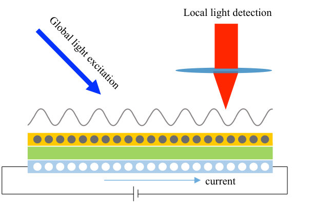 Figure 1
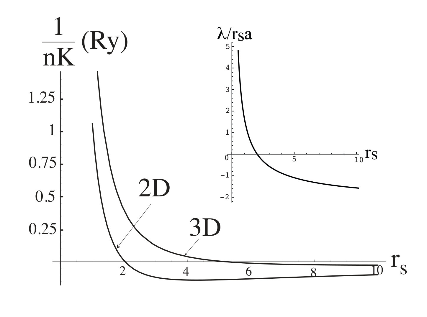 Figure 2
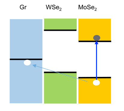 Figure 3
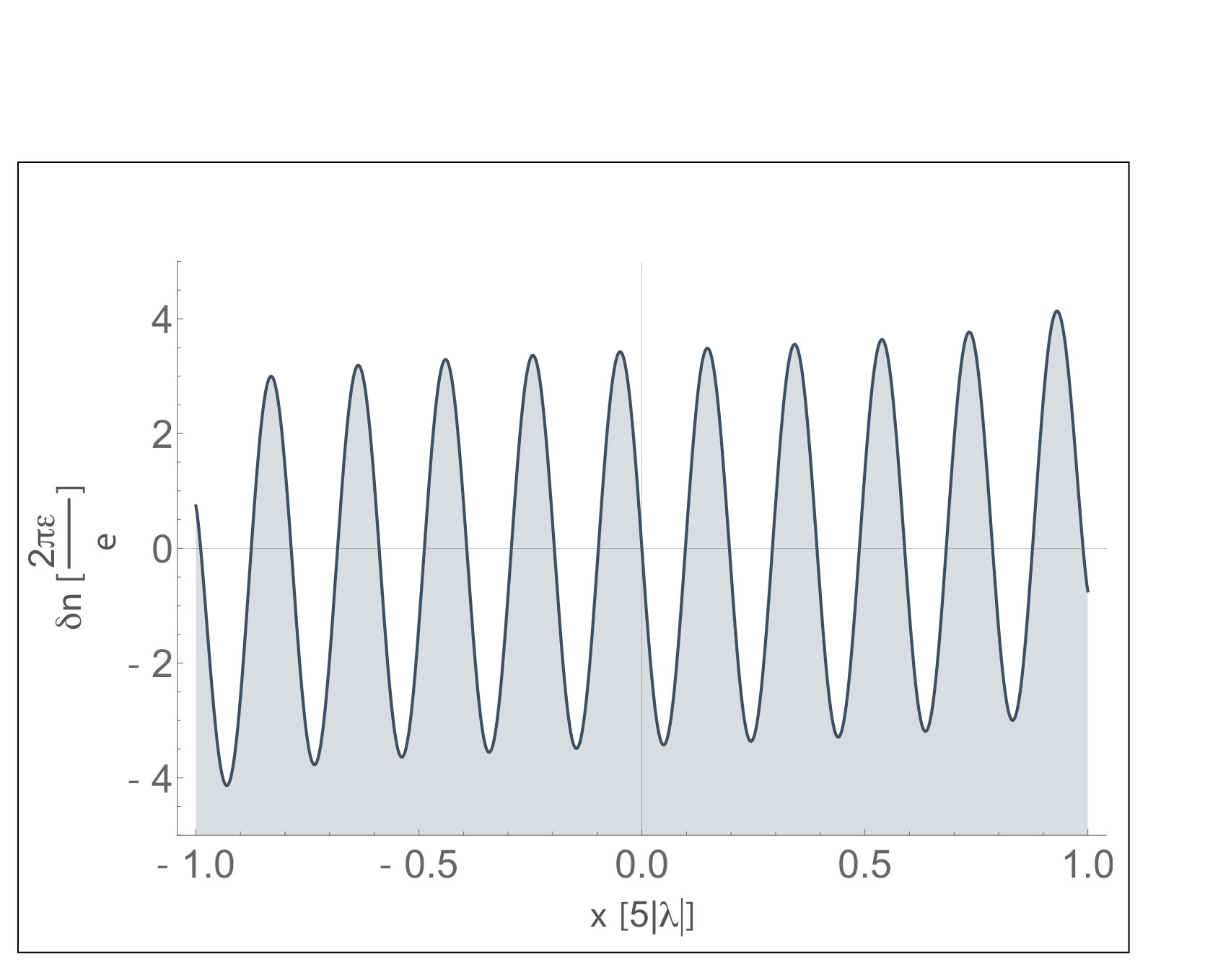 Figure 4
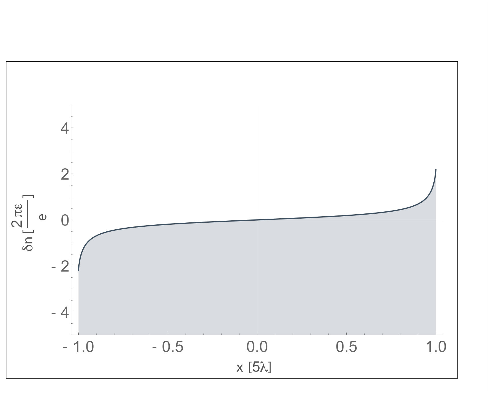 Figure 5
Peer Reviews
No public reviews on file for this paper yet. If you reviewed it on a platform where reviews are public (OpenReview, ICLR, NeurIPS, ICML), you can paste yours below so the community can read it here.
Videos
No videos yet. Explain this paper in a talk, walkthrough, or lecture? Add one.
Negative electronic compressibility enables electrically-induced charge density waves in a two-dimensional electron liquid
Erica E. Hroblak
Department of Physics and Astronomy, University of Missouri, Columbia, Missouri 65211, USA
Alessandro Principi
Radboud University, institute for Molecules and Materials, NL-6525 AJ Nijmegen, The Netherlands
Hui Zhao
Department of Physics and Astronomy, University of Kansas, Lawrence, Kansas 66045, USA
Giovanni Vignale
Department of Physics and Astronomy, University of Missouri, Columbia, Missouri 65211, USA
Abstract
We show that the negative electronic compressibility of two-dimensional electronic systems at sufficiently low density enables the generation of charge density waves through the application of a uniform force field, provided no current is allowed to flow. The wavelength of the density oscillations is controlled by the magnitude of the (negative) screening length, and their amplitude is proportional to the applied force. Both are electrically tunable.
Introduction – The occurrence of negative compressibility is a peculiar feature of electronic systems, whose stability against long-range Coulomb repulsion is ensured by the presence of a background charge, such as ionized atomic cores in metals, ionized dopants, or gates in semiconductors.GV At moderately low density, the chemical potential of the electrons decreases with increasing density, implying a negative compressibility (see Fig. 1). This happens when the negative exchange and correlation contributions to the energy, arising from the electron-electron interaction, dominate over the positive kinetic energy – which is inevitable at sufficiently low density. GV ; Bello ; Kusminskiy ; Skinner ; Steffen In an ordinary system, a negative compressibility would be a sign of instability, leading to collapse or phase separation, but the electron liquid is generally protected against such instabilities by its background charge. It is only at extremely low densities or at very high magnetic fields that non-uniform phases such as the Wigner crystal Wigner or stripe and bubble phases Fogler are expected to occur.
Experimentally, a negative electronic compressibility has been observed as a positive quantum mechanical correction to the classical capacitance of a capacitor, whose plates are two-dimensional electron layers formed in a semiconductor quantum well (GaAs)Eisenstein , a carbon nanotube Ilani , or the interface between two oxides (LaAlO3/SrTiO3) Li . The effect has also been demonstrated in the two-dimensional electron gas at high magnetic field Kravchenko and in graphene, also at high magnetic field Skinner2 . Very recently, the decrease of the chemical potential with increasing density has been directly observed by ARPES spectroscopy in two-dimensional monolayers of WSe2 Riley and quasi-three dimensional spin-orbit correlated materials He , by conductivity measurements in graphene-MoS2 heterostructures, Larentis and by capacitance measurements in graphene-terminated black phosphorous heterostructures. Wu In these experiments the electronic densities are considerably larger than in conventional semiconductor heterostructures, ruling out the spontaneous occurrence of inhomogeneous phases.
In this paper we introduce a new context in which a negative electronic compressibility can be used: the controlled generation of charge density waves. Charge density waves (CDWs) are static oscillations of the conduction charge density.Overhauser ; Thorne They have long been studied as a possible alternative to incoherent single-particle transport.Fukuyama78 ; Lee79 Unfortunately, the very same charge background that allows the compressibility to go negative is a major obstacle to the formation of charge density waves due to the electrostatic energy cost that such waves would incur. However, we will now show that a uniform and steady force applied to the electrons when the compressibility is negative does produce a charge density wave, provided the electrons are not allowed to flow. One way to apply such a steady force is to pass a current through an adjacent electron layer: in this setup, schematically shown in Fig. 2, the force arises from the Coulomb drag effect, whereby momentum is steadily transferred from a current-carrying layer to a non-current-carrying one.Pogrebinski ; Price ; Gramila ; Rojo ; Narozhny Another way to achieve the result is to drive a current in a single layer in the presence of a perpendicular magnetic field and let the Hall effect generate the required force in the direction perpendicular to the current. CDWs not aligned with the applied current can be generated in Coulomb-drag setups in the presence of a magnetic field, or if the passive layer is a gapped topological insulator, as a consequence of the (standard or anomalous) Hall drag effect. Liu_arxiv_2016 In any case the CDW appears when the two-dimensional screening length () is negative, which occurs for (see inset of Fig. 1). The wave vector of the CDW is parallel to the direction of the force, and its wavelength is . Both the amplitude and the wavelength of the CDW can be electrically tuned: the former by changing the applied force, the latter by changing, via a gate, the density of the passive layer, and hence the value of .
Model and its solution – We consider a two-dimensional electron gas of uniform two-dimensional density on an infinite strip of length in the direction. A uniform background of positive charge exactly neutralizes the electron charge. We now assume that a force acts on each electron. In the Coulomb drag set-up of Fig. 2 is proportional, via the transresistance Gramila , to the current that flows in the adjacent layer. We begin by considering the classical equilibrium solution. Because no current can flow in the direction, the external force must be exactly balanced by the electric field that arises from the rearrangement of the charge in the plane. Assuming that the density remains uniform in the direction the equilibrium condition is
[TABLE]
where is the deviation of the two-dimensional electron density from equilibrium. It is natural to express in units of and the density in units of . In these units the solution of Eq. (1) is easily seen to be
[TABLE]
where is the Chebyshev polynomial of order . Notice that this solution does not depend on any microscopic length scale: it simply scales with the geometric size.
As the size of the system decreases, it becomes essential to include the quantum mechanical force arising from the gradient of the chemical potential: {\bf F}_{q}=-\mbox{\boldmath\nabla}\mu. In the local density approximation this is approximated as
[TABLE]
Strictly speaking, the local density approximation is valid when the scale of variation of the density is large in comparison to the average inter particle spacing. While this condition is only marginally satisfied, we will argue in the following that it is nevertheless adequate to predict density oscillations in the 2DEG, provided the wave vector remains smaller than 2, where is the Fermi wave vector. By further assuming that we are in the linear response regime, we evaluate the derivative of at the homogeneous equilibrium density. In terms of the dimensionless screening length,
[TABLE]
the equilibrium condition becomes
[TABLE]
This linear integro-differential equation can be solved numerically by expanding the density in Chebyschev polynomials as follows:
[TABLE]
where only odd polynomials are included, consistent with the symmetry of the problem. We than have
[TABLE]
where is the associated Chebyschev polynomial. Substituting these expressions into Eq. (5), multiplying both sides by , with , and integrating over with the help of standard integrals for the Chebyschev polynomials, we arrive at a set of linear algebraic equations for :
[TABLE]
where
[TABLE]
The solution is
[TABLE]
where denotes the inverse of the matrix , whose matrix elements are given by Eq. (9). The solution is obtained by numerically inverting on a sufficiently large set of Chebyshev polynomials, such that the results become independent of basis size.
The character of the solution depends dramatically on the sign of . When is positive, which is the normal state of affairs when the equilibrium density is high, the correction to the classical solution is hardly observable. The space charge is essentially excluded from the center of the system and accumulates against the edges as expected (Figure 3).
When the equilibrium density is low, however, the exchange and correlation energies overwhelm the kinetic energy Steffen ; Wigner leading to a negative value for . Figure (3) shows the surprising result of the simple change of sign of . Instead of accumulating on the edges as in the classical picture, charges distribute along the width of the layer in a sinusoidal pattern. The amplitude and frequency of these oscillations depend on the applied force, the width of the layer, and the value of , providing ample opportunity for electronic tuning. In the central region of the bar () an analytic solution of the equation can be obtained and it is given by the sum of the classical equilibrium solution and a simple oscillation of wavelength . The details of the analytic solution are supplied in the Appendix. Remarkably, the amplitude of the density oscillations is a non-analytic function of , going as (see Appendix). This means that, for a given magnitude of the force, the amplitude of the density oscillations does not vanish in the mathematically equivalent limits of , or . But while these two limits are mathematically equivalent, their physical significance is entirely different. In the limit , with finite , the local density approximation breaks down due to rapid density variation and the solution is not expected to have a physical significance. Whereas, in the limit of large and finite our solution is expected to be physically meaningful and independent of system size, provided .
In a two-dimensional electron gas the Fermi wave vector is related to the average inter particle distance by GV . Looking at the inset of Fig. 1 we see that the key quantity is never much larger than 1 – rather, it approaches a limiting value in the limit of large . This casts some doubts on the validity of the local density approximation. A more accurate solution of the problem, including full non locality, remains therefore an important issue to be addressed in future work. For the time being, we observe that the static density-density response function of a 2DEG is known to be a fairly constant function of wave vector equal to for all ’s up to (see ref. GV, , Appendix 11). Therefore, to the extent that our solution is a simple oscillation of the density at a single wavelength less than (see Appendix) the use of the local approximation is reasonable for , which is a much weaker condition than .
We conclude with a few comments on the order of magnitude of the predicted CDW and propose a possible experiment to confirm its existence. The order of magnitude of the density modulation is cm*-2* for an electric field of 1 V/m (we assume a dielectric constant for the environment and an effective electron mass approximately equal to the bare mass). Thus for an equilibrium density of order cm*-2* an electric field of order V/m produces a density modulation of the equilibrium density. As for the wavelength of the CDW, a typical value of negative , deduced from Fig. 1, is m.
To realize the Coulomb drag experiment depicted in Fig. 2 we consider a trilayer structure formed by monolayers of MoSe2, WSe2, and graphene, with a band alignment shown in Fig. 5, which is predicted by first-principle calculations Guo2016 and experimentally confirmed Yu2009 . Chemical vapor deposition and mechanical exfoliation techniques to fabricate such van der Waals multilayers are well established Wang2016 ; Ceballos2017 . Steady illumination by a laser beam is used to globally inject electron-hole pairs in MoSe2. The holes transfer to graphene, as dictated by the band alignment, while the electrons remain in MoSe2 due to the energy barrier provided by the middle WSe2 layer. This allows the graphene and MoSe2 layers to be p- and n-doped, respectively, with equal carrier densities, so that global charge neutrality is preserved. For carrier lifetimes of the order of nanoseconds, a carrier density of 1012 cm*-2* is easily achieved.
The large gap exhibited by the MoSe2 layer not only allows to reach large doping concentrations without introducing disorder, but is also beneficial for the realization of the negative compressibility. Indeed, it is well known Kotov2012 that in 2D semimetals, such as graphene, the compressibility does not becomes negative because of the positive contribution of the completely-filled valence band. In contrast to this, in MoSe2 the large gap allows the contribution of the conduction band to dominate and to change the sign of the compressibility for sufficiently low carrier concentration.
By applying a voltage of 10 V over a 10 m graphene channel, with a room temperature mobility of 104 cm2/(V.s) Geim2013 a hole current density of 103 A/m is generated in a m-wide layer. The target Coulomb drag potential of V/m in the MoSe2 electron layer requires a Coulomb drag transresistivity of 102 ohm. Such a value of the transresistivity seem to be realizable in van der Waals heterostructures Geim2013 , in which the distance between the layers is only a few Angstroms. Indeed, values of the transresistivity of the order of 50 ohm have been observed in experiments on bilayer graphene at temperatures of 240 K.Gorbachev2012 The system we propose is expected to support larger transresistivity due to the larger effective mass and consequently higher density of states of electrons in MoSe2. To evaluate the feasibility of optical detection of such a CDW, we note that in MoSe2 a carrier density on the order of 1012 cm*-2* changes the absorption coefficient by 10*-3* at the excitonic resonance. Kumar2014 With proper modulation techniques, it has been demonstrated that a differential absorption (relative change of the absorption coefficient) of the order of 10*-7* can be detected. Cui2015 A 1% CDW amplitude would yield a differential absorption signal of the order of 10*-5*, which is two orders of magnitude higher than the detection sensitivity. For a CDW with a wavelength of the order of 1 m, a direct imaging of the differential absorption can resolve the carrier density modulation. For shorter wavelength CDW, such as 100 nm, a spatial derivative technique can be used Werake2011 . Alternatively, diffraction of a light from the formed grating can be used to detect the CDW.
The innovative experimental setup we propose offers several advantages with respect to standard ones based on semiconductor quantum wells and graphene heterostructures. First of all, the “doping by illumination” method has the advantage of keeping the system clean and free of metallic gates and other external sources of screening, thereby enhancing both the drag transresistivity and the negative contribution to the compressibility. Moreover, the detection method allows to follow the evolution of the CDW wavelength with the density of carriers, allowing to distinguish the non-equilibrium CDW from other phenomena such as Friedel oscillations.
Acknowledgments– We acknowledge support from NSF Grants DMR-1406568 (GV) and DMR-1505852 (HZ). One of us (GV) is indebted to Boris Shklovskii for many insightful comments and suggestions.
Appendix A Appendix: Analytic solution of Eq.(5)
After expressing the density modulation as
[TABLE]
the equation (5) for takes the form
[TABLE]
where the integral is understood in the principal value sense. We seek a solution in the form
[TABLE]
where . Making use of the identity
[TABLE]
we rewrite the first term on the left hand side of Eq.(5) as
[TABLE]
and our equation for becomes
[TABLE]
In the region this simplifies to
[TABLE]
which is expressed in terms of the sine integral function, , as follows:
[TABLE]
This equation requires
[TABLE]
For a solution exists only if is negative and
[TABLE]
Thus, the correction to the classical solution is
[TABLE]
In the limit we have
[TABLE]
yielding
[TABLE]
Observe the strong non-analyticity of the solution for . While the wavelength of the density oscillations shrinks to zero, the derivative grows so that the amplitude remains constant in the limit. As discussed in the main text, the limit is unphysical if interpreted as at finite system size , but has a clear physical significance for finite and , where it describes finite amplitude oscillations in a system of infinite size.
The reference list from the paper itself. Each links out to its DOI / PubMed record.
- 1(1) G. F. Giuliani & G. Vignale Quantum theory of the electron liquid (Cambridge University Press, 2005), Chapter 5.
- 2(2) M. S. Bello, E. I. Levin, B. I. Shklovskii, and A. L. Efros, Sov. Phys. JETP, 53(4) 822 (1981).
- 3(3) S. V. Kusminskiy, J. Nilsson, D. K. Campbell, & A. H. Castro Neto, Phys. Rev. Lett. 100 , 106805 (2008).
- 4(4) B. Skinner & B. I. Shklovskii, Phys. Rev. B 82 , 155111 (2010).
- 5(5) K. Steffen, R. Frésard, & T. Kopp, Phys. Rev. B 95 , 035143 (2016).
- 6(6) E. Wigner, Phys. Rev. 46 , 1002 (1934).
- 7(7) Michael M. Fogler, Stripe and bubble phases in quantum Hall systems; in High Magnetic Fields: Applications in Condensed Matter and Spectroscopy (Springer, Berlin, 2002), pp. 98-138.
- 8(8) J. P. Eisenstein, L. N. Pfeiffer, & K. W. West, Phys. Rev. Lett. 68 , 674 (1992).