Giant spin-splitting and gap renormalization driven by trions in single-layer WS$_2$/h-BN heterostructures
Jyoti Katoch, S{\o}ren Ulstrup, Roland J. Koch, Simon Moser, Kathleen, M. McCreary, Simranjeet Singh, Jinsong Xu, Berend T. Jonker, Roland K., Kawakami, Aaron Bostwick, Eli Rotenberg, Chris Jozwiak

TL;DR
This study demonstrates that electron doping in single-layer WS$_2$/h-BN heterostructures causes giant spin-splitting and band gap renormalization due to trion formation, revealing tunable electronic and spintronic properties in 2D materials.
Contribution
It reveals the significant impact of trions on spin-orbit splitting and band gap in 2D heterostructures, a novel insight into many-body effects in these systems.
Findings
Giant renormalization of spin-orbit splitting from 430 meV to 660 meV.
Band gap reduction of at least 325 meV upon doping.
Trionic quasiparticles significantly influence electronic properties.
Abstract
In two-dimensional (2D) semiconducting transition metal dichalcogenides (TMDs), new electronic phenomena such as tunable band gaps and strongly bound excitons and trions emerge from strong many-body effects, beyond spin-orbit coupling- and lattice symmetry-induced spin and valley degrees of freedom. Combining single-layer (SL) TMDs with other 2D materials in van der Waals heterostructures offers an intriguing means of controlling the electronic properties through these many-body effects via engineered interlayer interactions. Here, we employ micro-focused angle-resolved photoemission spectroscopy (microARPES) and in-situ surface doping to manipulate the electronic structure of SL WS on hexagonal boron nitride (WS/h-BN). Upon electron doping, we observe an unexpected giant renormalization of the SL WS valence band (VB) spin-orbit splitting from 430~meV to 660~meV, together…
Click any figure to enlarge with its caption.
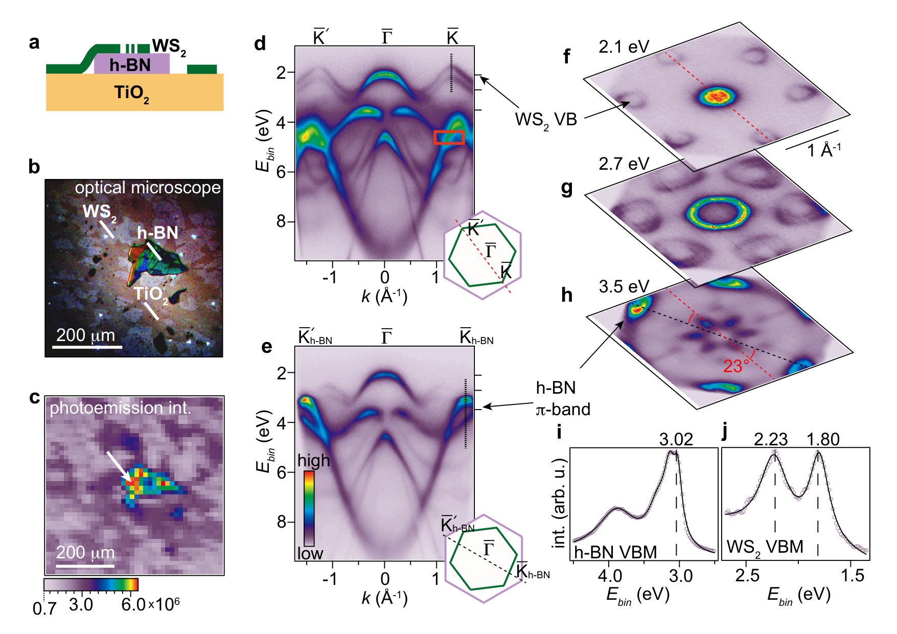 Figure 1
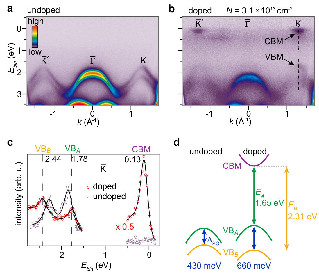 Figure 2
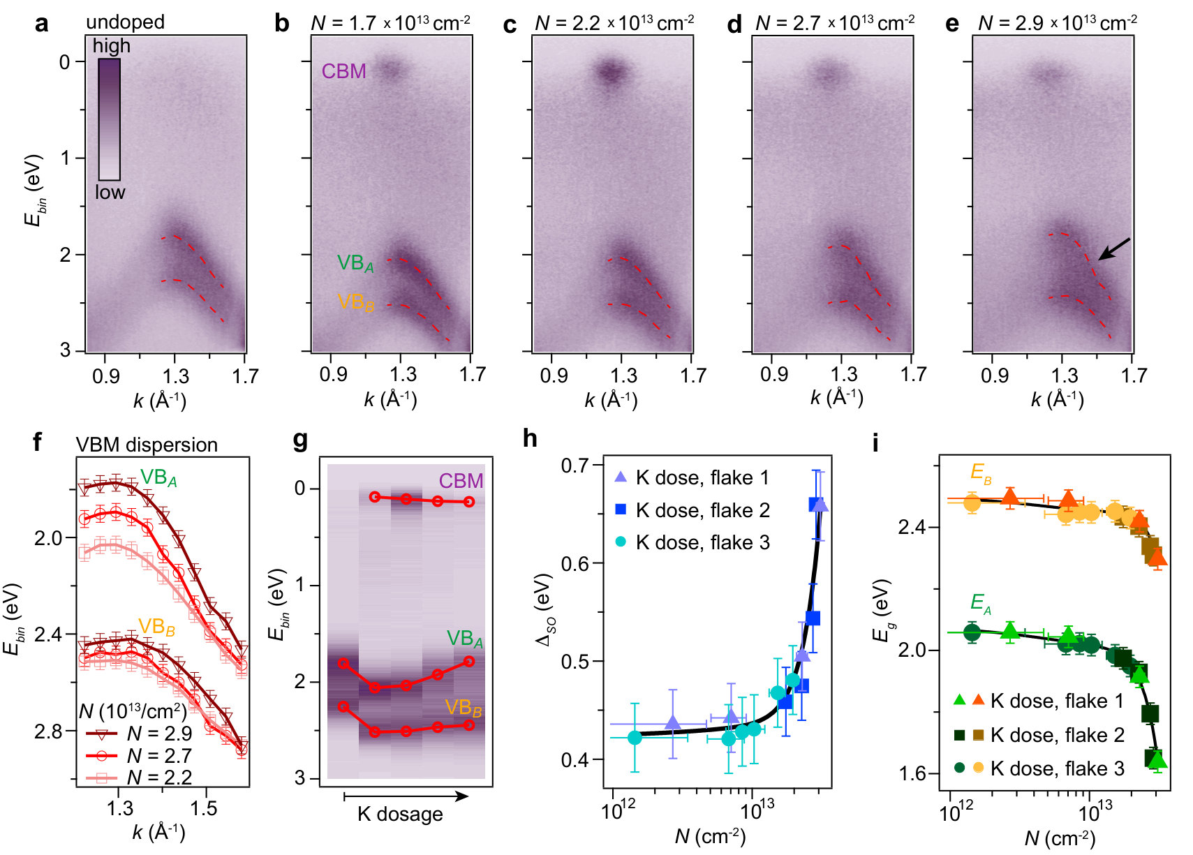 Figure 3
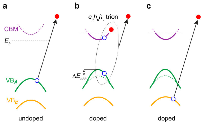 Figure 4
Peer Reviews
No public reviews on file for this paper yet. If you reviewed it on a platform where reviews are public (OpenReview, ICLR, NeurIPS, ICML), you can paste yours below so the community can read it here.
Videos
No videos yet. Explain this paper in a talk, walkthrough, or lecture? Add one.
Giant spin-splitting and gap renormalization driven by trions in single-layer WS2/h-BN heterostructures
Jyoti Katoch*∗*
Department of Physics, The Ohio State University, Columbus, Ohio 43210, USA
Søren Ulstrup*∗*
Advanced Light Source, E. O. Lawrence Berkeley National Laboratory, Berkeley, California 94720, USA
Department of Physics and Astronomy, Interdisciplinary Nanoscience Center (iNANO), Aarhus University, 8000 Aarhus C, Denmark
Roland J. Koch
Advanced Light Source, E. O. Lawrence Berkeley National Laboratory, Berkeley, California 94720, USA
Simon Moser
Advanced Light Source, E. O. Lawrence Berkeley National Laboratory, Berkeley, California 94720, USA
Kathleen M. McCreary
Naval Research laboratory, Washington, D.C. 20375, USA
Simranjeet Singh
Department of Physics, The Ohio State University, Columbus, Ohio 43210, USA
Jinsong Xu
Department of Physics, The Ohio State University, Columbus, Ohio 43210, USA
Berend T. Jonker
Naval Research laboratory, Washington, D.C. 20375, USA
Roland K. Kawakami
Department of Physics, The Ohio State University, Columbus, Ohio 43210, USA
Aaron Bostwick
Advanced Light Source, E. O. Lawrence Berkeley National Laboratory, Berkeley, California 94720, USA
Eli Rotenberg
Advanced Light Source, E. O. Lawrence Berkeley National Laboratory, Berkeley, California 94720, USA
Chris Jozwiak†
Advanced Light Source, E. O. Lawrence Berkeley National Laboratory, Berkeley, California 94720, USA
∗ These authors contributed equally to the work.
† Email: [email protected]
In two-dimensional (2D) semiconducting transition metal dichalcogenides (TMDs), new electronic phenomena such as tunable band gaps Chernikov et al. (2015a); Liang and Yang (2015); Chernikov et al. (2015b) and strongly bound excitons and trions emerge from strong many-body effects Ramasubramaniam (2012); Qiu et al. (2013); Mak et al. (2013), beyond spin-orbit coupling- and lattice symmetry-induced spin and valley degrees of freedom Xiao et al. (2012). Combining single-layer (SL) TMDs with other 2D materials in van der Waals heterostructures offers an intriguing means of controlling the electronic properties through these many-body effects via engineered interlayer interactions Geim and Grigorieva (2013); Ugeda et al. (2014); Larentis et al. (2014). Here, we employ micro-focused angle-resolved photoemission spectroscopy (microARPES) and in-situ surface doping to manipulate the electronic structure of SL WS2 on hexagonal boron nitride (WS2/h-BN). Upon electron doping, we observe an unexpected giant renormalization of the SL WS2 valence band (VB) spin-orbit splitting from 430 meV to 660 meV, together with a band gap reduction of at least 325 meV, attributed to the formation of trionic quasiparticles. These findings suggest that the electronic, spintronic and excitonic properties are widely tunable in 2D TMD/h-BN heterostructures, as these are intimately linked to the quasiparticle dynamics of the materials Xu et al. (2014); Kormányos et al. (2015); Mak and Shan (2016).
Coulomb interactions in 2D materials are several times stronger than in their 3D counterparts. In 2D TMDs, this is most directly evidenced by the presence of excitons with an order of magnitude higher binding energies than in the bulk Ramasubramaniam (2012). While the excitons in these 2D materials have been widely studied by optical techniques Mak and Shan (2016), the impact of strong electron-electron interactions on the quasiparticle band structure remains unclear. Theory predicts many-body effects to influence the spin-orbit splitting around the valence band maximum (VBM) and conduction band minimum (CBM) Ferreiros and Cortijo (2014). While these should be observable by ARPES, a direct probe of many-body effects Bostwick et al. (2007), measurements so far have mainly focused on the layer-dependence of the single-particle spectrum and the direct band gap transition in 2D TMD systems, including epitaxial SL MoSe2 Zhang et al. (2014) and SL WSe2 Zhang et al. (2016) grown on doped multilayer graphene, and SL MoS2 grown on a metal surface Miwa et al. (2015). On such conductive substrates the interfacial interactions and screening are known to strongly influence the electronic properties of the SL TMD Ugeda et al. (2014).
Flakes of SL TMDs have been transferred on oxide substrates such as SiO2 where the substrate screening and interfacial effects are potentially reduced. However, resulting ARPES spectra have been too broad for detailed analysis Jin et al. (2013), likely due to large surface roughness and charge impurity scattering Dean et al. (2010). With respect to SiO2 and similar substrates, h-BN has favorable qualities like atomic flatness, modest screening and a homogeneous charge distribution. This should enable direct investigation of the adjacent TMD’s intrinsic electronic structure and many-body effects. h-BN is often used as a substrate for graphene heterostructures Dean et al. (2010); Geim and Grigorieva (2013) with high device performance Wang et al. (2013) and new exotic electronic states such as quantized Dirac cones Wang et al. (2016). Unfortunately, the lateral size of mechanically assembled heterostructures is usually on the order of m, much smaller than the beam spot of typical ARPES setups (100 m). Furthermore, sample charging on insulating bulk h-BN substrates would complicate ARPES experiments.
We overcome these challenges as follows. We realize a high quality 2D semiconductor-insulator interface by mechanical transfer of a relatively large (100 m) SL WS2 crystal over a thin flake of h-BN that was transferred onto a degenerately doped TiO2 substrate, as depicted in Fig. 1(a). Sample charging is avoided by electrically contacting the continuous SL WS2 flake to both the h-BN and the conductive TiO2. Fig. 1(b) is an optical microscope image of the sample, including a m wide h-BN flake, surrounded by several transferred flakes of SL WS2 on the TiO2 substrate (WS2/TiO2), one of which partially overlaps the h-BN.
By using a state-of-the-art spatially-resolved microARPES experiment with a 10 m focused synchrotron beam spot, we are able to collect distinct high quality band structure information from the multiple micron-scale interfaces. A spatial map of the photoemission intensity around the WS2/h-BN heterostructure is shown in Fig. 1(c), which was produced by integrating the intensity over the boxed region of the corresponding -space band structure shown in Fig. 1(d), measured at each spatial point. The crossing SL WS2 and h-BN bands in this region ensure strong contrast between WS2/h-BN (white arrow), regions of WS2/TiO2 (light purple), and regions of bare TiO2 (dark purple) in the spatial map. The photoemission map (panel (c)) corresponds directly to the optical micrograph (panel (b)) with contrasts that reflect the intensity of the WS2 and h-BN features in the red box in panel (d). The band structures from bare TiO2, WS2/TiO2 and several spots within the WS2/h-BN heterostructure are presented in Supplementary Figure S1. The slight intensity variations within the WS2/h-BN heterostructure arise from areas with pinholes introduced in the SL WS2 during transfer, as sketched in Fig. 1(a) Ulstrup et al. (2016). The sensitivity towards such features, which are not resolved by the optical micrograph, demonstrates the capability of identifying optimum sample areas directly in the ARPES experiment, which is critical for such complex, heterogenous samples.
The VB electronic structure through the entire first Brillouin zone (BZ) of the heterostructure, including the SL WS2 bands and the -band dispersion of the underlying h-BN, is shown in Figs. 1(d)-(e). The data is collected from a single spatial point where the WS2 features are most intense (white arrow in Fig. 1(c)). Custom electrostatic deflectors mounted in the photoelectron analyzer enable full scans of -space at exactly this position without any drift from sample motion. The BZ orientations and twist angle between the two materials are determined from the constant binding energy cuts shown in Figs. 1(f)-(h). From the relative orientation of the hole pockets, we estimate a twist angle of (23 1)∘. The energy distribution curves (EDCs) in Fig. 1(i)-(j) track the VBM binding energy positions of the two materials. The upper VB of SL WS2 is located inside the band gap of h-BN and the SL WS2 VBM is characterized by a spin-orbit splitting of 430 meV (see Fig. 1(j)), in agreement with theoretical predictions Kormányos et al. (2015) and previous experiments Dendzik et al. (2015); Ulstrup et al. (2016). The clear electronic states and lack of band hybridization reveal a weak interlayer interaction between the two materials. Similar to work on graphene/h-BN Wang et al. (2016), we expect these data to represent the intrinsic electronic structure of SL WS2 with negligible substrate influence.
The impact of electron doping on the electronic structure via in-situ surface potassium deposition is shown in Fig. 2(a,b) (see Supplementary Figure S2 for core level data on clean and potassium dosed samples). Doping WS2/h-BN leads to the CBM being populated at the points of SL WS2, confirming the expected direct band gap. A surprising change of the dispersion of the two spin-orbit split bands VBA and VBB of WS2/h-BN around the point is observed, highlighted in the EDCs in Fig. 2(c). The spin-splitting due to spin-orbit coupling increases from 430 meV in the undoped case to 660 meV in the electron-doped case, as sketched in Fig. 2(d). Such a large spin-splitting has not previously been observed in any SL material to our knowledge. In this case, the band gap of SL WS2 is 1.65 eV and the CBM to VBB offset is 2.31 eV. These values are sketched in Fig. 2(d) and denoted as and , respectively, due to the relation with the A and B exciton lines observed in optical experiments Qiu et al. (2013).
A detailed evolution of the band extrema with increasing doping is shown in Fig. 3(a-e). The dispersions around the VBM as determined from EDC line shape analysis (see Supplementary Figure S6) are shown by dashed red curves and directly compared in panel (f). We estimate the charge carrier density, , at each dosing step from the CBM position (see methods). These estimated doping levels are consistent with those achieved in similar experiments on bulk WSe2 Riley et al. (2015) and with the intensity of the potassium 3p core level (see Supplementary Figure S3).
From EDC peak positions at (see Supplementary Figure S7), we extract the VBM and CBM energies as a function of dosing (panel (g)). After the first dosing step ( cm*-2*), the CBM becomes occupied and VBA and VBB rigidly shift to higher binding energy. With further dosing, the CBM moves further down to higher binding energy, while VBA and VBB shift back towards lower binding energy, resulting in a continuous narrowing of the band gap. In particular, the dispersion of VBA appears to renormalize with increased doping (see panels (d,e,f)), with a dramatic increase in (panels (g,h)). This leads to a corresponding change in the relative energy separation between and (panel (i)), implying that the energies of the A and B exciton lines also separate. The data points with different marker shape and color in panels (h,i) stem from separate doping experiments on the three different flakes studied in Fig. 2, Fig. 3 and in Supplementary Figure S8. A reproducible trend is found across all flakes. Note also that in the carrier density range between cm*-2* and cm*-2* we find a more modest band gap renormalization of (90 30) meV, which is in excellent agreement with gated device measurements on a similar sample Chernikov et al. (2015a). Our observations reveal that it is insufficient to only consider rigid band shifts, and that strong dispersion changes can result from doping of SL TMDs.
The surprising doping-induced changes in are likely not directly related to the surface potential induced by the potassium deposition (through, e.g., the Rashba interaction) which is not expected to affect at for SL TMDs. This rather introduces a splitting at , which we do not observe Yuan et al. (2013); Shanavas and Satpathy (2015). Furthermore, we can rule out any potassium induced structural symmetry breaking in our heterostructure, as only minor rigid binding energy shifts of the S 2p core levels of WS2 and of the underlying h-BN -band are observed after complete doping (see Supplementary Figures S4-S5). The reproducible charge carrier dependence of the spectral changes demonstrated in Figs. 2-3 and Supplementary Figure S8 suggest that these changes originate from Coulomb interactions around the band extrema of SL WS2 Chernikov et al. (2015a); Liang and Yang (2015); Ferreiros and Cortijo (2014).
The linewidths of the VBA and CBM peaks exhibit a non-monotonic dependence with doping, which can not be described by simple scattering on ionized potassium impurities (see further discussion in Supplementary Section 4). Specifically, the observation that VBA renormalization coincides with occupation of the CBM suggests that the renormalization is caused by new scattering channels available upon occupation of the conduction band (CB). Previous works utilizing surface potassium deposition for electron-doping of SL TMDs on conductive substrates Zhang et al. (2014, 2016); Miwa et al. (2015) have shown no such changes in , where the Coulomb interactions are already strongly screened in the undoped case Ugeda et al. (2014). We believe that the reduced dielectric constant of the h-BN substrate plays a key role for these observations as it leads to reduced screening of the many-body interactions in the bare SL WS2.
An alkali-atom-induced renormalization of the VB edge at K towards , observed in several bulk TMDs, has been attributed to the breaking of the outermost layers’ degeneracy by the doping-induced field Riley et al. (2015); Kang et al. (2017). This can either be a single-particle effect Kang et al. (2017) or a combination of single- and many-body effects Riley et al. (2015), the latter of which suggests a negative electronic compressibility (NEC), the motion of the chemical potential towards the VBM, i.e. .
In contrast, we observe distinctive effects in SL WS2/h-BN, namely 1) a renormalization of within the single layer, 2) an NEC in which is significantly larger than in the bulk Riley et al. (2015); Kang et al. (2017), and 3) the VBA slope is discontinuous at k=($$\bar{\mathrm{K}}, ′0.15 Å*-1* in Fig. 2(b) at high doping. This leads to kinks in VBA, exemplified by the arrow in Fig. 3(e), which develop continuously in strength with doping in Figs. 3(a)-(e). Such kinks are common in ARPES when the created “photohole” interacts strongly with well-defined (in energy and/or momentum) excitations Bostwick et al. (2007).
As noted above, the band renormalization coincides with the occupation of the CB, suggesting that such excitations are associated with electron-hole (-) pairs near in the CB, induced in response to the VB hole created during photoemission. In the undoped situation sketched in Fig. 4(a) such interactions are not possible. At high carrier densities where the CB is occupied an - excitation around (or ′) can interact with the VB photohole, forming a positively charged, bound electron-hole-hole complex denoted as , where denotes charges in the (CB,VB), respectively, as illustrated in Fig. 4(b). Such a process would renormalize the bare band dispersion and lifetime of the VB states, broadening and shifting their spectra as observed.
These excitations may be compared to the () trions found in - ()-doped TMDs with configuration (). Such trions have been invoked to interpret additional spectral lines shifted in energy by 20-60 meV with respect to the main A exciton line in optical absorption Mak et al. (2013) and luminescence Mak et al. (2013); Zhu et al. (2015) measurements of SL TMDs. Our measurements show a relative shift of VBA by 0.23 eV compared to VBB, which reflects the absolute binding energy reduction of the photohole associated with the formation of the trion (see Fig. 4(b)). The order of magnitude of is compatible with the absolute trion binding energies that can be extracted from the optical experiments Mak et al. (2013); Zhu et al. (2015), however, the exact values are expected to depend on the dielectric environment of the sample and the doping. So far, corresponding trion features associated with B excitons have not been observed in optical experiments, which is fully consistent with the absence of renormalization of the VBB dispersion in the present ARPES data, as seen in Figs. 3(a)-(e) and as sketched in Fig. 4(c). This lack of renormalization of the VBB dispersion might be attributed to additional decay channels of the VBB hole such as decay into the VBA band. The dramatic increase of and the band gap renormalization can therefore be viewed as direct consequences of forming trionic quasiparticles around the VBA and CB extrema.
The assignment of trions in optical measurements of semiconducting TMDs is currently being debated, as a recent theoretical study points towards the possibility of interactions between - pairs and the remaining charge density forming other types of quasiparticles such as exciton-polarons Efimkin et al. (2017). Our ARPES measurements provide direct evidence for such multi-component excitations in SL TMDs and gives access to both their energy and momentum dependence that is lacking from momentum-integrating transport, optical, or tunneling measurements. We envision further theoretical and experimental studies to disentangle such many-body effects in the spectral function of SL TMDs. The charge carrier dependent electronic band gap and spin-splitting that arise from these many-body effects will profoundly impact the charge-, spin- and valley-dependent dynamics and transport properties of devices, as well as the interpretation of excitonic effects.
I Methods
Fabrication of WS2/h-BN heterostructures. The heterostructures were prepared by successively transferring few layer h-BN (commercial crystal from HQ Graphene) and then SL WS2 onto 0.5 wt % Nb-doped rutile TiO2(100) purchased from Shinkosha Co., Ltd. A thin film of polycarbonate (PC) was mounted onto polydimethylsiloxane (PDMS) on a glass slide to prepare a PC/PDMS stamp. This stamp was first utilized to pick up h-BN flakes from a SiO2 substrate and then dropped onto the TiO2 substrate under a microscope. The transferred h-BN flakes were cleaned of any polymer residue by annealing at 625 K in UHV for 1 hour. Next, SL WS2 flakes were picked up from the SiO2 growth substrate and aligned to drop onto h-BN, such that a part of the flake makes contact with the TiO2 substrate. The process is followed by another annealing step in UHV to clean of any remaining residues.
microARPES experimental details. The samples were transported through air to the Microscopic and Electronic Structure Observatory (MAESTRO) at the Advanced Light Source (ALS) where they were inserted in the microARPES UHV end-station with a base pressure better than mbar. The samples were given a mild anneal at 600 K prior to measurements in order to desorb adsorbates from air. The synchrotron beam-spot size was on the order of 10 m for the photon energies of 145 eV and 76.5 eV used to obtain the microARPES data. The data were collected using a hemispherical Scienta R4000 electron analyzer equipped with custom-made deflectors that enable collecting ARPES spectra over a full BZ without moving the sample. Potassium dosing experiments were carried out in situ using SAES getters mounted in the analysis chamber such that dosing could be completed on an optimum sample position without ever moving the sample. Core level data of undoped and potassium dosed samples are presented in Supplementary Figure S2 to document the cleanliness of the samples. The data in Figs. 1-2 are from the same sample, while the data in Fig. 3 and Supplementary Figure S8 were obtained on fresh samples. The charge carrier density is estimated using a simple model of a 2D parabolic band given by , where the factors and take spin- and valley-degeneracy into account, is the effective mass of the SL WS2 CB obtained from Ref. Kormányos et al. (2015), is Boltzmann’s constant, is the reduced Planck constant, is the sample temperature and is determined from the fitted CBM position. The total energy and momentum resolution in the microARPES data were better than 20 meV and 0.01 Å*-1*, respectively. Measurements and dosing experiments were carried out at both 85 K and at 20 K, without any noticeable change in behavior between the two temperatures.
Data availability. The data that support the plots within this paper and other findings of this study are available from the corresponding author upon reasonable request.
II acknowledgement
We thank Allan H. MacDonald for helpful discussions. S. U. acknowledges financial support from the Danish Council for Independent Research, Natural Sciences under the Sapere Aude program (Grant No. DFF-4090-00125) and from VILLUM FONDEN (Grant. No. 15375). R. J. K. is supported by a fellowship within the Postdoc-Program of the German Academic Exchange Service (DAAD). S. M. acknowledges support by the Swiss National Science Foundation (Grant No. P2ELP2-155357). The Advanced Light Source is supported by the Director, Office of Science, Office of Basic Energy Sciences, of the U.S. Department of Energy under Contract No. DE-AC02-05CH11231. This work was supported by IBS-R009-D1. The work at Ohio State was primarily supported by NSF-MRSEC (Grant DMR-1420451). Work at NRL was supported by core programs and the NRL Nanoscience Institute, and by AFOSR under contract number AOARD 14IOA018- 134141.
III Author Contributions
J. K. and S. U. conceived and planned the experiments. K. M. M. and B. T. J. synthesized the SL WS2 flakes on SiO2. J. K., S. S., J. X. and R. K. K assembled the WS2/h-BN heterostructures on TiO2. S. U., R. J. K., S. M., J. K., A. B., E. R. and C. J. performed the microARPES experiments. The microARPES setup was developed and maintained by C. J., A. B. and E. R.. S. U. analyzed the experimental data with inputs from C. J. and E. R.. All authors contributed to the interpretation and writing of the manuscript.
IV Author information
The authors declare that they have no competing financial interests. Supplementary Information accompanies this paper. Correspondence and requests for materials should be addressed to C.J. ([email protected])
The reference list from the paper itself. Each links out to its DOI / PubMed record.
- 1Chernikov et al. (2015 a) A. Chernikov, A. Zande, H. Hill, A. Rigosi, A. Velauthapillai, J. Hone, and T. Heinz, Physical Review Letters 115 , 126802 (2015 a).
- 2Liang and Yang (2015) Y. Liang and L. Yang, Physical Review Letters 114 , 063001 (2015).
- 3Chernikov et al. (2015 b) A. Chernikov, C. Ruppert, H. Hill, A. Rigosi, and T. Heinz, Nature Photonics 9 , 466 (2015 b).
- 4Ramasubramaniam (2012) A. Ramasubramaniam, Physical Review B 86 , 115409 (2012).
- 5Qiu et al. (2013) D. Qiu, F. Jornada, and S. Louie, Physical Review Letters 111 , 216805 (2013).
- 6Mak et al. (2013) K. F. Mak, K. He, C. Lee, G. H. Lee, J. Hone, T. F. Heinz, and J. Shan, Nature Materials 12 , 207 (2013).
- 7Xiao et al. (2012) D. Xiao, G. Liu, W. Feng, X. Xu, and W. Yao, Physical Review Letters 108 , 196802 (2012).
- 8Geim and Grigorieva (2013) A. Geim and I. Grigorieva, Nature 499 , 419 (2013).