Direct exciton emission from atomically thin transition metal dichalcogenide heterostructures near the lifetime limit
Jakob Wierzbowski, Julian Klein, Florian Sigger, Christian, Straubinger, Malte Kremser, Takashi Taniguchi, Kenji Watanabe, Ursula, Wurstbauer, Alexander W. Holleitner, Michael Kaniber, Kai M\"uller, Jonathan, J. Finley

TL;DR
Encapsulating atomically thin TMDCs in hBN significantly narrows excitonic linewidths, approaching the homogeneous limit, and enhances optical quality by reducing inhomogeneous broadening and stabilizing exciton and trion emissions.
Contribution
This study demonstrates that hBN encapsulation of TMDC monolayers reduces linewidths to near the lifetime limit and improves optical stability, a novel approach for high-quality 2D material optoelectronics.
Findings
Linewidths reduced to ~3.5-5.0 meV with hBN encapsulation.
Encapsulation shifts spectral weight towards neutral or charged excitons depending on doping.
Encapsulated MoS₂ shows resolvable exciton and trion emission under high power.
Abstract
We demonstrate the reduction of the inhomogeneous linewidth of the free excitons in atomically thin transition metal dichalcogenides (TMDCs) MoSe, WSe and MoS by encapsulation within few nanometer thick hBN. Encapsulation is shown to result in a significant reduction of the 10K excitonic linewidths down to for n-MoSe, for p-WSe and for n-MoS. Evidence is obtained that the hBN environment effectively lowers the Fermi level since the relative spectral weight shifts towards the neutral exciton emission in n-doped TMDCs and towards charged exciton emission in p-doped TMDCs. Moreover, we find that fully encapsulated MoS shows resolvable exciton and trion emission even after high power density excitation in contrast to non-encapsulated materials. Our findings suggest that encapsulation…
Click any figure to enlarge with its caption.
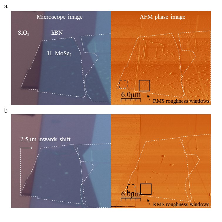 Figure 1
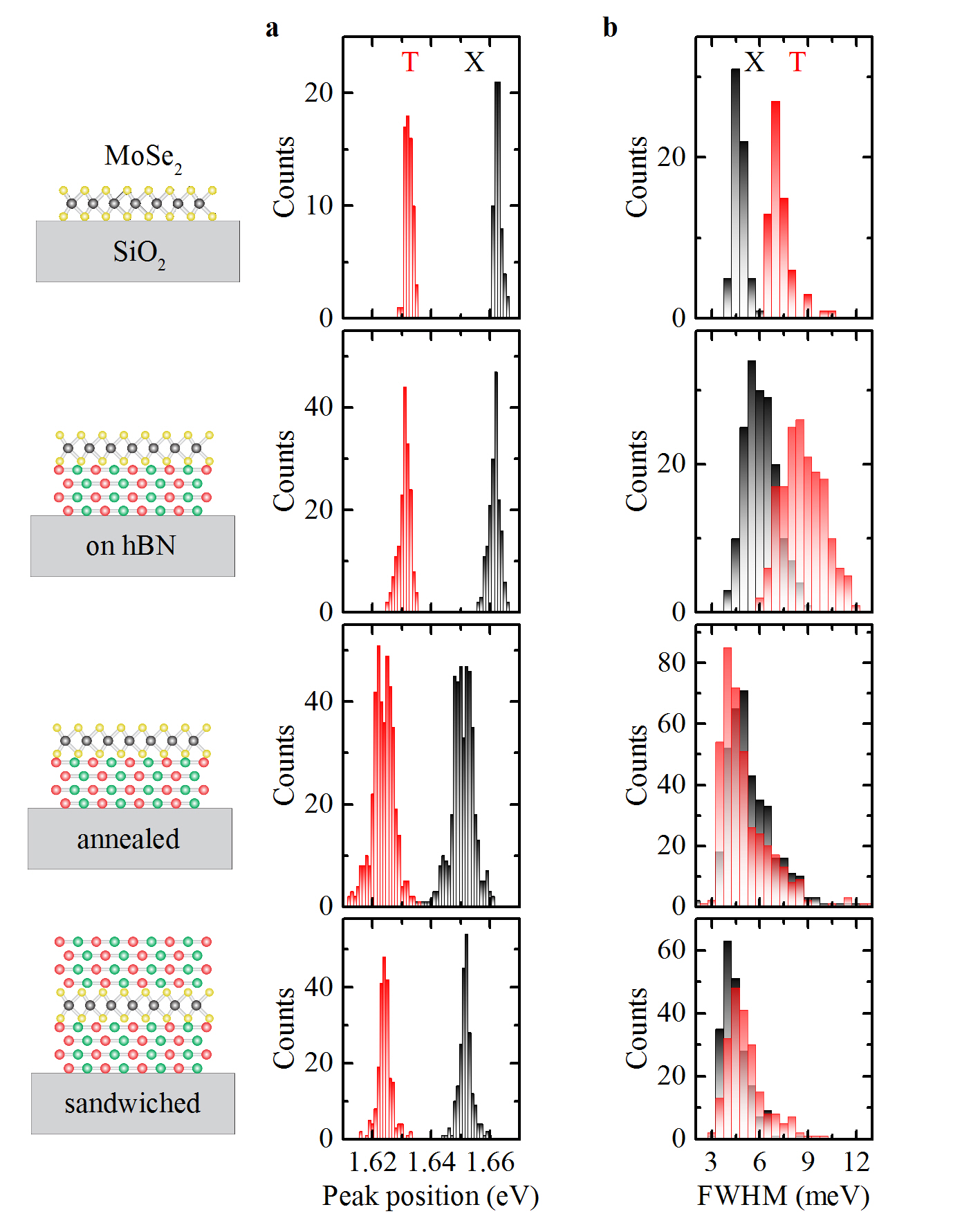 Figure 2
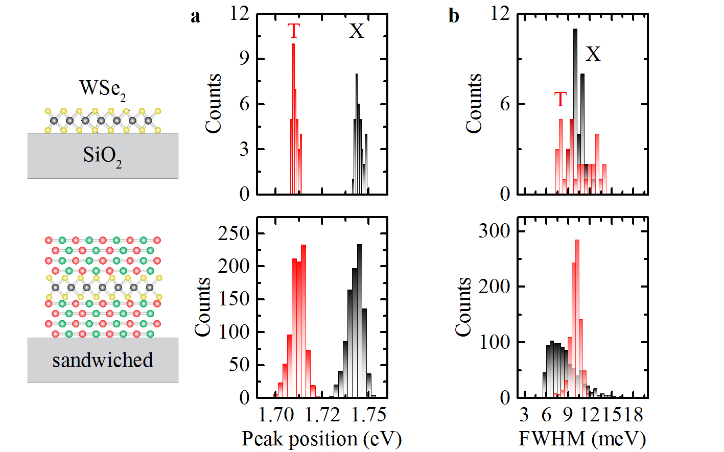 Figure 3
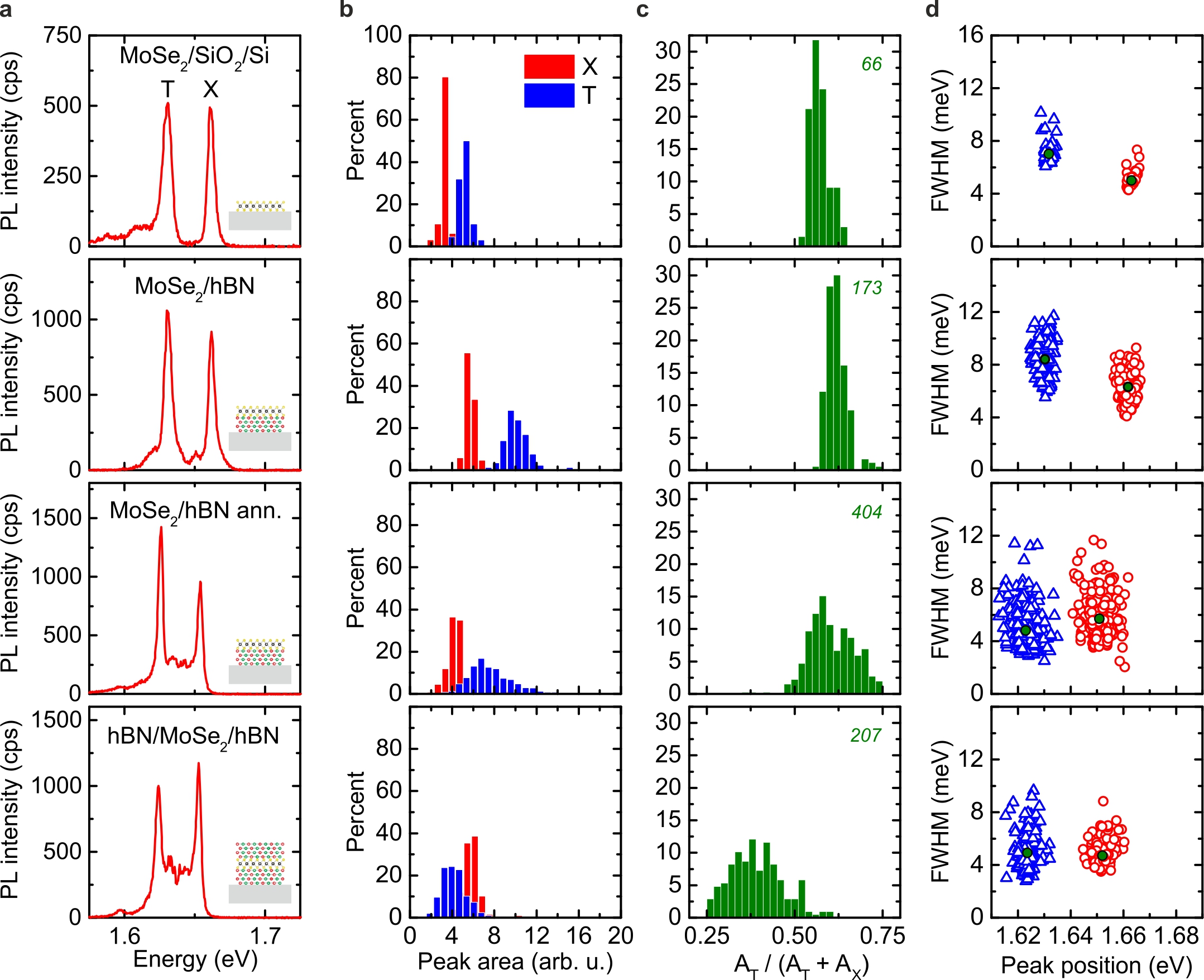 Figure 1
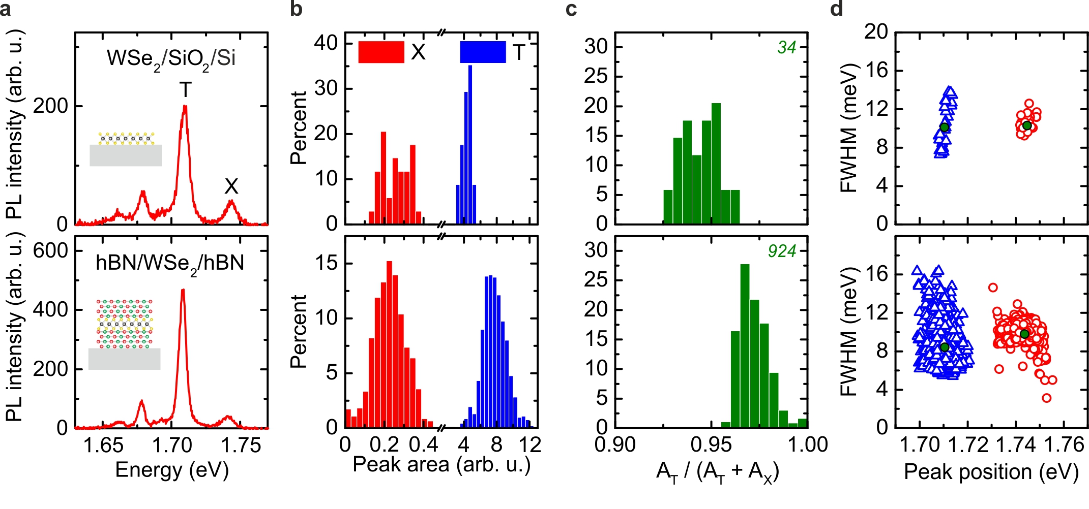 Figure 2
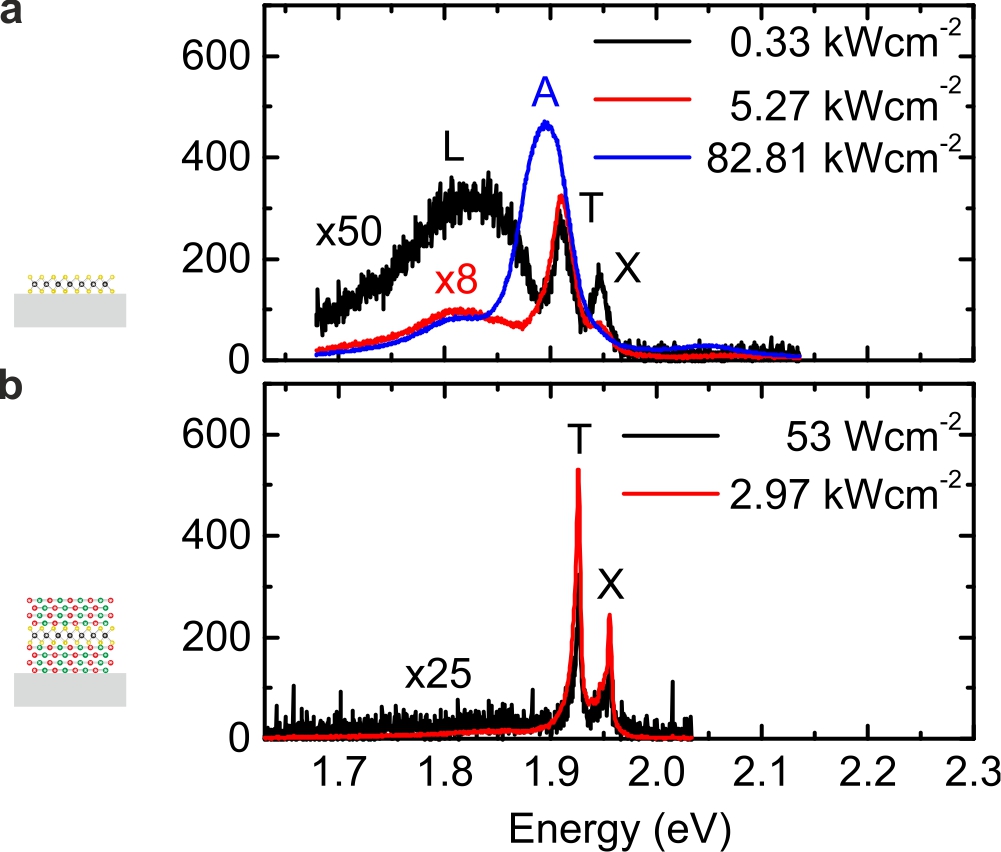 Figure 3
Peer Reviews
No public reviews on file for this paper yet. If you reviewed it on a platform where reviews are public (OpenReview, ICLR, NeurIPS, ICML), you can paste yours below so the community can read it here.
Videos
No videos yet. Explain this paper in a talk, walkthrough, or lecture? Add one.
Direct exciton emission from atomically thin transition metal dichalcogenide heterostructures near the lifetime limit
J. Wierzbowski
Walter Schottky Institut and Physik Department, Technische Universität München, Am Coulombwall 4, 85748 Garching, Germany
Nanosystems Initiative Munich (NIM), Schellingstr. 4, 80799 Munich, Germany
J. Klein
Walter Schottky Institut and Physik Department, Technische Universität München, Am Coulombwall 4, 85748 Garching, Germany
Nanosystems Initiative Munich (NIM), Schellingstr. 4, 80799 Munich, Germany
F. Sigger
Walter Schottky Institut and Physik Department, Technische Universität München, Am Coulombwall 4, 85748 Garching, Germany
C. Straubinger
Walter Schottky Institut and Physik Department, Technische Universität München, Am Coulombwall 4, 85748 Garching, Germany
M. Kremser
Walter Schottky Institut and Physik Department, Technische Universität München, Am Coulombwall 4, 85748 Garching, Germany
T. Taniguchi
National Institute for Materials Science, Tsukuba, Ibaraki 305-0044, Japan
K. Watanabe
National Institute for Materials Science, Tsukuba, Ibaraki 305-0044, Japan
U. Wurstbauer
Walter Schottky Institut and Physik Department, Technische Universität München, Am Coulombwall 4, 85748 Garching, Germany
Nanosystems Initiative Munich (NIM), Schellingstr. 4, 80799 Munich, Germany
A. W. Holleitner
Walter Schottky Institut and Physik Department, Technische Universität München, Am Coulombwall 4, 85748 Garching, Germany
Nanosystems Initiative Munich (NIM), Schellingstr. 4, 80799 Munich, Germany
M. Kaniber
Walter Schottky Institut and Physik Department, Technische Universität München, Am Coulombwall 4, 85748 Garching, Germany
Nanosystems Initiative Munich (NIM), Schellingstr. 4, 80799 Munich, Germany
K. Müller
Walter Schottky Institut and Physik Department, Technische Universität München, Am Coulombwall 4, 85748 Garching, Germany
J. J. Finley
Walter Schottky Institut and Physik Department, Technische Universität München, Am Coulombwall 4, 85748 Garching, Germany
Nanosystems Initiative Munich (NIM), Schellingstr. 4, 80799 Munich, Germany
Abstract
We demonstrate the reduction of the inhomogeneous linewidth of the free excitons in atomically thin transition metal dichalcogenides (TMDCs) MoSe2, WSe2 and MoS2 by encapsulation within few nanometer thick hBN. Encapsulation is shown to result in a significant reduction of the 10K excitonic linewidths down to 3.5\text{,}\mathrm{meV} for n-MoSe*2*, $\sim$5.0\text{\,}\mathrm{meV} for p-WSe2 and 4.8\text{,}\mathrm{meV}$$ for n-MoS2. Evidence is obtained that the hBN environment effectively lowers the Fermi level since the relative spectral weight shifts towards the neutral exciton emission in n-doped TMDCs and towards charged exciton emission in p-doped TMDCs. Moreover, we find that fully encapsulated MoS2 shows resolvable exciton and trion emission even after high power density excitation in contrast to non-encapsulated materials. Our findings suggest that encapsulation of mechanically exfoliated few-monolayer TMDCs within nanometer thick hBN dramatically enhances optical quality, producing ultra-narrow linewidths that approach the homogeneous limit.
I Introduction
In the group of atomically thin two-dimensional (2D) materials the transition metal dichalcogenides MoS2, MoSe2, WS2 and WSe2 reveal fascinating photophysical properties owing to their direct gap and strong light-matter interactionsSplendiani et al. (2010); Mak et al. (2010). The weak dielectric screening results in emission dominated by excitonic processes, with exciton binding energies on the order of several hundred He et al. (2014); Ugeda et al. (2014) that follow a non-hydrogenic Rydberg seriesChernikov et al. (2014). However, in the vast majority of reports to date the linewidths of the free excitons exhibit significant inhomogeneous broadening. This is typically attributed to the local spatial inhomogeneity of the substrate, adsorbed atoms and molecules on the surface due to the large surface-to-volume ratio and different doping and dielectric screening conditions that are highly sensitive to the choice of substrate. Broad linewidths of the exciton emission of 50\text{,}\mathrm{meV} for MoS*2*,Splendiani *et al.* ([2010](#bib.bib1)); Mak *et al.* ([2010](#bib.bib2)); Sercombe *et al.* ([2013](#bib.bib6)) $\sim$75\text{\,}\mathrm{meV} for WS2,Zhao et al. (2013) 5\text{,}\mathrm{meV} for MoSe*2* Ross *et al.* ([2013](#bib.bib8)) and $\sim$10\text{\,}\mathrm{meV} for WSe2 Zhao et al. (2013); Jones et al. (2013) have been reported in photoluminescence experiments, while time-domain spectroscopy Moody et al. (2015); Jakubczyk et al. (2016); Dey et al. (2016) and recent theory Selig et al. (2016) report homogeneously broadened luminescence linewidths in the range of 6\text{,}\mathrm{meV} depending on the material system. The healing of sulfur defects using sulfuric superacids increases the optical quantum yield and reduces the linewidths at room temperatureAmani *et al.* ([2015](#bib.bib14), [2016](#bib.bib15)); Cadiz *et al.* ([2016a](#bib.bib16)) from $\sim$70\text{\,}\mathrm{meV} to 55\text{,}\mathrm{meV}. However, low temperature studies of treated MoS*2* monolayersCadiz *et al.* ([2016a](#bib.bib16)) show that the linewidths still remain in the order of $\sim$15\text{\,}\mathrm{meV}. Very recently, it has been shown that MoS2 is particularly sensitive to photoinduced irreversible changes resulting in broad luminescence from overlapping neutral and charged exciton emissionCadiz et al. (2016b). Measurements performed using ultra-low excitation power densities reveal distinct peaks for neutral and charged excitons with linewidths of 15\text{,}\mathrm{meV}$$ for MoS2 similar to Se-based TMDCsCadiz et al. (2016b).
In this letter, we present an optical study of TMDCs encapsulated within hBN and demonstrate that encapsulation leads to a significant reduction of the linewidth observed in photoluminescence experiments, towards the radiative limit. We systematically probe modifications in the luminescence linewidth after each stacking step and extract key parameters such as the exciton peak position, relative intensities of exciton and trion recombination and peak linewidths. We also show that annealing of the heterostructure improves the spatial homogeneity of the TMDC and, thus, of the observed luminescence. From our results, we make three major observations upon hBN encapsulation: (i) the linewidths of free excitons are significantly reduced down to a few approaching the homogeneous linewidth limit, (ii) the surface is protected, preventing samples against irreversible photoinduced spectral changes and (iii) encapsulation lowers the Fermi level, reducing emission from negatively charged excitons in MoSe2, while increasing the emission from positively charged excitons in WSe2.
II Results and discussion
II.1 Sample fabrication and µ-PL measurements
The monolayer TMDCs studied in this letter are mechanically exfoliated onto degenerately n-doped Si substrates covered with a thick layer of wet-thermally grown SiO2. The heterostructures are stacked using the dry viscoelastic transfer methodCastellanos-Gomez et al. (2014), whereby we iteratively stacked hBN/TMDC/hBN onto the Si/SiO2 substrate. The hBN layer thicknesses range from to (AFM measurements). After stacking, the heterostructures were annealed at for to remove water and polymer accumulated into bubbles and improve the sample homogeneity (see supporting information).
All photoluminescence (PL) experiments were performed using a confocal microscope at . The continuous-wave excitation energy was kept at (Nd:YAG) and an excitation power density of , unless otherwise noted. The spatial mode field diameter of the focal spot ( contour) was 1.1\text{,}\mathrm{\SIUnitSymbolMicro m}$$. The detected light was filtered with a steep fluorescence filter with a transmission cut-on energy below the laser excitation energy.
II.2 Photoluminescence of encapsulated MoSe2
To probe the impact of the proximal substrate and explore the benefits of hBN encapsulation, we performed spatially resolved PL measurements and statistically analyze the emission spectra at different positions on the sample surface. Note, in our analysis we disregard spectra recorded from the edge of the flake and obviously damaged parts of the sample, as identified by conventional light microscopy. From the measurements, we extract the peak positions, full widths at half maximum linewidths (FWHM) and relative intensities of the neutral exciton (X) and charged trion (T) by fitting with Lorentzian peaks. Fig. 1 compares examples of spectra of MoSe2 on SiO2, MoSe2 on hBN, MoSe2 on hBN after annealing and MoSe2 sandwiched between hBN and after annealing. The corresponding statistical analysis of peak position, exciton linewidth and peak area for the different MoSe2/substrate configurations are shown in Fig. 1b-d, respectively. Note that in order to obtain the best comparison, in the case of MoSe2 on hBN we scan the same area after subsequent steps of stacking and annealing to trace the impact of the encapsulation on the spectral evolution. A typical spectrum recorded from MoSe2 on SiO2 is presented in Fig. 1a (top). It exhibits pronounced emission from trions, typically attributed to extrinsic effects such as doping from the substrate, mediated through trap states Mak et al. (2012); Sercombe et al. (2013); Ross et al. (2013); Jones et al. (2013) and intrinsic doping resulting from chalcogen vacancies and adsorbates that are reported to occur in mechanically exfoliated flakesKomsa et al. (2012); Hong et al. (2015). We obtain a qualitative measure of the doping by analyzing the areas of the neutral and charged exciton and and their relative spectral weight . Fig. 1b shows the peak areas, while the corresponding relative spectral weights are presented in Fig. 1c. The emission intensity for MoSe2 on SiO2 is higher for trions than for neutral excitons which is reflected by values of W > 0.5 in Fig. 1c. This remains unchanged when MoSe2 is stacked on top of 14\text{,}\mathrm{nm}$$ thick hBN, and also after annealing that only results in a slightly decreased total peak area. However, fully encapsulated MoSe2 exhibits a higher X peak-area compared to T with W < 0.5. This behaviour is indicative of a lowering of the Fermi level in the crystal inhibiting trion formation. This effect is strongest in the fully encapsulated configuration. Since the MoSe2 is exposed to ambient conditions during and after fabrication in the previous configurations, the TMDC surfaces are free to physisorption of ambient molecules Tongay et al. (2013); Miller et al. (2015), most likely H2O due to its polarity. Thus, we assume that the impact of the hBN substrate is reduced due to frozen adsorbates possibly at defects such as selenium vacancies on the TMDC surface.
Changes in the dielectric environment and doping can further influence the exciton peak positions and the linewidths (Fig. 1d)Kylänpää and Komsa (2015). Here, we directly correlate peak positions and linewidths. The exfoliated MoSe2 on SiO2 shows exciton peak positions of 1663.1\pm 1.2\text{,}\mathrm{meV} and $P_{T}=$1631.8\pm 1.3\text{\,}\mathrm{meV} with a binding energy of 31\text{,}\mathrm{meV} which is typically observed in literatureRoss *et al.* ([2013](#bib.bib8)); Wang *et al.* ([2015](#bib.bib25)). Stacking MoSe*2* on hBN results only in a slight redshift by $\Delta E\sim$-2\text{\,}\mathrm{meV} and a slightly broader distribution as can be seen in Fig. 1b. This redshift is consistent with recent calculationsKylänpää and Komsa (2015) and measurementsLin et al. (2014) considering the change in the refractive index of the substrate from n to n at the neutral exciton resonanceMalitson (1965); Gorbachev et al. (2011).
Annealing results in an additional redshift, and a total shift to a lower energy by -12\text{,}\mathrm{meV} compared to pristine MoSe*2*. This is accompanied by a much broader distribution of peak positions. The sandwiched and annealed MoSe*2* structure exhibits the strongest redshift of $\Delta E\sim$-21\text{\,}\mathrm{meV}. Yet, the statistical spread of the peak position distribution is significantly reduced from 6.8\pm 0.1\text{,}\mathrm{meV} to $s_{X}=$2.8\pm 0.1\text{\,}\mathrm{meV} (see supporting information), as depicted in the bottom panel in Fig. 1d. Moreover, the trion binding energy decreases from 31\pm 3\text{,}\mathrm{meV} to $28\pm 3\text{\,}\mathrm{meV}$ after the annealing step possibly resulting from the modification of the dielectric environment and a change in extrinsic dopingKylänpää and Komsa ([2015](#bib.bib24)). In general, we observe that the symmetric dielectric hBN environment of the MoSe*2* flake combined with annealing results in the sharpest distribution of emission energies, indicative of the highest homogeneity within the MoSe*2* flake. The statistical analysis of the linewidths for MoSe*2* on SiO*2* reveals average values of $w_{X}=$5.0\pm 0.5\text{\,}\mathrm{meV} and 7.0\pm 0.8\text{,}\mathrm{meV} for X and T excitons, respectively. Stacking MoSe*2* on hBN results in significantly higher linewidths of $w_{X}=$6.3\pm 1.0\text{\,}\mathrm{meV} and 8.4\pm 1.3\text{,}\mathrm{meV} with a much broader variation in obtained values. Annealing reduces the linewidth to $w_{X}=$5.7\pm 1.5\text{\,}\mathrm{meV} and 4.8\pm 1.5\text{,}\mathrm{meV} while capping with hBN further reduces the X linewidth to $w_{X}=$4.7\pm 0.9\text{\,}\mathrm{meV}, keeping the T linewidth at 4.9\pm 1.3\text{,}\mathrm{meV}. Interestingly, annealing reveals much higher variance of values which is significantly narrowed upon capping. However, for investigating the linewidths not only the average values are important but also the lowest values obtained. Importantly, for MoSe*2* encapsulated in hBN we observe values as low as $w_{X}\sim$3.5\text{\,}\mathrm{meV}, almost reaching the homogeneous linewidths recently reported in time-resolved four-wave-mixing experimentsJakubczyk et al. (2016); Dey et al. (2016) and theoretical calculationsSelig et al. (2016) of 2.1\text{,}\mathrm{meV}, $w_{X}\sim$3.4\text{\,}\mathrm{meV} and 5.5\text{,}\mathrm{meV}, for lattice temperatures of $T=$6\text{\,}\mathrm{K}$\text{,~{}}$5\text{\,}\mathrm{K}$\text{~{}and~{}}$10\text{\,}\mathrm{K}, respectively
With the dependence for the radiative linewidth broadeningKnorr et al. (1996); Selig et al. (2016), changing the substrate material reduces by a factor of n_{\text{SiO{}_{2}}}/n_{\text{hBN}}\approx 0.66. This then produces a radiative rate which would be quantitatively consistent with the narrowest linewidths measured in our study. Beside radiative broadening, primarily exciton-phonon coupling has been identified as broadening mechanismSelig et al. (2016). Moreover, we attribute the observed remaining broadening of the linewidth to spatial inhomogeneities of the TMDC as a result of the exfoliation procedure and residual polymer bubbles between the interfaces of the monolayer crystal and the surrounding hBN.
II.3 Photoluminescence of encapsulated WSe2
We repeated the fabrication scheme and optical experiments discussed above for MoSe2 with WSe2. Since we found the most significant improvement in optical quality for TMDCs that are fully encapsulated in hBN, we compare only the two cases of WSe2 on SiO2 and WSe2 encapsulated in hBN after annealing. Typical spectra for WSe2 on hBN are presented in Fig. 2a. The relative spectral weights are shown in Fig. 2b. Comparing the relative peak areas of the neutral and charged excitons (relative spectral weight in section II.2), results in a trend opposite to that for MoSe2. For WSe2, the relative intensity of the charged exciton increases by a factor of two upon encapsulation with hBN. We explain this trend by the difference in intrinsic doping of TMDCs present in our experiments. The MoSe2 crystal employed in this work is n-doped, which results in a negatively charged exciton. In contrast, the WSe2 is p-doped, resulting in emission from positively charged excitons (see supporting information). Thus, the hBN encapsulation effectively shifts the Fermi level in the TMDC to lower values, enabling a higher positively charged exciton formation rate.
Upon encapsulation, we observe a reduction of the neutral exciton emission linewidth from to , whilst the trion emission linewidth reduces from to . However, this effect is accompanied by a higher overall spread in the linewidth distribution for the capped material. A similar trend is observed for the distribution of peak positions. However, here only a slight redshift is observed. Notably, we observe linewidths as low as 5\text{,}\mathrm{meV} for the neutral exciton and $w_{T}\sim$5.5\text{\,}\mathrm{meV}. Recent four-wave-mixing measurementsMoody et al. (2015); Dey et al. (2016) and theoretical workSelig et al. (2016) report and predict homogeneous linewidths of 6.1\text{,}\mathrm{meV}, $w_{X}\sim$4.72\text{\,}\mathrm{meV} and 6.5\text{,}\mathrm{m}\mathrm{e}\mathrm{V}$$, respectively.
Optimised stacking processes, reducing bubble formation and wrinkling of the 2D materials could lead to desired purely lifetime broadened emission of the TMDCs.
II.4 Photoluminescence of encapsulated MoS2
In addition to the Se based TMDCs, we also applied our encapsulation scheme to MoS2 which in past experiments showed comparatively broad emission from the A-exciton Splendiani et al. (2010); Mak et al. (2010); Sercombe et al. (2013). This is attributed to inhomogeneous broadening of the emission from neutral and charged excitons that is typically so large that the two peaks are not resolved. Typical PL from MoS2 exfoliated on SiO2 is presented in Fig. 3a. For very low excitation power densities of , the spectrum (black curve) reveals emission from the neutral exciton X at , charged excitons T at and pronounced emission from the low energy L-peak is observed located 100\text{,}\mathrm{meV} below X. This broad emission is attributed to defect-related exciton emissionSplendiani *et al.* ([2010](#bib.bib1)); Mak *et al.* ([2010](#bib.bib2)); Korn *et al.* ([2011](#bib.bib30)). Upon increasing the excitation power density to $5.27\text{\,}\mathrm{kW}\text{\,}{\mathrm{cm}}^{-2}$ (red curve in Fig. [3](#S2.F3)a) the emission from the neutral exciton vanishes while charged exciton emission dominates. Meanwhile the emission from the L-peak saturates, and its contribution reduces compared to the charged exciton emission. When further increasing the excitation power density to values as high as $83\text{\,}\mathrm{kW}\text{\,}{\mathrm{cm}}^{-2}$ (blue curve in Fig. [3](#S2.F3)a), the emission merges to the broad A-exciton peak normally observed in luminescence studies of MoS*2* with a linewidth of $w_{A}\sim$53.6\pm 0.8\text{\,}\mathrm{meV}Mak et al. (2010). Note that these photoinduced changes in the form of the PL spectrum in our studies were found to be irreversible, consistent with recent findingsCadiz et al. (2016b). For the lowest excitation power densities investigated, the neutral and charged excitons exhibit linewidths of 14.7\pm 0.7\text{,}\mathrm{meV} and $w_{T}\sim$23.4\pm 0.8\text{\,}\mathrm{meV}. Here, a full statistical analysis was not possible due to the photoinduced changes in the optical spectra. In strong contrast, encapsulation of MoS2 and annealing significantly enhances the optical emission properties. The PL (Fig. 3b) exhibits bright emission from free excitons. The neutral exciton at and the trion emission at is now blue shifted by and compared to the MoS2 on SiO2 configuration, respectively. By comparing the bare monolayer on SiO2 at 5\text{,}\mathrm{kW}\text{,}{\mathrm{cm}}^{-2} to the encapsulated MoS*2* at $\sim$3\text{\,}\mathrm{kW}\text{\,}{\mathrm{cm}}^{-2} (red curves in Fig.3a and b), we observe that the relative spectral weight strongly shifts from towards lower values of . This behaviour of the relative spectral weight of the charged trion emission indicates that the hBN effectively lowers the Fermi level in the MoS2. This blueshift is accompanied by a strong decrease in X and T linewidths down to 4.8\pm 1\text{,}\mathrm{meV} and $w_{T}\sim$6.8\pm 0.9\text{\,}\mathrm{meV}, consistent with recent work by Dey *et al.*Dey et al. (2016) reporting a homogeneous linewidth of 6.6\text{,}\mathrm{meV}$$ in time-resolved four-wave-mixing measurements.
Importantly, we observe no emission from the L-peak indicative of defects and adsorbatesSplendiani et al. (2010); Mak et al. (2010); Korn et al. (2011) for the fully encapsulated sample. Such features are observed for all other sample configurations, further highlighting the importance of surface protection. Furthermore, both exciton species are well resolved and we observe no photoinduced changes even for the highest excitation power () used in our experiments.
III Conclusion
In summary, we have investigated the impact of hBN encapsulation on the optical properties of several TMDs through statistically analyzing low temperature photoluminescence experiments. Encapsulation distinctly reduces exciton linewidths and further shifts the Fermi level of the TMDCs. Moreover, surface protection especially enhances the optical quality of MoS2, resulting in very clean spectra and revealing sharp emission from neutral and charged exciton without the presence of any irreversible photoinduced changes. Our findings suggest that encapsulation of TMDCs is essential for accessing the interesting photophysical properties of MoS2 and enables more sophisticated future optoelectronic devices.
During the writing of this manuscript we recognised related work reported by Cadiz et al. Cadiz et al. (2017) and Ajayi et al. Ajayi et al. (2017).
IV Acknowledgements
We gratefully acknowledge financial support from ExQM PhD programme of the Elite Network of Bavaria, the German Excellence Initiative via the Nanosystems Initiative Munich (NIM), the Deutsche Forschungsgemeinschaft (DFG) through the TUM International Graduate School of Science and Engineering (IGSSE) and the International Max Planck Research School for Quantum Science and Technology (IMPRS-QST).
V Author contributions
J.W. and J.K. contributed equally.
VI Abbreviations
TMDC, transition metal dichalcogenides; µ-PL, Micro-photoluminescence.
VII Additional information
VII.1 Supplementary Information
Supporting information accompanies this paper.
VII.2 Competing financial interests
The authors declare no competing financial interests.
The reference list from the paper itself. Each links out to its DOI / PubMed record.
- 1Splendiani et al. (2010) A. Splendiani, L. Sun, Y. Zhang, T. Li, J. Kim, C.-Y. Chim, G. Galli, and F. Wang, Nano Letters 10 , 1271 (2010) . · doi ↗
- 2Mak et al. (2010) K. F. Mak, C. Lee, J. Hone, J. Shan, and T. F. Heinz, Physical Review Letters 105 , 136805 (2010) , ar Xiv:1004.0546 . · doi ↗
- 3He et al. (2014) K. He, N. Kumar, L. Zhao, Z. Wang, K. F. Mak, H. Zhao, and J. Shan, Physical Review Letters 113 (2014), 10.1103/physrevlett.113.026803 . · doi ↗
- 4Ugeda et al. (2014) M. M. Ugeda, A. J. Bradley, S.-F. Shi, F. H. da Jornada, Y. Zhang, D. Y. Qiu, W. Ruan, S.-K. Mo, Z. Hussain, Z.-X. Shen, F. Wang, S. G. Louie, and M. F. Crommie, Nature Materials 13 , 1091 (2014) . · doi ↗
- 5Chernikov et al. (2014) A. Chernikov, T. C. Berkelbach, H. M. Hill, A. Rigosi, Y. Li, O. B. Aslan, D. R. Reichman, M. S. Hybertsen, and T. F. Heinz, Physical Review Letters 113 (2014), 10.1103/physrevlett.113.076802 . · doi ↗
- 6Sercombe et al. (2013) D. Sercombe, S. Schwarz, O. D. Pozo-Zamudio, F. Liu, B. J. Robinson, E. A. Chekhovich, I. I. Tartakovskii, O. Kolosov, and A. I. Tartakovskii, Scientific Reports 3 (2013), 10.1038/srep 03489 . · doi ↗
- 7Zhao et al. (2013) W. Zhao, Z. Ghorannevis, L. Chu, M. Toh, C. Kloc, P.-H. Tan, and G. Eda, ACS Nano 7 , 791 (2013) . · doi ↗
- 8Ross et al. (2013) J. S. Ross, S. Wu, H. Yu, N. J. Ghimire, A. M. Jones, G. Aivazian, J. Yan, D. G. Mandrus, D. Xiao, W. Yao, and X. Xu, Nature Communications 4 , 1474 (2013) . · doi ↗