Modelling the electronic properties of GaAs polytype nanostructures: impact of strain on the conduction band character
Oliver Marquardt, Manfred Ramsteiner, Pierre Corfdir, Lutz Geelhaar,, Oliver Brandt

TL;DR
This study investigates how strain affects the electronic properties of GaAs polytype nanostructures, revealing that strain can reverse conduction band orderings and significantly influence their optical and electronic behaviors.
Contribution
The paper provides a systematic analysis of strain effects on conduction bands in GaAs polytype nanostructures, highlighting the importance of lattice mismatch and phase composition.
Findings
Strain can reverse the energy ordering of conduction bands in GaAs nanostructures.
The energy and polarization of intersubband transitions depend on phase composition.
Lattice mismatch induces intrinsic strain affecting electronic properties.
Abstract
We study the electronic properties of GaAs nanowires composed of both the zincblende and wurtzite modifications using a ten-band k.p model. In the wurtzite phase, two energetically close conduction bands are of importance for the confinement and the energy levels of the electron ground state. These bands form two intersecting potential landscapes for electrons in zincblende/wurtzite nanostructures. The energy difference between the two bands depends sensitively on strain, such that even small strains can reverse the energy ordering of the two bands. This reversal may already be induced by the non-negligible lattice mismatch between the two crystal phases in polytype GaAs nanostructures, a fact that was ignored in previous studies of these structures. We present a systematic study of the influence of intrinsic and extrinsic strain on the electron ground state for both purely zincblende…
Click any figure to enlarge with its caption.
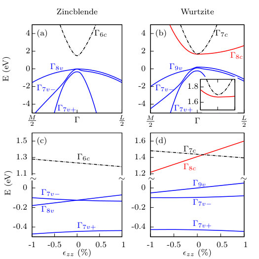 Figure 1
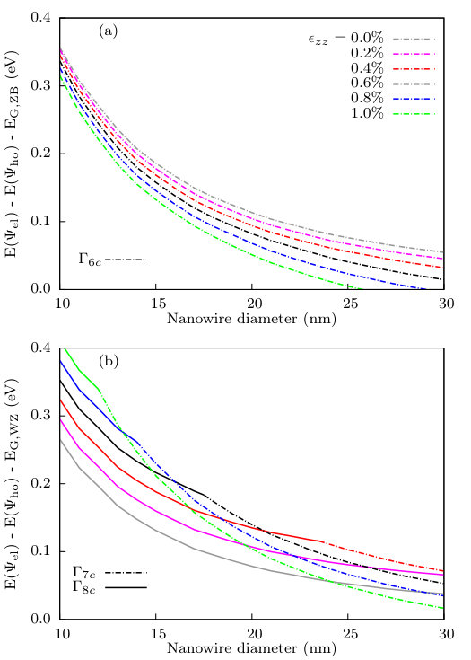 Figure 2
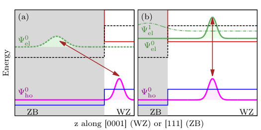 Figure 3
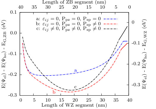 Figure 4
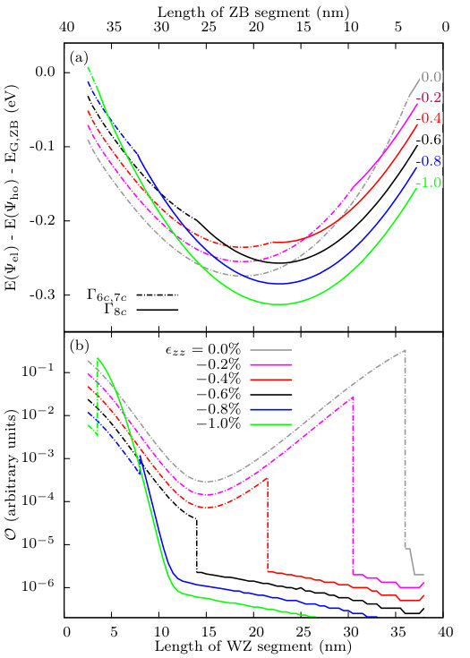 Figure 5
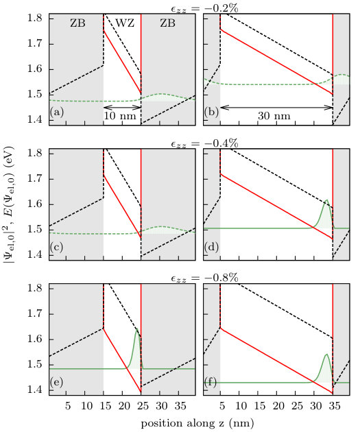 Figure 6
| Parameter | Wurtzite | Zincblende |
|---|---|---|
| (Å) | 3.955 | (3.9697) |
| (Å) | 6.526 | (6.4825) |
| (GPa) | (149.35) | |
| (GPa) | (47.52) | |
| (GPa) | (158.43) | |
| (GPa) | (50.92) | |
| (C/m2) | (0.1328) | |
| (C/m2) | () | |
| (C/m2) | 0 | |
| 13.18 | ||
| (eV) | 1.554 | 1.503 |
| (eV) | — | |
| VB offset (eV) | 0 | |
| (eV) | 0.180 | 0 |
| (eV) | 0.345 | 0.320 |
| (eV) | 28.9 | 28.0 |
| (eV) | 18.8 | 28.0 |
| () | 1.060 | — |
| () | 0.107 | — |
| () | 0.060 | 0.069 |
| () | 0.075 | 0.069 |
| 18.39 | ||
| 1.87 | ||
| 17.05 | 18.0 | |
| 6.26 | ||
| 6.83 | ||
| 7.27 | ||
| (eV) | 21.0 | 0 |
| (eV) | 5.16 | 0 |
| (eV) | ||
| (eV) | 7.68 | (8.314) |
| (eV) | 7.68 | () |
Peer Reviews
No public reviews on file for this paper yet. If you reviewed it on a platform where reviews are public (OpenReview, ICLR, NeurIPS, ICML), you can paste yours below so the community can read it here.
Videos
No videos yet. Explain this paper in a talk, walkthrough, or lecture? Add one.
Modelling the electronic properties of GaAs polytype nanostructures:
impact of strain on the conduction band character
Oliver Marquardt
Manfred Ramsteiner
Pierre Corfdir
Lutz Geelhaar
Oliver Brandt
Paul-Drude-Institut für Festkörperelektronik, Hausvogteiplatz 5–7, 10117 Berlin
Abstract
We study the electronic properties of GaAs nanowires composed of both the zincblende and wurtzite modifications using a ten-band model. In the wurtzite phase, two energetically close conduction bands are of importance for the confinement and the energy levels of the electron ground state. These bands form two intersecting potential landscapes for electrons in zincblende/wurtzite nanostructures. The energy difference between the two bands depends sensitively on strain, such that even small strains can reverse the energy ordering of the two bands. This reversal may already be induced by the non-negligible lattice mismatch between the two crystal phases in polytype GaAs nanostructures, a fact that was ignored in previous studies of these structures. We present a systematic study of the influence of intrinsic and extrinsic strain on the electron ground state for both purely zincblende and wurtzite nanowires as well as for polytype superlattices. The coexistence of the two conduction bands and their opposite strain dependence results in complex electronic and optical properties of GaAs polytype nanostructures. In particular, both the energy and the polarization of the lowest intersubband transition depends on the relative fraction of the two crystal phases in the nanowire.
I Introduction
GaAs can be considered as the prototype compound semiconductor material and is used for a wide range of electronic and optoelectronic applications including high electron mobility transistors, solar cells, and infrared laser diodes. Wa88 ; MoJa09 Consequently, the material properties of GaAs have been extensively studied and are known with higher accuracy than for any other compound semiconductor.Bl82 ; Ad94 ; VuMe01 This statement, however, only applies to the equilibrium zincblende (ZB) modification of GaAs, whereas the material properties of the metastable wurtzite (WZ) phase are poorly known.
This lack of knowledge results from the fact that WZ GaAs cannot be obtained in bulk form or by conventional heteroepitaxy.McNe05 As a consequence, there has been no need to be concerned with the properties of a metastable phase that escaped investigation in any case. However, this situation has radically changed with the advent of GaAs nanowires (NWs) in which the WZ phase is regularly observed to coexist with the ZB phase in the form of multiple ZB and WZ segments along the NW axis, i. e., or .SoCi05 ; ZaCo09 ; HeCo11 The NWs thus constitute polytype heterostructures that are interesting in their own right. However, to unambiguously extract the material properties of bulk WZ GaAs from experiments on these NWs is beset with many difficulties.
As a consequence, even fundamental properties of WZ GaAs, such as its band gap and the nature of the lowest conduction band (CB), are still controversially discussed.DePr10 ; BePa12 ; GrCo13 ; BeBe13 While the ZB phase is characterized by a single CB of symmetry with a light effective mass, two energetically close CBs exist in the WZ phase: the band, the equivalent of of the ZB phase with a comparably light effective mass, and the band, which has no equivalent in the ZB phase, but originates from folding the L valley of the ZB band structure to the center of the Brillouin zone and thus exhibits a heavy and anisotropic effective mass.TrKi99 ; BePa12 ; BeBe13 To our knowledge, all available studies agree that the energy difference between the two CBs in the WZ phase is small ( eV), but differ concerning the ordering of the two bands, namely, whether the band is energetically below the band or vice versa.DePr10 ; HeCo11 ; MuNa94 ; ChLa11 ; BePa12
The study of Cheiwchanchamnangij and LambrechtChLa11 has shown that the ordering of these two bands depends sensitively on strain. In particular, for a uniaxial strain parallel to the NW axis, the deformation potentials of the and bands were found to be of opposite signs such that the bands cross for small uniaxial strains , with the exact magnitude depending on the equilibrium lattice constants used for the calculation. This theoretical result was experimentally confirmed by Signorello et al.,SiLo14 who performed experiments on single NWs to which an external uniaxial strain was applied. Signorello et al.SiLo14 observed the / crossover at %. We note that a strain of this magnitude may also be introduced unintentionally upon dispersal of the NWs on a substrate.CoFe15
In addition to these extrinsic sources of strain, an intrinsic source exists that has so far been ignored in studies of the electronic structure of GaAs polytype NWs: the non-negligible lattice mismatch between ZB and WZ GaAs. High-resolution x-ray diffraction experiments demonstrate that the in-plane lattice constant of WZ GaAs is smaller than the equivalent interatomic distance on the (111) plane of the ZB phase by %.McNe05 ; TcHa06 ; BiBr12 ; JoYa15 Considering the sensitivity of the band structure of WZ GaAs to strain of this magnitude, it is obviously essential to take into account this lattice mismatch for the interpretation of experiments performed on polytypic GaAs NWs. As a consequence, it is imperative for any such interpretation to rely on a model that includes both the and bands in WZ GaAs explicitely.
In the present work, we employ and evaluate a ten-band model suitable to describe polytype heterostructures represented by two intersecting potentials formed by the (ZB) and (WZ) bands as well as by the (WZ) band which has no equivalent in the ZB phase. The model treats the and bands on an equal footing and thus allows us to take into account strain from both the lattice mismatch between the ZB and the WZ phase as well as from external influences. Parameters for (111)-oriented ZB systems are transformed to their respective WZ counterparts such that both crystal phases can be described within the same Hamiltonian. We compute the electronic properties of pure ZB and WZ GaAs NWs as well as of polytypic GaAs NW heterostructures. We show that strain-induced modifications of the two CBs in the WZ phase have a decisive influence on both the character and the confinement of electrons in polytype GaAs heterostructures.
II Formalism and parameters
Our simulations employ a Hamiltonian based on the eight-band model for strained WZ semiconductors developed by Chuang and Chang, ChCh96 expanded to ten bands with the parabolic band under the influence of strain. ChLa11 . This simple approach captures the fundamental feature of the potentials formed by two uncoupled, coexisting CBs in the WZ phase.
All parameters employed for the calculations are compiled in Table 1 and were taken from Ref. ChLa11, unless indicated otherwise. We have chosen the lattice constants computed within the local density approximation (LDA), since these values are much closer to the experimentally obtained lattice constantsMcNe05 ; TcHa06 ; BiBr12 than the ones obtained via the generalized gradient approximation (GGA).ChLa11 As a result, at zero strain, contrary to the ordering reported in Ref. SiLo14, in which the GGA values were used. This difference reflects the present uncertainty in parameters. In any case, the energy difference between the two bands is small, and the bands cross for uniaxial strains of the same magnitude (but opposite signs).
The notation of the deformation potentials follows the one of Ref. SiLo14, . Lattice, elastic, and piezoelectric constants of the ZB crystal along the 111 direction and the WZ phase were obtained from the respective ZB values and transformed via the relations given in Ref. ScCa11, . As there is no equivalent of the WZ band in the ZB phase, we assigned a barrier of 1.5 eV to it, which is approximately the energy separation between the and the next higher CB in the ZB phase. We have assigned the same electron effective masses as in the WZ phase for this band in the ZB segment, since the employed ten-band model requires the consistent treatment of the band in both crystal phases. The Hamiltonian (see Appendix) was implemented within the generalized multiband module of the S/PHI/nX software library. BoFr11 ; MaBo14
Figure 1 shows the bulk bandstructure as well as the response of the band edges at the point to an external uniaxial strain obtained with the parameters listed in Table 1 for both the ZB and the WZ modifications of GaAs. The familiar band structure of ZB GaAs in Fig. 1(a) is different from the band structure of WZ GaAs displayed in Fig. 1(b) not only for the valence bands (VBs), but particularly for the CBs. The energy splitting of the two CBs close to the point is visualized in the inset of Fig. 1(b).
Figures 1(c) and 1(d) illustrate the influence of an external uniaxial strain on the point CB and VB energies obtained with the parameters listed in Table 1. For the ZB phase, the VBs are degenerate at zero strain and split at any finite strain value. For the WZ phase, the VBs are split already at zero strain, and their order does not change within the intervals of strains considered here. However, the character of the lowest CB changes from to at %. This change has important consequences: not only does the energy of the optical transition change, but also the oscillator strength. BePa12
III Pure zincblende and wurtzite nanowires
We start with a discussion of the electronic properties of pure ZB and WZ NWs under the influence of strain and radial confinement. Figure 2 shows the energy difference between electron and hole ground states relative to the band gap of the corresponding phase as a function of the diameter of NWs that are subject to an uniaxial strain of up to 1%. For an unstrained ZB NW [cf. Fig. 2(a)], the energy decreases with increasing diameter due to a reduced radial confinement, and converges towards the unstrained ZB band gap. Note that dielectric confinement ZeCo16 is not considered in this model. For finite tensile strain, the energy is reduced for all diameters. The electron state has in all cases a character, as this band is energetically well separated from any other band. The hole ground state is subject to strong band mixing for all NW diameters and strains considered. The character of the hole state thus changes continuously such that no abrupt change of the hole energy is observed. The contribution of the light hole () decreases with decreasing diameter and larger strain .
The situation changes entirely when considering a pure WZ NW [Fig. 2(b)]. For the parameter set employed in the present work, the energetically lower band for the unstrained NW is the band, which exhibits a heavier effective electron mass as compared to the band. Hence, the electron ground state is of character regardless of the NW diameter. We furthermore consider the two CBs to be uncoupled, as shown for bulk WZ GaAs BeBe13 so that no band mixing occurs. Under the influence of tensile uniaxial strain, the band is lowered energetically and crosses the band for [cf. Fig. 2(d)]. For larger strains, the electron ground state is of character up to a certain diameter due to the large effective mass of this band. For larger diameters, the ground state changes its character to since the influence of quantum confinement diminishes. Since the two bands are not electronically coupled, this change of character is abrupt, in marked contrast to the behavior known from VB states in ZB GaAs NWs. Hence, WZ GaAs NWs of slightly different diameter or experiencing slightly different strain may exhibit drastically different optical properties in terms of polarization selection rules and oscillator strength. The coexistence of the and bands has thus important consequences for the interpretation of experimental results obtained from single NWs.
IV Polytype superlattices
In this section, we address the electronic properties of WZ/ZB polytype heterostructures as computed in the framework of our ten-band model. Since we are interested here in the influence of axial confinement, we restrict the following discussion to NW diameters for which radial confinement can be safely neglected, i. e., to diameters larger than 50 nm. Assuming further that other radial contributions to the potential landscape, such as surface potentials induced by Fermi level pinning, can also be excluded, we may approximate GaAs NWs consisting of WZ and ZB segments by a planar polytype heterostructure.
IV.1 Spatially direct and indirect transitions
It is generally accepted that WZ/ZB heterostructures from III-V semiconductors represent type II heterostructures with the CB minimum in the ZB phase and the VB maximum in the WZ phase.MuNa94 Consequently, electrons and holes are expected to be spatially separated in these structures. This view, however, is too simplistic in that it neglects the coexistence of two CB in the WZ phase. In fact, the and the bands form two intersecting but not interacting potentials for electrons. Figure 3 illustrates that, depending on the length of the segments, both spatially indirect and direct optical transitions are possible in a WZ/ZB heterostructure. In Fig. 3(a), the electron ground state is located in the comparatively long ZB segment due to the potential offset between the band in the ZB phase and the equivalent band in the WZ phase [cf. Tab. 1]. Since the hole ground state always resides in the WZ segment due to the / potential offset between the ZB and the WZ phase, the optical transitions are spatially indirect in this case. The situation may change for thin ZB segments as shown in Fig. 3(b). Here, the quantized state in the ZB segment is at an energy higher than the band in the WZ segment. This band has no equivalent in the ZB segment, which thus represents a high energy barrier for an electron in the WZ segment. For thin ZB segments, the electron ground state is thus confined in the potential well formed by the band in the WZ segment. Spatially direct transitions between these electrons are allowed with holes in the VB for a polarization perpendicular to the 0001 direction with a small, but nonzero dipole matrix element. The green dash-dotted line in Fig. 3 (b) indicates the first electron state that is confined in the ZB segment, which is energetically above the ground state confined in the WZ segment.
IV.2 Intrinsic strain and polarization
The above qualitative considerations show that it is essential to treat both CBs in the WZ phase on an equal footing. For quantitative results, it is important to note that the electronic properties of ZB and WZ segments in GaAs NWs are modified by strain as well as spontaneous and piezoelectric polarization potentials, and , respectively. The in-plane lattice constants of WZ and -oriented ZB crystals differ by about 0.3%. Polytype NWs will adopt an average lattice constant that depends on the overall fraction of ZB and WZ segments. These segments are thus under compressive and tensile biaxial strain with , respectively, which in turn induce a corresponding piezoelectric polarization. In addition, WZ GaAs exhibits a spontaneous polarization of C/m2 along the 0001 direction. ClSe16 The total polarization discontinuity at the ZB/WZ interfaces gives rise to a polarization potential in polytype NWs composed of ZB and WZ segments. For the following calculations, we consider a superlattice consisting of a ZB and a WZ segment with a total length of 40 nm, and individual lengths between 1 and 39 nm.
We first evaluate the influence of internal strain and built-in electric fields on the electronic properties of this WZ/ZB superlattice in the absence of additional external strain. Figure 4 shows the energy difference between electron and hole ground states relative to the band gaps of unstrained ZB and WZ GaAs as a function of the length of the WZ segment. The intrinsic biaxial strain within the segments was computed assuming that the equilibrium in-plane lattice constant is given by an average of the ZB and WZ lattice constants weighted by the respective segment length. Va89 If both the lattice mismatch and the polarization potentials are neglected [cf. curve a in Fig. 4], the energy difference between the electron and the hole ground states first drops abruptly due to decreasing hole confinement in the WZ segment, reaches a minimum at a length of 7 nm, and increases for longer WZ segments due to the increasing electron confinement in the ZB segment. The electron remains confined in the ZB segment with a character (dash-dotted line) up to a WZ segment length of 36 nm. For even longer segments, the electron ground state becomes confined in the WZ segment and its character changes to (solid line). For all segment lengths, the energy difference between electron and hole with respect to the ZB band gap remains negative, i. e., the energy of optical transitions would be below the ZB band gap due to the VB offset between ZB and WZ GaAs.
When we include spontaneous polarization in our simulations, as shown in curve b in Fig. 4, the overall energy redshifts becomes larger with increasing length of the WZ segment. At the minimum of the curve at a length of 20 nm, the energy shift amounts to 90 meV as compared to curve a. Considering, in addition, the lattice mismatch and the resulting biaxial strain and piezoelectric polarization potentials [cf. curve c], significant differences are observed with respect to curve b both for short and long WZ segments. In particular, for WZ segments longer than 36 nm, the energy difference between the electron and the hole states exceeds the band gap of ZB GaAs. Note, however, that we never reach or even exceed the band gap of WZ GaAs, which is a consequence of the presence of internal electrostatic fields in the heterostructure.
IV.3 Influence of external strain
We next study the influence of an additional uniaxial strain on the electronic properties of WZ/ZB GaAs superlattices. We focus here on the case of a superlattice with , for which the interplay of spatially direct and indirect transitions (cf. Fig. 3) is most clearly seen. Figure 5(a) shows the energy difference between electron and hole ground states as a function of the length of the WZ (ZB) segment for different values of . The intrinsic biaxial strain due to the lattice mismatch as well as spontaneous and piezoelectric polarization are taken into account. Upon the application of the external uniaxial strain, the character of the electron ground state changes to already for shorter WZ segments (for example, 30 nm at , 15 nm at , 5 nm at ), as compared to the previously discussed case where the external strain was absent (cf. Fig. 4).
This change of character can also be seen when examining the charge carrier overlap between the electron and hole ground state as defined in Ref. MaHa13, . The overlap is below between electrons and hole states for WZ segments longer than 10 nm despite the fact that both particles are confined within the same segment implying spatially direct transitions as schematically depicted in Fig. 3. The origin of this unexpected behavior is the polarization potential, which results in a strong confiment of electrons and holes at the opposite facets of the WZ segment. In contrast, the overlap between electrons confined in the ZB segment and holes in the WZ segment is much larger ( to ) thanks to the weak confinement of the light electrons. However, for and short WZ segments, increases drastically for electrons. In these cases, strain reduces the CB energy to such an amount that the electron remains confined in the WZ segment even for very short segments.
To illustrate this behavior, Fig. 6 shows the charge density of the electron ground state together with the potentials formed by the and the bands for WZ segments of 10 nm [cf. Figs. 6(a), (c), (e)] and 30 nm [cf. Figs. 6(b), (d), (f)] length and different values of . For , is confined in the ZB segment for both cases [cf. Figs. 6(a) and 6(b)], but the wavefunction penetrates into the WZ segment and the confinement of the electron is rather weak. For a strain of , the electron remains weakly confined in the ZB segment for a WZ length of 10 nm, but is transfered to the WZ segment and thus changes its character to for a WZ length of 30 nm [cf. Figs. 6(c) and 6(d)]. Evidently, the confinement of the electron in the WZ segment is much stronger due to the large effective mass of the band along the 0001 direction, so that tunneling into the ZB segment is negligible. Finally, for a strain of , the electron is strongly confined within the WZ segment for both the short and long WZ segment [cf. Figs. 6(e) and 6(f)].
V Summary and conclusions
Our findings show that the description of the electronic properties of GaAs polytype nanostructures requires the explicit consideration of the two energetically lowest CBs. We find that the intrinsic strain that arises from the lattice mismatch between the two polytypes as well as the piezoelectric and spontaneous polarization have a significant influence on the electronic properties of WZ/ZB GaAs heterostructures and must not be neglected. In particular, both the character of the electron ground state and its energy depend sensitively on the polytype fraction in a given NW. These properties are furthermore affected by external, uniaxial strain acting on the NW. For a range of , the energy difference between the two relevant CBs of the WZ phase varies between and meV. The significant influence of comparatively small strains on the optical properties of polytype GaAs NWs is a possible explanation for the controversial experimental results regarding the character of the lowest CB and the energy of the corresponding band gap that were reported in the past. We finally note that many of the parameters employed for our simulations are not known with high accuracy. However, as long as the energy difference between the and the CB of the WZ segment is small (as is the case not only in GaAs, but also in GaSb BePa12 ), the character of the electron ground state will depend on strain state and dimensions of the WZ/ZB heterostructure such that the explicit treatment of the two CBs is required for any simulation of its electronic properties.
Acknowledgements.
The authors thank Friedhelm Bechstedt for his help and valuable suggestions and Lutz Schrottke for a critical reading of the manuscript. P. C. acknowledges funding from the Fonds National Suisse de la Recherche Scientifique through project 161032.
Appendix
The Hamiltonian employed is based on an eight band model by Chuang and Chang, ChCh96 where the additional CB is added:
[TABLE]
The entities within the matrices are the operators:
[TABLE]
[TABLE]
with
[TABLE]
[TABLE]
[TABLE]
and denote the conduction and valence band edge, is the band gap, and is the bare electron mass. and are the electron effective masses of the (ZB) and (WZ) CB, and denote the crystal field and the spin-orbit splitting parameter, respectively. to are the Luttinger-like parameters. The band is added via the term:
[TABLE]
Here, denotes the energy splitting between the two bands at the -point and and denote the effective mass along the [0001] direction or perpendicular to it. denotes the small, but dipole-allowed coupling of the CB and the VB. Strain enters the Hamiltonian via the additional contribution:
[TABLE]
where:
[TABLE]
The reference list from the paper itself. Each links out to its DOI / PubMed record.
- 1(1) O. Wada, Opt. Quant. Electron. 20 , 441 (1988).
- 2(2) S. Mokkapati and C. Jagadish, Mater. Today 12 , 22 (2009).
- 3(3) J. S. Blakemore, J. Appl. Phys. 53 , R 123 (1982).
- 4(4) S. Adachi, Ga As and related materials: Bulk semiconducting and superlattice properties (World Scientific, Singapore, 1994).
- 5(5) I. Vurgaftman, J. R. Meyer, and L. R. Ram-Mohan, J. Appl. Phys. 89 , 5815 (2001).
- 6(6) M. I. Mc Mahon and R. J. Nelmes, Phys. Rev. Lett. 95 , 215505 (2005).
- 7(7) I. P. Soshnikov, G. É. Cirlin, A. A. Tonkikh, Yu. B. Samsonenko, V. G. Dubrovskii, V. M. Ustinov, O. M. Gorbenko, D. Litvinov, and D. Gerthsen, Phys. Solid State 47 , 2213 (2005).
- 8(8) I. Zardo, S. Conesa-Boj, F. Peiro, J. R. Morante, J. Arbiol, E. Uccelli, G. Abstreiter, and A. Fontcuberta i Morral, Phys. Rev. B 80 , 245324 (2009).